Effect of polycrystalline-silicon gate types on the opposite flatband voltage shift in n -type and p -type metal–oxide–semiconductor field-effect
transistors for high- k -HfO 2 dielectric
C. W. Yang, Y. K. Fang,
a)C. H. Chen, S. F. Chen, C. Y. Lin, and C. S. Lin VLSI Technology Laboratory, Institute of Microelectronics, Department of Electrical Engineering, National Cheng Kung University, Tainan, Taiwan, Republic of China
M. F. Wang, Y. M. Lin, T. H. Hou, C. H. Chen, L. G. Yao, S. C. Chen, and M. S. Liang Taiwan Semiconductor Manufacturing Co. Ltd., Hsinchu, Taiwan, Republic of China
共Received 22 October 2002; accepted 29 May 2003兲
Hafnium dioxide (HfO
2) gate dielectrics formed by the atomic layer deposition 共ALD兲 process were fabricated to investigate the flatband voltage shift ( ⌬VFB) relative to SiO
2. It is found that the direction of ⌬VFBdepends on the Fermi level position in the gate material, which shows respective positive and negative shifts in n-type and p-type metal–oxide–semiconductor field-effect transistors 共MOSFETs兲, regardless of the substrate type. The opposite direction in the flatband voltage shift is attributed to both acceptor- and donor-like interface states existing at the interface between the polycrystalline-silicon 共poly-Si兲 gate and HfO2dielectric. A model is proposed to explain the effects of poly-Si gate type on the flatband voltage shift in MOSFETs. © 2003 American Institute of Physics. 关DOI: 10.1063/1.1592634兴
depends on the Fermi level position in the gate material, which shows respective positive and negative shifts in n-type and p-type metal–oxide–semiconductor field-effect transistors 共MOSFETs兲, regardless of the substrate type. The opposite direction in the flatband voltage shift is attributed to both acceptor- and donor-like interface states existing at the interface between the polycrystalline-silicon 共poly-Si兲 gate and HfO2dielectric. A model is proposed to explain the effects of poly-Si gate type on the flatband voltage shift in MOSFETs. © 2003 American Institute of Physics. 关DOI: 10.1063/1.1592634兴
The exponential increase in the gate leakage current with decreasing oxide thickness poses a major limitation for the usefulness of conventional SiO
2.
1In order to reduce the gate tunneling current while simultaneously maintaining the same gate capacitance, high-k gate dielectrics become one of the solutions for advanced complementary metal–oxide–
semiconductor 共CMOS兲 applications.
Among the high-k dielectrics, hafnium dioxide (HfO
2) appears promising due to its relatively high dielectric con- stant ( ⬃25), wide band gap (⬃5.8 eV), and calculated ther- modynamically stability in contact with Si.
2Moreover, the integration of HfO
2into sub-100 nm device has been re- ported recently.
3,4However, device parameter issues such as the threshold voltage shift and mobility degradation remain unsolved. This is important because a high threshold voltage will prevent a device from meeting the criteria for the sub- 100 nm technology node. Therefore, the cause of the flatband voltage (V
FB) shift for HfO
2high-k dielectrics must be un- derstood.
Previous studies
5using nitride gate dielectrics found that the V
FBhas a tendency to shift negatively due to the fixed positive charge and that this phenomenon is enhanced in p-type metal–oxide–semiconductor field-effect transistors ( pMOSFETs). On the contrary, studies on Al
2O
3gate dielectrics
6found a positive V
FBshift, which can be ex- plained by the creation of fixed negative charges, and is en- hanced in n-type MOSFETs (nMOSFETs). In this work, HfO
2was found to exhibit a positive ⌬VFBfor nMOSFETs and a negative ⌬VFBfor pMOSFETs, respectively. The ori- gin of this polycrystalline-silicon 共poly-Si兲 gate type depen- dency is attribute to both donor- and acceptor-like interface states at the poly-Si and HfO
2 interface.
for pMOSFETs, respectively. The ori- gin of this polycrystalline-silicon 共poly-Si兲 gate type depen- dency is attribute to both donor- and acceptor-like interface states at the poly-Si and HfO
2interface.
pMOSFETs with a P ⫹ type gate and nMOSFETs with a
n ⫹ type gate were fabricated using a dual gate CMOS twin- well technology. After trench isolation and active area defi- nition, standard SC1/SC2 clean processes were performed on all wafers. The SC1/SC2 clean not only removes the existed native oxide fully, but also grows about a 8 Å chemi- cal oxide, which serves as a good interfacial layer between HfO
2and silicon substrate. Then, a 4-nm-thick HfO
2film was deposited by atomic layer deposition at substrate tem- perature of 300 °C using HfCl
4and H
2O as precursors. A conventional oxide of 1.8 nm was grown for comparison.
Next, a 150-nm-thick undoped poly-Si film was deposited and patterned. The n ⫹ poly-Si gate was doped with a 25 keV 1 ⫻1015 cm
⫺2 implant dose of phosphorus and the p
⫹ poly-Si gate was doped with a 10 keV 3.5⫻10
15cm
⫺2implant dose of boron. Then a spike activation anneal was done at 1050 °C. Subsequent processing steps follow a typi- cal self-aligned MOSFET process flow. A series of HfO
2capacitors with n ⫹ and p⫹ poly-Si gates on both n-well and p-well substrates were also fabricated. The equivalent oxide thickness 共EOT兲 extraction and VFB values were ex- tracted using a capacitance–voltage (C – V) simulator, which takes into account poly-Si depletion and quantum mecha- nism effects.
7
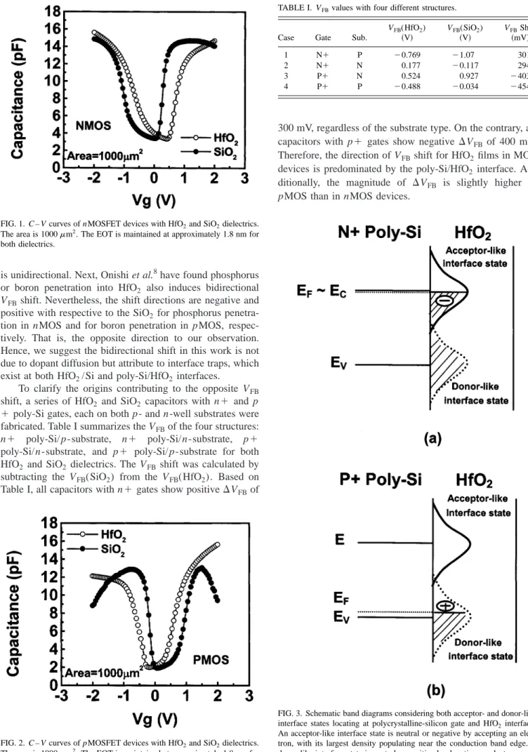
Figure 1 illustrates the C – V curves for nMOSFET de- vices with SiO
2and HfO
2gate dielectrics. Clearly, the V
FBof the HfO
2is shifted positively compared to the SiO
2. The EOT of both gate dielectrics are similar at approximately 18 Å. Figure 2 shows the C – V curves for pMOSFET devices.
In contrast, the V
FBof HfO
2shifts negatively with respect to SiO
2. The bidirectional shift is interesting. Factors leading to the V
FBshift are fixed charges, interface traps,
5and dopant diffusion.
6However, fixed charges only cause unidirectional V
FBshift, since the polarity of fixed charge is unique, i.e., positive or negative. Although Lee et al.
6reported that phos- phorus diffuses into Al
2O
3can cause V
FBshift, but the shift
a兲Electronic mail: [email protected]
APPLIED PHYSICS LETTERS VOLUME 83, NUMBER 2 14 JULY 2003
308
0003-6951/2003/83(2)/308/3/$20.00 © 2003 American Institute of Physics
Downloaded 13 Oct 2009 to 140.116.208.53. Redistribution subject to AIP license or copyright; see http://apl.aip.org/apl/copyright.jsp
is unidirectional. Next, Onishi et al.
8have found phosphorus or boron penetration into HfO
2also induces bidirectional V
FBshift. Nevertheless, the shift directions are negative and positive with respective to the SiO
2for phosphorus penetra- tion in nMOS and for boron penetration in pMOS, respec- tively. That is, the opposite direction to our observation.
Hence, we suggest the bidirectional shift in this work is not due to dopant diffusion but attribute to interface traps, which exist at both HfO
2/Si and poly-Si/HfO
2interfaces.
To clarify the origins contributing to the opposite V
FBshift, a series of HfO
2and SiO
2capacitors with n ⫹ and p
⫹ poly-Si gates, each on both p- and n-well substrates were fabricated. Table I summarizes the VFBof the four structures:
n ⫹ poly-Si/p-substrate, n⫹ poly-Si/n-substrate, p⫹
poly-Si/n-substrate, and p ⫹ poly-Si/p-substrate for both HfO
2and SiO
2dielectrics. The V
FBshift was calculated by subtracting the V
FB(SiO
2) from the V
FB(HfO
2). Based on Table I, all capacitors with n ⫹ gates show positive ⌬VFBof
300 mV, regardless of the substrate type. On the contrary, all capacitors with p ⫹ gates show negative ⌬VFB of 400 mV.
Therefore, the direction of V
FBshift for HfO
2films in MOS devices is predominated by the poly-Si/HfO
2interface. Ad- ditionally, the magnitude of ⌬VFB is slightly higher in pMOS than in nMOS devices.
FIG. 3. Schematic band diagrams considering both acceptor- and donor-like interface states locating at polycrystalline-silicon gate and HfO2 interface.
An acceptor-like interface state is neutral or negative by accepting an elec- tron, with its largest density populating near the conduction band edge. A donor-like interface state is neutral or positive by donating an electron, with its largest density populating near the valence band edge.
FIG. 1. C – V curves of nMOSFET devices with HfO2and SiO2dielectrics.
The area is 1000m2. The EOT is maintained at approximately 1.8 nm for both dielectrics.
FIG. 2. C – V curves of pMOSFET devices with HfO2and SiO2dielectrics.
The area is 1000m2. The EOT is maintained at approximately 1.8 nm for both dielectrics.
TABLE I. VFBvalues with four different structures.
Case Gate Sub.
VFB(HfO2)
共V兲
VFB(SiO2)共V兲
VFBShift共mV兲
1 N
⫹
P⫺0.769 ⫺1.07
3012 N
⫹
N 0.177⫺0.117
2943 P
⫹
N 0.524 0.927⫺403
4 P
⫹
P⫺0.488 ⫺0.034 ⫺454
309
Appl. Phys. Lett., Vol. 83, No. 2, 14 July 2003 Yanget al.
Downloaded 13 Oct 2009 to 140.116.208.53. Redistribution subject to AIP license or copyright; see http://apl.aip.org/apl/copyright.jsp
To explain the bidirectional V
FBshift, we propose the model in Fig. 3, which takes into account both donor- and acceptor-like interface states at poly-Si and dielectric inter- face. An acceptor-like interface state is neutral or negative by accepting an electron, with its largest density populating near the conduction band edge. A donor-like interface state is neu- tral or positive by donating an electron, with its largest den- sity populating near the valence band edge.
9When the poly-Si gate is n type, the Fermi level is located at the bot- tom of conduction band. The interface states with its energy level below Fermi level are filled. Therefore, the donor-like interface states are electrically neutral and acceptor-like in- terface states are electrically negative, resulting in net nega- tive charges. On the other hand, when the poly-Si is p type, the Fermi level is located near the top of valence band.
Therefore, most of the acceptor-like interface states are empty and electrically neutral. However, parts of the donor- like interface states are unfilled and electrically positive, re- sulting in net positive charges and contributing to the nega- tive V
FBshift in pMOSFETs.
As to the larger magnitude of V
FBshift in pMOSs than in nMOSs, it is probably because the depletion layer of the p-type poly-Si is more severe than the n-type poly-Si, due to the inherent nature of implanted species.
In summary, the flatband voltage shift for HfO
2films in nMOSFETs and pMOSFETs is caused by the Fermi level in the gate material, and is independent of the substrate type. A model based on the surface states at the interface of poly-Si and HfO
2is proposed. For n-type poly-Si, acceptor-like in- terface states are electrically active and lead to positive flat-
band voltage shift. Donor-like interface states are electrically active in p-type poly-Si gates, resulting in negative flatband voltage shift. Furthermore, the magnitude of flatband voltage shift is slighter larger for pMOSFETs than for nMOSFETs and is probably due to a high poly-Si depletion for the p-type poly-Si.
The authors would like to thank the members of R&D in Taiwan Semiconductor Manufacturing Co., Ltd., for wafer fabrication and technical support. The work was supported by the National Science Council under Contract Nos.
NSC91-2215-E-006-014.
1S.-H. Lo, D. A. Buchanan, and Y. Taur, IBM J. Res. Dev. 43, 327
共1999兲.
2K. J. Hubbard and D. G. Schlom, J. Mater. Res. 11, 2757
共1996兲.
3C. Hobbs, H. Tseng, K. Reid, B. Taylor, L. Dip, L. Hebert, R. Garcia, R.
Hegde, J. Grant, D. Gilmer, A. Franke, V. Dhandapani, M. Azrak, L.
Prabhu, R. Rai, S. Bagchi, J. Conner, S. Backer, F. Dumbuya, B. Nguyen, and P. Tobin, Tech. Dig. - Int. Electron Devices Meet. 2001, 651
共2001兲.
4S. J. Lee, C. H. Lee, Y. H. Kim, H. F. Luan, W. P. Bai, T. S. Jeon, and D.
L. Kwong, Solid-State and Integrated-Circuit Technology
共IEEE, Piscat-
away, NJ, 2001兲, p. 303.
5Z. Wang, C. G. Parker, D. W. Hodge, R. T. Croswell, N. Yang, V. Misra, and J. R. Hauser, IEEE Electron Device Lett. 21, 170
共2000兲.
6J. H. Lee, K. Koh, N. I. Lee, M. H. Cho, Y. K. Kim, J. S. Jeon, K. H. Cho, H. S. Shin, M. H. Kim, K. Fujihara, H. K. Kang, and J. T. Moon, Tech.
Dig. - Int. Electron Devices Meet. 2000, 645
共2000兲.
7K. Yang, Y.-C. King, and C. Hu, Technical Digest of VLSI Symposium
共IEEE, Piscataway, NJ, 1999兲, p. 77.
8K. Ohishi, L. Kang, R. Choi, E. Dharmarajan, S. Gopalan, Y. Jeon, C. S.
Kang, B. H. Lee, R. Nieh, and Jack C. Lee, Technical Digest of VLSI Symposium
共IEEE, Piscataway, NJ, 2001兲, p. 131.
9S. M. Sze, Ed., Physics of Semiconductor Devices, 2nd ed., edited by S.
M. Sze
共Wiley, New York, 1985兲, p. 380.
310 Appl. Phys. Lett., Vol. 83, No. 2, 14 July 2003 Yanget al.
Downloaded 13 Oct 2009 to 140.116.208.53. Redistribution subject to AIP license or copyright; see http://apl.aip.org/apl/copyright.jsp