Structural and dielectric characterization of the „ Ba 1 Àx Sr x …„ Ti 0.9 Sn 0.1 … O 3 thin films deposited on Pt Õ Ti Õ SiO 2 Õ Si substrate by radio frequency
magnetron sputtering
Moo-Chin Wang
a)Department of Mechanical Engineering, National Kaohsiung University of Applied Sciences, 415 Chien-Kung Road, Kaohsiung 80782, Taiwan
Cheng-Chi Tsai and Nan-Chung Wu
Department of Materials Science and Engineering, National Cheng Kung University, 1 Ta-Hsueh Road, Tainan 70101, Taiwan
Kun-Ming Hung
Department of Chemical Engineering, National Kaohsiung University of Applied Sciences, 415 Chien-Kung Road, Kaohsiung 80782, Taiwan
共Received 28 January 2002; accepted for publication 16 May 2002兲
(Ba
1⫺xSr
x)(Ti
0.9Sn
0.1)O
3(BS
xTS) thin films prepared by rf magnetron sputtering have been characterized as a function of temperature, applied voltage, and electric field. The BS
xTS thin films have been confirmed with x-ray diffraction and electron diffraction analysis. The BS
xTS thin films show a strong 共111兲 preferred orientation for Sr content 0.1⬉x⬉0.3. Grain size increases with increasing deposition temperature and is correlated to high dielectric constants. Leakage current density at 1 kV/cm varies from below 10
⫺7to mid 10
⫺9A/cm
2for the O
2/(O
2⫹Ar) ratio varying from 5/(5 ⫹5) to 1/(1⫹9). A large and clear hysteresis shows ferroelectricity at 25 °C for all BSxTS thin films. The remnant polarization increases with increasing Sr content, which is preseemably caused by the lattice mismatch between BS
xTS thin films and Pt layers. © 2002 American Institute of Physics. 关DOI: 10.1063/1.1492002兴
I. INTRODUCTION
Recently, ferroelectric thin films have been investigated as a key material for application to dynamic random access memories 共DRAMs兲, in addition to nonvolatile random ac- cess memories or the other applications.
1A ferroelectric barium strontium titanate 关Ba1⫺xSr
xTiO
3 共BST兲兴 film is of great interest for the most promising capacitor material in future DRAM applications because of its low leakage current at operating voltage as well as high dielectric constant.
2,3In the past several years, much research has been carried out focusing on deposition techniques and electrical properties of the BST films.
1,2,4 –7From a material viewpoint, BST can be categorized as a solid solution between BaTiO
3共BT兲 and SrTiO
3共ST兲 and expressed as xBT ⫺(1⫺x)ST. BT is a ferroelectric material with a Curie temperature of 120 °C, while ST is a paraelectric material with no ferroelectric phase transi- tion. Although the deposition of BST films and their dielec- trical properties have been reported,1,2,4 –7 those of the (Ba
1⫺xSr
x)(Ti
0.9Sn
0.1)O
3 共called BS
xTS hereafter 兲 thin films deposited on Pt/Ti/SiO
2/Si substrate by radio frequency 共rf兲 magnetron sputtering have not yet been studied in detail.
In the present study, the structure and dielectric proper- ties of the BS
xTS thin films deposited on Pt/Ti/SiO
2/Si sub- strates by rf magnetron sputtering have been investigated,
using x-ray diffraction 共XRD兲, scanning electron microscopy 共SEM兲, energy dispersive spectrometry 共EDS兲, scanning transmission electron microscopy 共STEM兲, electron diffrac- tion, capacitance–voltage, and current–voltage measure- ments. The preparation technique, crystallographic analysis, as well as dielectrical properties of the BS
xTS thin films have been discussed in detail.
II. EXPERIMENTAL PROCEDURE
The composition of the BS
xTS targets is listed in Table I.
Commercial BaTiO
3共Noah Tech. Co., San Antonio, TX兲, SrTiO3 共Strem Chem. Co., Newburyport, MA兲, and BaSnO
3
共Noah Tech. Co., San Antonio, TX兲 were weighed and ball milled with acetone and alumina balls for 24 h. The mixture was dried by an infrared lamp and subsequently ground and sieved. The powders through 80 mesh sieve was then mixed with 1.0 wt % of polyvinyl acetate binder and pressed at 180 MPa to form a disk of diameter 5.0 cm samples. Sintering of the samples was conducted with a heating rate of 4.5 °C/min after the binder was burned out at 600 °C for 0.5 h. The samples were then heated at a heating rate of 1.5 °C/min to 1300 °C, heating 2 h at 1300 °C, and finally cooled to room temperature at a rate of 3 °C/min.
An n-Si 共100兲 wafer was cleaned by a standard process.
The substrate has a dimension of 10 mm ⫻10 mm
⫻0.5 mm. A high quality silicon–oxide layer was grown by thermal oxidation to obtain a 200 nm thick film. The capaci- tor structure comprised Pt top and bottom electrodes with a 5 nm Ti film layer by rf magnetron sputtering from a Ti target.
a兲Author to whom correspondence should be addressed; electronic mail:
共M.-C. Wang兲
2100
0021-8979/2002/92(4)/2100/8/$19.00 © 2002 American Institute of Physics
The 500 nm Pt bottom electrode was sputter deposited at 400 °C. Both metals were sputtered in an Ar atmosphere at a pressure of 10 ⫻10⫺2Torr with an applied power of 150 W.
Next, the BS
xTS thin films with various Ba and Sr con- tents were deposited on the Pt films also by rf magnetron sputtering. The overall deposition condition for the prepara- tion of the BS
xTS thin films is listed in Table II. The Pt top electrodes with a thickness of 50 nm and diameter of 150, 250, and 350 nm were patterned by a shadow mask process.
The thickness of the BS
xTS thin films were determined with a Tencor Alpha-Step 200 profilter. The BS
xTS thin films had the composition range of x from 0 to 0.3 and the thick- ness remained around 1000 nm.
The phase identification of the BS
xTS thin films was exercised using XRD with a Cu K
␣radiation and a Ni filter, operated at 30 kV, 200 mA, and a scanning rate of 0.25°/min 共Model Rad II A, Rigaku Co., Tokyo, Japan兲. The morphol- ogy of the surface and cross section of the BS
xTS thin films were examined by SEM 共Model S-4200 field emission SEM, Hitachi, Ltd., Tokyo, Japan 兲. The composition was analyzed with EDS 共Model Noran Vantage, Boyager, USA兲 employing an internal standard method. The foils for STEM 共Model JEOL 3013, JEOL Ltd., Tokyo, Japan 兲 were prepared via the conventional technique: the samples were sliced to a thick- ness of about 30 m mechanically and ion-beam thinned to electron transparency. Selected area electron diffraction 共SAED兲 examinations were also made on carefully thinned foils of the BS
xTS thin films, operated at an accelerating voltage of 200 kV.
Dielectric constants—bias at the voltage from ⫹5 to ⫺5 V—were measured by the capacitance–voltage using a Hewlett Packard 共HP兲 4192A LF impedance analyzer. Di- electric constant-temperature curves from ⫺40 to 140 °C measured the capacitance temperature at dc voltage from ⫺5 to ⫹5 V with a stair step voltage of 0.2 V and 100 kHz, using
a HP 4263LF impedance analyzer with a mini-subzero MC-81 thermostat. Dielectric constants r were obtained from Eq. 共1兲
r⫽ cd
0A 共1兲
where c ⫽capacitance, d⫽film thickness, A⫽area of Pt top electrode, and 0⫽permitivity of empty space.
A current–voltage sweep of the Pt/BS
xTS/Pt/Ti/SiO
2/Si capacitors from 0 to 30 V was made by a HP 4156B semi- conductor parameter analyzer and dc voltage source with a stair step voltage of 0.2 V to obtain leakage current. The measurement temperature was 25 °C. A polarization-electric field ( P – E) hysteresis loop was examined using a modified Sawyer–Tower circuit with 5 kHz sine wave at 25 °C. A mica capacitor of 1 nF was used to detect the stored charge amount.
III. RESULTS AND DISCUSSION A. Structural characterization
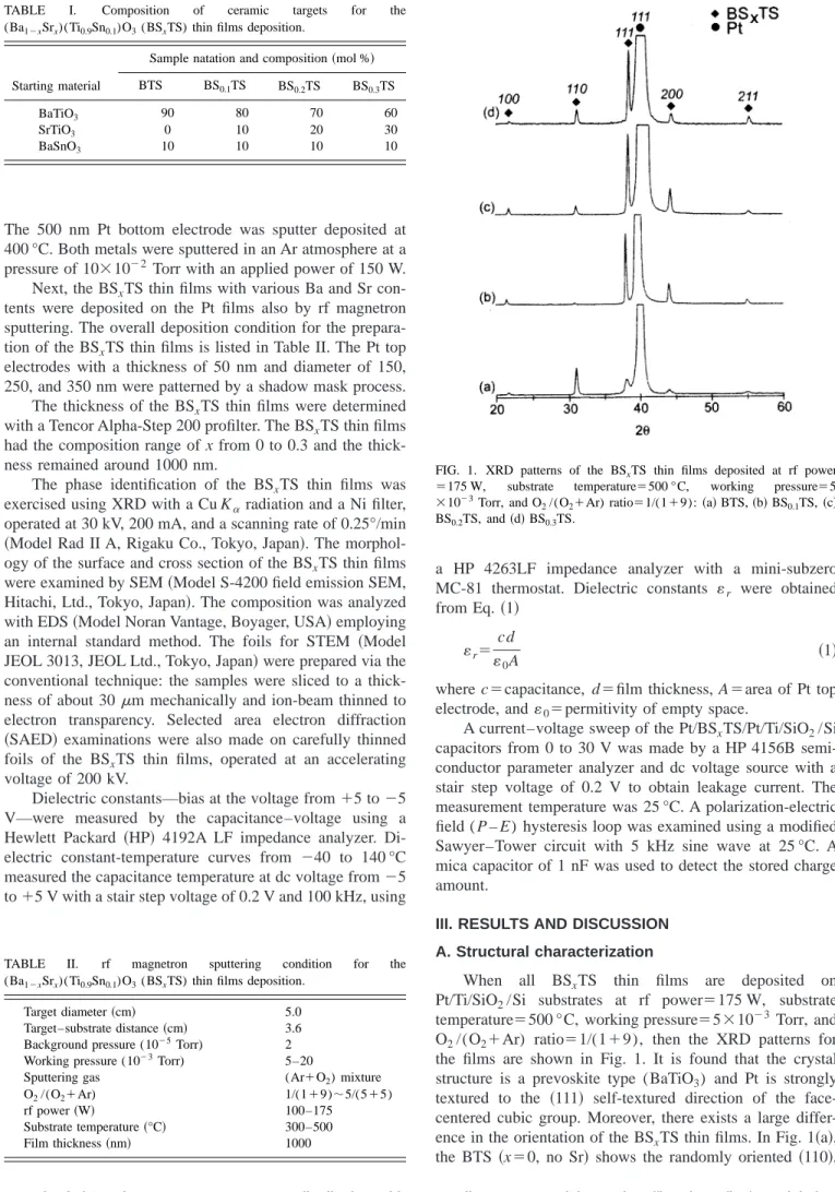
When all BS
xTS thin films are deposited on Pt/Ti/SiO
2/Si substrates at rf power ⫽175 W, substrate temperature ⫽500 °C, working pressure⫽5⫻10⫺3Torr, and O
2/(O
2⫹Ar) ratio⫽1/(1⫹9), then the XRD patterns for the films are shown in Fig. 1. It is found that the crystal structure is a prevoskite type (BaTiO
3) and Pt is strongly textured to the 共111兲 self-textured direction of the face- centered cubic group. Moreover, there exists a large differ- ence in the orientation of the BS
xTS thin films. In Fig. 1 共a兲, the BTS 共x⫽0, no Sr兲 shows the randomly oriented 共110兲,
FIG. 1. XRD patterns of the BSxTS thin films deposited at rf power
⫽175 W, substrate temperature⫽500 °C, working pressure⫽5
⫻10⫺3Torr, and O2/(O2⫹Ar) ratio⫽1/(1⫹9): 共a兲 BTS, 共b兲 BS0.1TS,共c兲 BS0.2TS, and共d兲 BS0.3TS.
TABLE I. Composition of ceramic targets for the (Ba1⫺xSrx)(Ti0.9Sn0.1)O3(BSxTS) thin films deposition.
Starting material
Sample natation and composition共mol %兲 BTS BS0.1TS BS0.2TS BS0.3TS
BaTiO3 90 80 70 60
SrTiO3 0 10 20 30
BaSnO3 10 10 10 10
TABLE II. rf magnetron sputtering condition for the (Ba1⫺xSrx)(Ti0.9Sn0.1)O3(BSxTS) thin films deposition.
Target diameter共cm兲 5.0
Target–substrate distance共cm兲 3.6 Background pressure (10⫺5Torr) 2 Working pressure (10⫺3Torr) 5–20
Sputtering gas (Ar⫹O2) mixture
O2/(O2⫹Ar) 1/(1⫹9)⬃5/(5⫹5)
rf power共W兲 100–175
Substrate temperature共°C兲 300–500
Film thickness共nm兲 1000
共111兲, 共200兲, and 共211兲 reflections. This result is similar to that of the BST films deposited on the Pt electrodes by Cha et al.8 For three other kinds, although the films are not tex- tured, the 共100兲, 共110兲, 共111兲, 共200兲, and 共211兲 reflections in these thin films are also observed and the intensity of the 共111兲 reflection is much stronger than others.
The lattice constants based on the least square refine- ment with more than 13 diffraction peaks are listed in Table III. The lattice constant of the BS
xTS thin films decreases as the molar fraction of SrTiO
3共x兲 increases. This is attributed to the smaller Sr2⫹ ionic radius 共1.44 Å兲 as compared to the Ba
2⫹ ionic radius 共1.61 Å兲. The lattice mismatch listed in Table III decreases from 3.30% to 2.70% when x 共Sr content兲 increases from 0 to 0.3.
At rf power ⫽175 W, working pressure⫽5⫻10⫺3 Torr and O
2/(O
2⫹Ar) ratio⫽1/(1⫹9), the XRD patterns of the BS
0.3TS thin films deposited on the Pt/Ti/SiO
2/Si substrate at various substrate temperatures are shown in Fig. 2. It is found that the 共111兲 reflection of the BS0.3TS thin films first appears when deposited at 300 °C 关Fig. 2共a兲兴. However, when deposited at 400 °C 关Fig. 2共b兲兴 the intensity continually increases while the 共100兲, 共110兲, 共200兲, and 共211兲 reflections
of BS
0.3TS thin films also appear. If the deposition tempera- ture is raised to 500 °C, the intensity of the 共110兲, 共111兲, and 共211兲 reflections successively increases 关Fig. 2共c兲兴. In Fig. 2, the reflections of the BS
0.3TS thin films appear when the deposition temperature is greater than 400 °C except 共111兲.
This result is in agreement with Olson et al.
9It has been pointed out that when the deposition temperature is raised to above 400 °C the BaTiO
3film becomes a crystalloid. Figure 2 also shows that although most reflections of the BS
0.3TS thin films are not distinct, the 共111兲 reflection has a strong texture. This result accordingly causes an increased atomic mobility of the thin films with increasing deposition tem- perature.
Figure 3 shows the effect of rf power on the XRD pat- terns of the BS
0.1TS thin films deposited on Pt/Ti/SiO
2/Si substrates for substrate temperature ⫽500 °C, working pressure ⫽5⫻10⫺3 Torr, and O
2/(O
2⫹Ar) ratio⫽1/(1
⫹9). It indicates that the diffraction intensity increases with increasing rf power. This result can be explained by an in- creased kinetic energy of the sputter-ejected species with in- creasing rf power.
Figure 4 shows the effect of working pressure on the XRD patterns of the BS
0.3TS thin films deposited on the Pt/Ti/SiO
2/Si substrate for rf power ⫽175 W, substrate temperature ⫽500 °C, and O2/(O
2⫹Ar) ratio⫽1/(1⫹9). It indicates that the crystallization of the BS
0.3TS thin films decreases with increasing working pressure. During sputter- ing, the target atoms or molecules are subjected to collisions with ambient gas atoms and other ejected atoms, resulting in a partial loss of energy and direction in their transit to the substrate. The motion of both sputtered atoms and ions is
FIG. 2. XRD patterns of the BS0.3TS thin films deposited at various tem- peratures, for rf power⫽175 W, working pressure⫽5⫻10⫺3Torr, and O2/(O2⫹Ar) ratio⫽1/(1⫹9): 共a兲 300 °C, 共b兲 400 °C, and 共c兲 500 °C.
FIG. 3. XRD patterns of the BS0.1TS thin films deposited at different rf powers for substrate temperature⫽500 °C, working pressure⫽5
⫻10⫺3Torr, and O2/(O2⫹Ar) ratio⫽1/(1⫹9): 共a兲 100 W, 共b兲 125 W, 共c兲 150 W, and共d兲 175 W.
TABLE III. Lattice constant of the (Ba1⫺xSrx)(Ti0.9Sn0.1)O3(BSxTS) thin films and lattice mismatch between BSxTS and Pt layer.
Sample Lattice constant共nm兲 Lattice mismatch共%兲
BTS 0.4054 ⫹3.33
BS0.1TS 0.4041 ⫹3.00
BS0.2TS 0.4037 ⫹2.90
BS0.3TS 0.4029 ⫹2.70
Pt 0.3923 —
thus impeded by the working gas atmosphere.
10At a given rf power the thermalization region shifts toward the target by increasing working pressure and results in the oxidation of the target,
11,12possible resputtering of the films,
13and/or sto- ichiometric deviation.
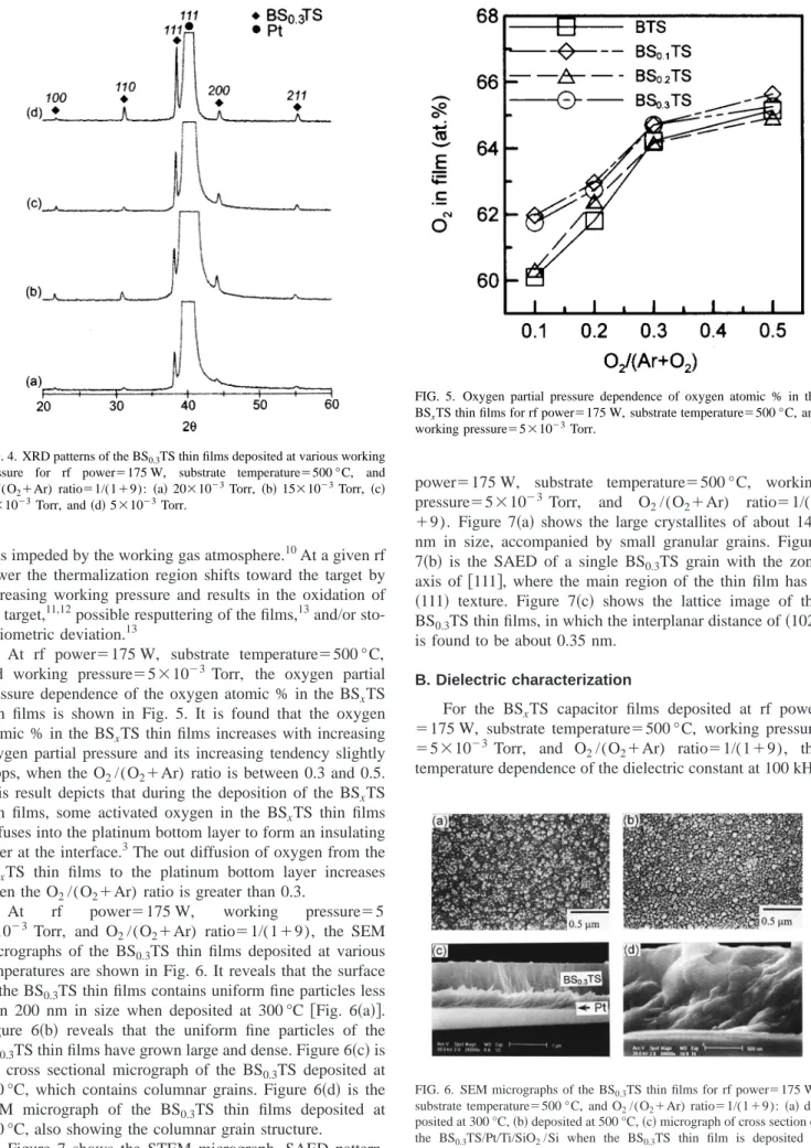
13At rf power ⫽175 W, substrate temperature⫽500 °C, and working pressure ⫽5⫻10⫺3 Torr, the oxygen partial pressure dependence of the oxygen atomic % in the BS
xTS thin films is shown in Fig. 5. It is found that the oxygen atomic % in the BS
xTS thin films increases with increasing oxygen partial pressure and its increasing tendency slightly drops, when the O
2/(O
2⫹Ar) ratio is between 0.3 and 0.5.
This result depicts that during the deposition of the BS
xTS thin films, some activated oxygen in the BS
xTS thin films diffuses into the platinum bottom layer to form an insulating layer at the interface.
3The out diffusion of oxygen from the BS
xTS thin films to the platinum bottom layer increases when the O
2/(O
2⫹Ar) ratio is greater than 0.3.
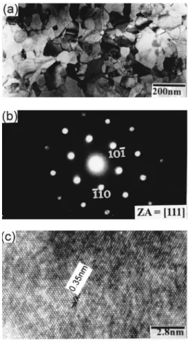
At rf power ⫽175 W, working pressure ⫽5
⫻10
⫺3Torr, and O
2/(O
2⫹Ar) ratio⫽1/(1⫹9), the SEM micrographs of the BS0.3TS thin films deposited at various temperatures are shown in Fig. 6. It reveals that the surface of the BS
0.3TS thin films contains uniform fine particles less than 200 nm in size when deposited at 300 °C 关Fig. 6共a兲兴.
Figure 6 共b兲 reveals that the uniform fine particles of the BS
0.3TS thin films have grown large and dense. Figure 6 共c兲 is the cross sectional micrograph of the BS
0.3TS deposited at 500 °C, which contains columnar grains. Figure 6 共d兲 is the SEM micrograph of the BS
0.3TS thin films deposited at 500 °C, also showing the columnar grain structure.
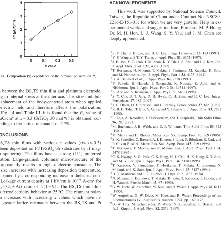
Figure 7 shows the STEM micrograph, SAED pattern, and lattice image of the BS
0.3TS thin films deposited at rf
power ⫽175 W, substrate temperature⫽500 °C, working pressure ⫽5⫻10⫺3 Torr, and O
2/(O
2⫹Ar) ratio⫽1/(1
⫹9). Figure 7共a兲 shows the large crystallites of about 140 nm in size, accompanied by small granular grains. Figure 7 共b兲 is the SAED of a single BS
0.3TS grain with the zone axis of 关111兴, where the main region of the thin film has a 共111兲 texture. Figure 7共c兲 shows the lattice image of the BS
0.3TS thin films, in which the interplanar distance of 共102兲 is found to be about 0.35 nm.
B. Dielectric characterization
For the BS
xTS capacitor films deposited at rf power
⫽175 W, substrate temperature⫽500 °C, working pressure
⫽5⫻10
⫺3Torr, and O
2/(O
2⫹Ar) ratio⫽1/(1⫹9), the temperature dependence of the dielectric constant at 100 kHz
FIG. 4. XRD patterns of the BS0.3TS thin films deposited at various working pressure for rf power⫽175 W, substrate temperature⫽500 °C, and O2/(O2⫹Ar) ratio⫽1/(1⫹9): 共a兲 20⫻10⫺3Torr, 共b兲 15⫻10⫺3Torr, 共c兲 10⫻10⫺3Torr, and共d兲 5⫻10⫺3Torr.
FIG. 5. Oxygen partial pressure dependence of oxygen atomic % in the BSxTS thin films for rf power⫽175 W, substrate temperature⫽500 °C, and working pressure⫽5⫻10⫺3Torr.
FIG. 6. SEM micrographs of the BS0.3TS thin films for rf power
⫽175 W,
substrate temperature⫽500 °C, and O
2/(O2⫹Ar) ratio⫽1/(1⫹9): 共a兲 de-
posited at 300 °C,共b兲 deposited at 500 °C, 共c兲 micrograph of cross section of
the BS0.3TS/Pt/Ti/SiO2/Si when the BS0.3TS thin film is deposited at 500 °C, showing columnar grains, and共d兲 morphology of the BS
0.3TS thin films when deposited at 500 °C.is shown in Fig. 8. It indicates that among the films with various x content the BS
xTS capacitors with x ⫽0.3 (BS
0.3TS) have the dielectric constant 225 and the BS
xTS capacitors with lower x content (x ⬍0.3) have smaller dielec- tric constants. There is a slight temperature dependence of the dielectric constant of the capacitors in the measurement temperature range between ⫺40 and 140 °C. This result is probably due to the electrical stability of the interface be- tween dielectric films and electrode layers.
On the other hand, the paraelectric to ferroelectric tran- sition is not observed for each BS
xTS thin film. BaTiO
3is a ferroelectric material with a Curie temperature of 120 °C, while SrTiO
3is a paraelectric material with no ferroelectric phase transition. In the case of Ba
0.68Sr
0.32TiO
3, thin films have a Curie temperature of around room temperature.
7In the present study, the BS
xTS thin films with various x con- tents do not show any Curie temperature in the temperature range. It is hence suggested that Sn or/and Sr addition causes the Curie temperature of the BS
xTS thin films to shift toward higher temperatures than 140 °C.
For the BS
xTS thin films deposited at rf power
⫽175 W, substrate temperature⫽500 °C, working pressure
⫽5⫻10
⫺3Torr, and O
2/(O
2⫹Ar) ratio⫽5/(5⫹5), the fre-
quency dependence of the dielectric constants measured be- tween 1 and 1000 kHz for the BS
xTS capacitors with various x contents is shown in Fig. 9. It is found that the dielectric constant decreases with increasing frequency. At lower fre- quencies, the BS
xTS capacitor has a higher dielectric con- stant, but it becomes unvaried, when the frequency is greater than 100 kHz. All curves have a sudden depression at differ- ent frequencies due to sympathetic vibration and also indi- cate a phenomenon of dielectric relaxation.
5,14,15Figure 10 shows the bias voltage dependence of the di- electric constants of the BS
xTS capacitors with various x constents. For the BS
xTS thin films sputter deposited at rf power ⫽175 W, substrate temperature⫽500 °C, working pressure ⫽5⫻10⫺3 Torr, and O
2/(O
2⫹Ar) ratio⫽5/(5
⫹5), all films have the same trend of variation and exhibit a small hysteresis. In epitaxially grown BaxSr
1⫺xTiO
3 thin films,
5a hysteresis exist with x ⭌0.44, which is not observed in the composition x ⫽0 and 0.24. Abe and Komatsu
7have pointed out that ferroelectricity is one of the explanations for the hysteresis observed in the Ba rich Ba
xSr
1⫺xTiO
3films,
FIG. 7. STEM micrograph, SAED pattern, and lattice image of the BS0.3TS thin films for rf power
⫽175 W, substrate temperature⫽500 °C, and
O2/(O2⫹Ar) ratio⫽1/(1⫹9)): 共a兲 the bright field image consists of small
granular grains,共b兲 the SAED pattern of an individual BS
0.3TS crystal with the关111兴 zone axis, and 共c兲 the lattice image shows the 共102兲 interplanar
distance of about 0.35 nm.FIG. 8. Temperature dependence of dielectric constants at 100 kHz for the BSxTS capacitors for rf power⫽175 W, substrate temperature⫽500 °C, working pressure⫽5⫻10⫺3Torr, and O2/(O2⫹Ar) ratio⫽1/(1⫹9).
FIG. 9. Frequency dependence of dielectric constants between 1 and 1000 kHz for the BSxTS capacitors for rf power⫽175 W, substrate temperature
⫽500 °C, workingpressure⫽5⫻10⫺3Torr, and O2/(O2⫹Ar) ratio⫽5/(5
⫹5).
whereas there may be some other reasons, such as ionic drift or carrier traps in dielectric films.
For the BS
0.3TS thin films deposited at rf power
⫽175 W, work pressure⫽5⫻10
⫺3Torr, and O
2/(O
2⫹Ar) ratio ⫽5/(5⫹5), the relationship between bias voltage and dielectric constant of the BS0.3TS capacitors is shown in Fig.
11. According to Figs. 11 and 10 共c兲, it indicates that the dielectric constant increases with high substrate temperature.
This result can be explained by an increase in grain size with higher deposition and growth temperatures.
5,16,17Martirena and Burfoot
18have pointed out two ways in which grain size can affect ferroelectric properties. One of them is by restrict-
FIG. 10. Relationship between bias voltage and dielectric constant of the BSxTS capacitors for rf power
⫽175 W, substrate temperature
⫽500 °C, working pressure⫽5
⫻10⫺3Torr, and O2/O2⫹Ar) ratio
⫽5/(5⫹5): 共a兲 x⫽0, 共b兲 x⫽0.1, 共c兲 x⫽0.2, and 共d兲 x⫽0.3.
FIG. 11. Relationship between bias voltage and dielectric constant of the BS0.3TS capacitors for rf power
⫽175 W, working pressure⫽5
⫻10⫺3Torr, and O2/(O2⫹Ar) ratio
⫽5/(5⫹5): 共a兲 300 °C, 共b兲 400 °C, and共c兲 500 °C.
ing the motion of domain walls which are known to contrib- ute to dielectric, piezoelectric, and elastic properties. The other is by affecting the behavior of each grain taken as a single domain.
Using Scherrers formula 关Eq. 共2兲兴, grain size has been estimated by Mikami et al.
19D ⫽ 0.9
 cos , 共2兲
where is the x-ray wavelength,  is the full width at half maximum 共FWHM兲 of the XRD peak, and is the diffrac- tion angle.
According to Fig. 2, the FWHM of the 共111兲 reflection decreases with substrate temperature increasing from 300 to 500 °C. This means the crystal size increases from 95.0 to 285 nm with substrate temperature increasing from 300 to 500 °C. It is seen in Fig. 6 共b兲, that the average grain size below 200 nm agree well with others previously reported.
5,16,17,19The relationship between leakage current density, elec- tric field of the BS
0.3TS capacitor films deposited at rf power ⫽175 W, substrate temperature⫽500 °C, and work- ing pressure ⫽5⫻10⫺3Torr is shown in Fig. 12. It is obvi- ous that the leakage current density at 1 kV/cm varies from below 10
⫺7 to mid 10
⫺9A/cm
2 for the O
2/(O
2⫹Ar) ratio varying from 5/(5 ⫹5) to 1/(1⫹9). When the O
2/(O
2
⫹Ar) ratio decreases from 5/(5⫹5) to 1/(1⫹9), the leak- age current density decreases due to increased argon influx 共i.e., decreased oxygen influx兲.
Based on the analysis of the leakage current of high- quality prycrystalline SrTiO
3thin films,
20,21the most favored mechanism is the Schottky barrier limited current flow theory. In this case, charge carriers are thermally excited over an energy barrier at the metal–ceramic interface. This barrier is created by an equilibration of the energies of charge car- riers in the metal and ceramic, and its value at zero applied field is modified by field-dependent lowering of the barrier resulting from image forces.
22When the BS
xTS thin films are deposited on the plati- num bottom electrode, some activated oxygen in the BS
xTS thin films diffuses into the bottom electrode and generates oxygen vacancies by the following equation:
O
o→V
o2⫹
⫹2e
⫺⫹
12O
2. 共3兲
Besides, the accelerated ions in the sputtering plasma may strike the surface of the BS
xTS thin films. Therefore, some activatived oxygen in the BS
xTS thin films also dif- fuses into the top electrode and generates oxygen vacancies.
These oxygen vacancies act as an electron trap site and re- duce Schottky emission barrier.
3The leakage current I
lcof the Pt/BS
xTS/Pt/Ti/SiO
2/Si capacitors can be expressed as
I
lc⫽I
se⫹I
dt⫹I
t⫹I
th, 共4兲
where I
se⫽Schottky emission current, I
dt⫽detrapping cur- rent, It⫽trapping current, and I
th⫽thermal generation cur- rent.
As mentioned above, by increasing oxygen vacancies in the BS
xTS thin films I
tincrease because of increased trap sites. On the other hand, I
sealso increases with increasing oxygen vacancies, because the Schottky emission energy barrier is reduced with increasing oxygen vacancies. Accord- ing to Fig. 5, the oxygen content in the BS
xTS thin films increases with increasing O
2/(O
2⫹Ar) ratio, and hence the oxygen vacancies are increased. Increased oxygen vacancies in the BSxTS thin films cause increased leakage current of the Pt/BS
xTS/Pt/Ti/SiO
2/Si capacitors.
Figure 13 shows the polarization versus electric field ( P – E) hysteresis curve of the BS
xTS capacitor films depos- ited at rf power ⫽175 W, substrate temperature⫽500 °C, working pressure ⫽5⫻10⫺3Torr, and O
2/(O
2⫹Ar) ratio
⫽1/(1⫹9). It is found that a large and clear hysteresis is obtained showing ferroelectricity at 25 °C.
The composition 共x兲 dependence of the remnant polar- ization P
ris shown in Fig. 14. It indicates that P
rincreases with increasing x. This result is caused by the lattice mis-
FIG. 12. Relationship between leakage current density and electric field of the BS0.3TS capacitors for rf power⫽175 W, substrate temperature
⫽500 °C, and working pressure⫽5⫻10⫺3Torr. FIG. 13. Polarization vs electric-field curves of the BSxTS capacitors for rf power
⫽175 W, substrate temperature⫽500 °C, working pressure⫽5
⫻10
⫺3Torr, and O2/(O2⫹Ar) ratio⫽1/(1⫹9).
match between the BS
xTS thin film and platinum electrode, leading to internal stress at the interface. This stress inhibits the displacement of the body-centered atom when applied with electric field and therefore affects the polarization.
From Fig. 14 and Table III, it is found that the P
rvalue of 3.35 C/cm
2at x ⫽0.3 共SrTiO3 30 mol % 兲 is obtained, cor- responding to the lattice mismatch of 2.7%.
IV. CONCLUSIONS
BS
xTS thin films with various x values (0 ⭐x⭐0.3) have been deposited on Pt/Ti/SiO
2/Si substrates by rf mag- netron sputtering. The films have a strong 共111兲 preferred orientation. Large-grained, columnar microstructure of the films apparently results in high dielectric constants. The grain size increases with increasing deposition temperature, accompanied by a corresponding increase in dielectric con- stant. Leakage current density at 1 kV/cm is 10
⫺9A/cm
2for the O
2/(O
2⫹Ar) ratio of 1/(1⫹9). The BS
xTS thin films shows ferroelectricity behavior at 25 °C. The remnant polar- ization increases with increasing x values which have in- duced greater lattice mismatch between the BS
xTS and Pt layer.
ACKNOWLEDGMENTS
This work was supported by National Science Council, Taiwan, the Republic of China under Contract No. NSC89- 2216-E-151-011 for which we are very grateful. Help in ex- perimental works and suggestion from Professor M. P. Hung;
Dr. M. H. Hon, L. J. Wang, S. Y. Yau, and J. M. Chen are deeply appreciated.
1S. Y. Cha, S. H. Lee, and H. C. Lee, Integr. Ferroelectr. 16, 183
共1997兲.
2Y. P. Wang and T. Y. Tseng, J. Appl. Phys. 81, 6762
共1997兲.
3J. H. Joo, Y. C. Jeon, J. M. Seon, K. Y. Oh, J. S. Roh, and J. J. Kim, Jpn.
J. Appl. Phys., Part 1 31, 4382
共1997兲.
4T. Horikawa, N. Mikami, T. Makita, J. Tanimura, M. Kataoka, K. Sato, and M. Nunoshita, Jpn. J. Appl. Phys., Part 1 32, 4123
共1993兲.
5B. A. Baumert et al., J. Appl. Phys. 82, 2558
共1997兲.
6Y. Fukuda, H. Haneda, I. Sakaguchi, K. Numata, K. Aoki, and A.
Nishimura, Jpn. J. Appl. Phys., Part 2 36, L1514
共1997兲.
7K. Abe and S. Komatsu, J. Appl. Phys. 77, 6461
共1995兲.
8S. Y. Cha, B. T. Jang, D. H. Hwak, C. H. Shin, and H. C. Lee, Integr.
Ferroelectr. 17, 187
共1997兲.
9J. C. Olson, D. F. Sterison, and I. Branksy, Ferroelectrics 37, 685
共1981兲.
10R. B. H. Tahar, T. Bun, Y. Ohya, and Y. Takahashi, J. Appl. Phys. 83, 2631
共1998兲.
11E. Leja, A. Kolodiez, T. Pisarkiewicz, and T. Stapinski, Thin Solid Films 76, 283
共1981兲.
12M. Buchanan, J. B. Webb, and D. F. Williams, Thin Solid Films 80, 373
共1981兲.
13M. Mehra and H. Rhodes, Mater. Res. Soc. Symp. Proc. 70, 569
共1986兲.
14S. K. Strreiffer, C. Basceri, A. I. Kingon, S. Lipa, S. Bilodeau, R. Carl, and P. C. van Buskirk, Mater. Res. Soc. Symp. Proc. 415, 219
共1996兲.
15T. Horikawa, T. Makita, and N. Mikma, Jpn. J. Appl. Phys., Part 1 34, 5478
共1995兲.
16C. S. Hwang, S. O. Park, C. S. Kang, H. J. Cho, H. K. Kang, S. T. Ahn, and M. Y. Lee, Jpn. J. Appl. Phys., Part 1 34, 5178
共1995兲.
17T. Kuroiwa, Y. Tsunemine, T. Horikawa, T. Makita, J. Tanimura, N.
Mikami, and K. Sato, Jpn. J. Appl. Phys., Part 1 33, 5187
共1994兲.
18H. T. Martirena and J. C. Burfoot, J. Phys. C 7, 3182
共1974兲.
19N. Mikami, T. Horikawa, T. Makita, K. Sato, T. Kuroiwa, T. Honda, and H. Watarai, Ferroic Mater. 43, 67
共1993兲.
20G. W. Dietz, W. Antpohler, M. Klee, and R. Waser, J. Appl. Phys. 78, 6113
共1995兲.
21W. Antpo¨hler, G. W. Dietz, M. Klee, and R. Waser, Proceedings of the Electroceramics IV., Augustinus, Aachen, 1994, pp. 169–172.
22G. W. Ditz, M. Schumacher, R. Waser, S. K. Streiffer, C. Basceri, and A. I. Kingon, J. Appl. Phys. 82, 2359
共1997兲.
FIG. 14. Composition共x兲 dependence of the remnant polarization Pr.