High quality GaN-based Schottky barrier diodes
K. H. Lee,
1S. J. Chang,
1,a兲P. C. Chang,
2Y. C. Wang,
1and C. H. Kuo
31
Institute of Microelectronics and Department of Electrical Engineering, Advanced Optoelectronic Technology Center, Center for Micro/Nano Science and Technology, National Cheng Kung University, Tainan 70101, Taiwan
2
Department of Electronic Engineering, Nan Jeon Institute of Technology, Yen-Hsui, Tainan 73746, Taiwan
3
Department of Optics and Photonics, National Central University, Jhongli, Taoyuan 32001, Taiwan
共Received 10 June 2008; accepted 14 September 2008; published online 30 September 2008兲 We report the fabrication of GaN-based Schottky barrier diodes with multi-Mg
xN
y/GaN buffer.
Compared to conventional devices with a low-temperature GaN buffer, we achieved a six orders of magnitude smaller leakage current. It was also found that effective Schottky barrier height is larger for the proposed device due to the reduction in surface defect density by using the multi-Mg
xN
y/GaN buffer. © 2008 American Institute of Physics. 关DOI: 10.1063/1.2993353 兴
In recent years, various devices have been developed using GaN-based materials grown on sapphire substrates.
1,2However, the large mismatches in lattice constant and ther- mal expansion coefficient limit the performance of these de- vices by generating a significant amount of threading dislo- cations 共TDs兲. Previously, it has been shown that one can use complex epitaxially lateral overgrowth to partially overcome this problem.
3It is also possible to reduce TD density in GaN by Si
xN
yor multi-Si
xN
y/GaN buffer due to the en- hanced lateral growth of porous Si
xN
y.
4,5Light emitting di- odes and Schottky barrier diodes 共SBDs兲 using these buffers have also been demonstrated.
6,7Very recently, Tun et al.
8reported the reduction in TD density in GaN by using multi-Mg
xN
y/GaN buffer. It was found that GaN epitaxial layer prepared on multi-Mg
xN
y/GaN buffer exhibits higher electron mobility and lower background concentration. In this letter, we report the fabrication of GaN-based SBDs with multi-Mg
xN
y/GaN buffer. Physical and electrical properties of the fabricated SBDs will also be discussed.
Samples used in this study were all grown by metal or- ganic chemical vapor deposition on sapphire substrates. The structure consists of 12 pairs of Mg
xN
y/GaN buffer and a 2.5- m-thick undoped GaN layer 共i.e., sample A兲. Samples with conventional low-temperature 共LT兲 GaN buffer were also prepared 共i.e., sample B兲. Crystal quality of the as- grown samples were evaluated by x-ray diffraction 共XRD兲 measurements. Circular SBDs were fabricated by depositing an Ohmic Ti/Al outer ring with an inner diameter of 420 m, followed by annealing. Ni/Au Schottky contact with a diameter of 400 m was deposited inside the ring opening. An HP 4156 semiconductor parameter analyzer was used to measure current-voltage 共I-V兲 characteristics of the fabricated SBDs.
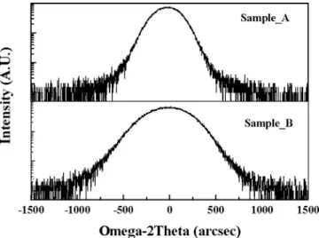
Figure 1 plots asymmetrical 共102兲 XRD rocking curves for the two samples. It was found that the full width at half maximum 共FWHM兲 of the 共102兲 XRD peaks of samples A and B were 439 and 509 arc sec, respectively. It is known that FWHM for the asymmetrical XRD rocking curve is re- lated to the overall TDs.
9The smaller asymmetrical XRD FWHM observed from sample A indicates that the crystal quality of the GaN epitaxial layer with multi-Mg
xN
y/GaN
buffer is higher. Room temperature forward I-V characteris- tics of the fabricated SBDs are shown in the inset of Fig. 2.
It was found that the turn-on voltage of sample A was slightly smaller than that of sample B. Figure 2 shows re- verse I-V characteristics measured at room temperature. With 3 V reverse bias, it was found that reverse leakage currents of samples A and B were 1.14 ⫻10
−11and 1.16 ⫻10
−5A, respectively. The significant six orders of magnitude reduc- tion in reverse leakage current observed from sample A should again be attributed to the use of multi-Mg
xN
y/GaN buffer.
Traditional method to extract ideality factor n and barrier height ⌽
Bfrom the I-V characteristic of a SBD is based on a simple thermionic emission theory. However, this approach is not valid for the diode with a series resistance R
s. In order to cater the effect of R
s, Norde 共in Ref. 10兲 proposed a method based on an auxiliary function to extract n, ⌽
B, and R
sfrom the I-V curve. Unfortunately, Norde’s method only works for ideal SBDs with n = 1. Uncertainties may also arise in determining the minimum of F共V
0, I
0兲 from the F共V兲-V plot, especially when R
sis small and the minimum cannot be determined precisely. Therefore, we adopt the method pro- posed by Cheung and Cheung
11and found that n for samples A and B were 1.28 and 2.03, respectively. Notice that n ⬎1, which suggests that there exist current transport mechanisms
a兲Electronic mail: [email protected]. FIG. 1. Asymmetrical共102兲 XRD rocking curves for the two samples.
APPLIED PHYSICS LETTERS 93, 132110共2008兲
0003-6951/2008/93共13兲/132110/3/$23.00 93, 132110-1 © 2008 American Institute of Physics
Downloaded 07 Oct 2009 to 140.116.208.56. Redistribution subject to AIP license or copyright; see http://apl.aip.org/apl/copyright.jsp
other than thermionic emission. It has been shown that trap- assisted 共dislocation related electronic states兲 tunneling dominates at T ⬍500 K while direct tunneling 共thermionic field emission 兲 dominates at higher temperature for GaN- based SBDs.
12At room temperature, the smaller ideality fac- tor for sample A should be attributed to the reduced defect density that leads to a smaller probability of trap-assisted tunneling. Using Cheung’s method,
9it was also found that
⌽
Bfor samples A and B were 1.44 and 1.04 eV, respectively.
The smaller effective ⌽
Bfor sample B should be attributed to the large defect density in the GaN films, especially sur- face pits originating from the terminations of TDs.
13To clarify the leakage current mechanism, we measured temperature dependent I-V characteristics of the samples. As shown in Figs. 3共a兲 and 3共b兲, it was found that measured reverse current densities depend on electric field and tem- perature for both samples. This suggests that leakage current is governed by the Frankel–Poole emission
14,15from a trap state within the semiconductor into a continuum of states associated with the presence of conductive dislocations. It has been shown that conduction related to threading screw dislocations in GaN is the dominant source of high leakage currents at room temperature.
16–18The current density asso- ciated with the Frenkel–Poole emission is given by
19J = ␥ E exp 冤 − q 冉 − 冑 kT qE
s
0冊 冥 , 共1兲
where E is the electric field in the semiconductor barrier at the metal/semiconductor interface, is the barrier height for electron emission from the trap state, k is Boltzmann’s con- stant, T is temperature in the unit of degrees Kelvin,
sis the relative dielectric permittivity,
0is the permittivity of free space, and ␥ is the constant. Figures 4共a兲 and 4共b兲 plots ln共J/E兲 as a function of E
1/2for samples A and B, respec- tively. It can be seen clearly that ln共J/E兲 depends linearly on E
1/2for both samples. The linear relationships indicate that leakage current is indeed dominated by the Frankel–Poole emission for both samples. We can also rewrite Eq. 共1兲 as
ln 冉 E J 冊 = A共T兲
冑E + B共T兲, 共2兲
where
A 共T兲 = 1
kT共
0
s兲
1/2q
−3/2, 共3兲
B共T兲 = ln ␥ − q
kT . 共4兲
As defined in Eqs. 共3兲 and 共4兲, we also plotted A共T兲 and B共T兲 as functions of 1 /T for both samples 共not shown兲. By ex- tracting from the plots of A 共T兲 versus 1/T, we found that
sis 5.30 and 5.41 for samples A and B, respectively. Note that the relevant dielectric constant is that at high frequency 共re- ported value of 5.35兲, rather than the static dielectric constant 共reported value of 9.5兲 共Refs 19 and 20兲 due to the electrons emitted from the trap states that do not polarize the surround- ing atoms.
18By extracting from the plots of B共T兲 versus 1/T, we found that is 0.33 and 0.23 eV for samples A and B, respectively. The larger emission barrier height observed from sample A should be attributed again to the effective suppression of TDs so that emission either into or from dislocation-related trap states will become more difficult.
FIG. 2. Reverse I-V characteristics of the fabricated SBDs. Inset shows forward I-V characteristics of the two samples.
FIG. 3. Temperature dependent I-V characteristics of 共a兲 samples A and 共b兲 B.
132110-2 Lee et al. Appl. Phys. Lett. 93, 132110共2008兲
Downloaded 07 Oct 2009 to 140.116.208.56. Redistribution subject to AIP license or copyright; see http://apl.aip.org/apl/copyright.jsp
In summary, GaN-based SBDs with conventional LT GaN buffer and with multi-Mg
xN
y/GaN buffer were both fabricated. It was found that we could significantly reduce leakage current of the SBDs by using multi-Mg
xN
y/GaN
buffer. The effective Schottky barrier height of the SBDs with multi-Mg
xN
y/GaN buffer was also found to be larger.
This work was supported in part by the Center for Fron- tier Materials and Micro/Nano Science and Technology, Na- tional Cheng Kung University, Taiwan 共Grant No. D97- 2700 兲. This work was also in part supported by the Advanced Optoelectronic Technology Center, National Cheng Kung University, under projects from the Ministry of Education.
1W. C. Lai, S. J. Chang, M. Yokoyam, J. K. Sheu, and J. F. Chen,IEEE Photon. Technol. Lett. 13, 559共2001兲.
2S. Nakamura, M. Senoh, S. i. Nagahama, N. Iwasa, T. Matsushita, and T.
Mukai,Appl. Phys. Lett. 76, 22共2000兲.
3A. Usui, H. Sunakawa, A. Sakai, and A. A. Yamaguchi, Jpn. J. Appl.
Phys., Part 2 36, L899共1997兲.
4S. Sakai, T. Wang, Y. Morishima, and Y. Naoi,J. Cryst. Growth 221, 334 共2000兲.
5S. C. Wei, Y. K. Su, S. J. Chang, S. M. Chen, and W. L. Li,IEEE Trans.
Electron Devices 52, 1104共2005兲.
6C. H. Kuo, S. J. Chang, Y. K. Su, C. K. Wang, L. W. Wu, J. K. Sheu, T. C.
Wen, W. C. Lai, J. M. Tsai, and C. C. Lin,Solid-State Electron. 47, 2019 共2003兲.
7J. D. Jhou, S. J. Chang, Y. K. Su, Y. Y. Lee, C. H. Liu, and H. C. Lee, Appl. Phys. Lett. 91, 103506共2007兲.
8C. J. Tun, C. H. Kuo, Y. K. Fu, C. W. Kuo, C. J. Pan, and G. C. Chi,Appl.
Phys. Lett. 90, 212109共2007兲.
9B. Heying, X. H. Wu, S. Keller, Y. Li, D. Kapolnek, B. P. Keller, S. P.
DenBaars, and J. S. Speck,Appl. Phys. Lett. 68, 643共1996兲.
10K. Sato and Y. Yasumura,J. Appl. Phys. 58, 3655共1985兲.
11S. K. Cheung and N. W. Cheung,Appl. Phys. Lett. 49, 85共1986兲.
12S. Karmalkar, D. M. Sathaiya, and M. S. Shur,Appl. Phys. Lett.82, 3976 共2003兲.
13J. K. Sheu, M. L. Lee, and W. C. Lai, Appl. Phys. Lett. 86, 052103 共2005兲.
14P. Kozodoy, J. P. Ibbetson, H. Marchand, P. T. Fini, S. Keller, J. S. Speck, S. P. DenBaars, and U. K. Mishra,Appl. Phys. Lett. 73, 975共1998兲.
15J. Spradlin, S. Dogan, J. Xie, R. Molnar, A. A. Baski, and H. Morkoç, Appl. Phys. Lett. 84, 4150共2004兲.
16J. E. Northrup,Appl. Phys. Lett. 78, 2288共2001兲.
17J. W. P. Hsu, M. J. Manfra, R. J. Molnar, B. Heying, and J. S. Speck,Appl.
Phys. Lett. 81, 79共2002兲
18J. R. Yeargan and H. L. Taylor,J. Appl. Phys. 39, 5600共1968兲.
19A. S. Barker Jr., and M. Ilegems,Phys. Rev. B 7, 743共1973兲.
20S. Fischer, C. Wetzel, E. E. Haller, and B. K. Meyer,Appl. Phys. Lett. 67, 1298共1995兲.
FIG. 4. Plots of ln共J/E兲 vs E1/2for共a兲 Samples A and 共b兲 B, with tempera- ture ranging from 150 to 400 K.
132110-3 Lee et al. Appl. Phys. Lett. 93, 132110共2008兲
Downloaded 07 Oct 2009 to 140.116.208.56. Redistribution subject to AIP license or copyright; see http://apl.aip.org/apl/copyright.jsp