國立臺灣大學工學院材料科學與工程學研究所 博士論文
Department of Materials Science and Engineering College of Engineering
National Taiwan University Doctoral Dissertation
電磁共振效應用於材料光外耦合增益之研究
Using Electromagnetic Resonance Effects to Develop the Techniques of Material Light-Out-Coupling
Enhancement
曾奕鈞 Yi-Chuan Tseng
指導教授:陳學禮 博士 Advisor: Hsuen-Li Chen, Ph.D.
中華民國 105 年 9 月
September, 2016
口試委員會審定書
誌謝
在充實的博士研究中,鮮少有機會於生活中仔細地檢視過去。完成這本博士 論文後,回顧才發現有太多人在幫助和支持自己。科學和工程上的研究充滿著樂 趣,但是與自然界打交道,難免孤獨。所幸一路上如此多人的幫助使我覺得這條 路途並沒那麼艱辛。能夠完成這本博士論文,最要感謝我的指導教授陳學禮博士。
在老師的指導下,帶領我進入光學的世界、引導我探索科學的方法、教誨我邏輯 上的思考以及指導我呈現研究的方式;我的收穫實在太多,著實難以使用三言兩 語道盡感謝之意。老師亦師亦友,在生活上與我分享的人生觀,亦使我面對生活 的態度與高度有所成長。
感謝口試委員王子建教授、鄭劭家教授、謝健教授、曾盛豪教授以及陳仕鴻 博士。委員們對於研究和論文的建議指導,使我的論文更加完整與豐富;透過不 同領域的見解,亦領導我從不同角度檢視自己的研究。其中,特別感謝鄭劭家老 師,除了給予我指導建議,亦大方地出借實驗室的貴重儀器,使我的論文研究可 以更容易地進行。
感謝德輝學長、紹欽學長、善仁學長、鴻森大哥,學長和前輩們在研究和實 驗中的建議以及研究生活上的經驗使我的博士研究之路更加順遂。也要感謝宇倫、
紹良兩位同學,感謝你們在路上一直相伴、互相幫忙,我們培養了絕佳的默契,
也令我大幅地降低了這條路上的孤寂感受。感謝德宸、禹萱、致宇、泰言、宜群、
程毅、冠宏、長卿、弘正、欣宜、寶勻、妤庭、廷偉、博義、恩芸、怡君、郁佳、
泰騏、博淵、庭維、忠華、隆泰、祐維、少聰、至傑、致凱、沛儒,感謝你們給 我許多研究上的協助、生活上的陪伴;與你們的相處有太多豐富精彩的回憶。感 謝耕德、子堯和思偉的諸多協助幫忙,你們對於此論文的內容,具有重要的影響 性。我特別要感謝仰淳及振傑,謝謝你們兩人的無私、利用自己在博士班忙碌研 究中的寶貴時間,給予我許多研究上的幫助及經驗。沒有你們的大力相挺,這本 博士論文絕對沒有辦法如此順利地完成。這個階段能夠結識你們兩位,我實在太
幸運了。
父母親無疑在每個人生命中扮演最重要的腳色,沒有我的父親曾光榮先生、
母親吳雯倩女士,就不會有此論文的誕生。父親在學術界的經驗歷練及對兒子無 條件奮不故身的付出,成為了我最強壯的靠山。母親雖人在國外,但是自幼的敦 敦教誨成就了我積極的人格,沒有你們就不會有今天的我。家人之中,弟弟奕瑋 亦對我相當支持,從聊天談論人生方向到教我一些專業繪圖技巧,都給我許多動 力。博士研究是目前的人生中最重要的里程碑,而家庭則完整了我整個人生。
我亦要感謝我的未婚妻許幼宜大美女(她本人堅持必須以大美女稱呼)。在 這一個艱困的階段裡,感謝這個女孩為我奉獻自己重要的青春時光,提供了經濟 和精神上的全力支持;在我每次跌倒時妳無法扶我卻陪我學忍痛。也感謝我的摯 友許芳宜,在整個攻讀博士的漫長時光中,提供我如此不具壓力的溫暖支持。
隨著誌謝辭的完成,論文的全文也算是逐漸地完成了。再次提醒自己因為有 你們大家,讓這篇論文更加完整,亦在我的博士研究階段充實了我的生活。也許 也有許多曾為我付出過的人,我並未於誌謝辭中提及,請原諒我的疏忽。最後引 用陳之藩先生「謝天」中所述,無論什麼事,不是需要先人的遺愛與遺產,即是 需要眾人的支持與合作,還要等候機會的到來。我深感自己貢獻之渺小,因為需 要感謝的人太多了。
曾奕鈞 僅緘於 國立台灣大學材料科學與工程學研究所 中華民國一百零五年九月二十五號
摘要
材料的光外耦合技術在近期相當吸引科學界的注目,尤其在於提升材料的非 線性光學現象,例如表面增益拉曼散射。相對於線性的彈性碰撞而雷利散射之光 子數目來說,非彈性碰撞而產生的拉曼散射之光子數量相當貧乏。因此提高材料 的光外耦合,可以有效地提高得以偵測到的光子數量,進而擴展拉曼檢測的應用 範疇。光外耦合技術亦被提出應用於螢光材料,透過材料的光外耦合技術,得以 大幅提升材料的發光效率。在過往的研究中,光外耦合技術多以金屬奈米結構提 升侷域電磁場強度進而達到提高發光效果為主。然而,這些金屬奈米結構都容易 對於發光材料產生摻雜、驟熄等影響;除此之外,金屬奈米結構亦有本身對於入 射光發生吸收以及其產生侷域電磁場範圍不足等缺點。高折射率的介電奈米材料 會對於特定波長的入射電磁波產生磁性共振,誘發其本身內部及向鄰近材料延伸 的高電磁場熱區。本論文之研究主要即是利用此磁性共振產生的高電磁場熱區提 高材料的光外耦合效應。
我們發現一個透過非金屬結構磁偶極共振產生大面積電磁場熱區進而提升 基板拉曼訊號的方法。透過設計高折射率之矽奈米粒子的尺寸,使得入射電磁波 在奈米粒子的內部產生磁性共振。我們發現良好分散的矽奈米粒子透過其本身磁 性共振下凝聚於粒子內部的高電磁場,得以使矽奈米粒子單位體積下的拉曼增益 達到近六萬倍。由非金屬奈米粒子產生的強電磁場熱區不僅存在於奈米粒子內部 及周圍,亦延伸至與奈米粒子接觸的下方基板內部。我們透過實驗,將覆蓋率低 於百分之零點三的矽奈米粒子佈局於氮化鎵及碳化矽基板表面;即觀察到此二基 板之拉曼散射訊號明顯的增強超過百分之五十。我們在對照的實驗之中,將具有 侷域性表面電漿共振行為的金屬奈米粒子佈局於相同的基板表面,基板的拉曼散 射訊號則無明顯的增益情形。我們觀察到相對於金屬奈米結構產生的侷域性表面 電漿共振,由非金屬奈米共振腔產生的磁偶極共振現象可以更加有效率的增加位
於共振腔下方之待測分子的拉曼散射訊號。相對於金屬奈米結構,非金屬共振腔 的磁偶極共振亦展現出較大的有效增益拉曼散射範圍。此由非金屬結構產生的磁 偶極共振具有相當良好的潛力進而發展次世代的非金屬電磁增益技術。
為了穩定地獲得石墨烯,化學氣相沉積大面積的碳原子於金屬表面已經廣泛 地被接受為一個有效的方式。因此,及時非破壞性地監測金屬基板表面的石墨烯 亦成為了重要的考量。雖然得以透過光學上的拉曼光譜進行監測,但石墨烯於金 屬表面僅能產生相當微弱的拉曼訊號。我們將具有特定尺寸、符合入射電磁波磁 偶極共振的矽奈米粒子佈局於透過化學氣相沉積的石墨烯銅箔上方,巧妙位於石 墨烯的位置引發了一個相當強烈的電磁場區域。利用模擬,我們發現此位於石墨 烯位置高達超過一百二十倍的高電磁場強度來自矽奈米粒子磁偶極共振的位移 電流與下方銅箔內部的自由載子之耦合。除了位於石墨烯之高強度的電磁場,我 們還觀察到矽奈米粒子亦有效率地在石墨烯內部產生相當大範圍的電磁場熱區。
我們在實驗上證明了透過此高強度、大範圍的電磁場熱區,銅箔上方的石墨烯之 拉曼訊號可以被大幅地增益超過兩百倍。此外,實驗上亦觀察到矽奈米粒子對於 原始石墨烯的拉曼訊號幾乎沒有影響;覆蓋於石墨烯上方的矽奈米粒子也可以輕 易地被移除。本論文同時呈現了應用此方式透過拉曼測定位於不同晶粒尺寸銅箔 基板上方之不同石墨烯的品質;驗證了此方法可以達到及時非破壞性地進行拉曼 訊號增益之應用。
由於矽塊材典型的非輻射再結合特性,其具有相當低的量子效率;相對於具 有直接能隙的材料,矽塊材被一般認定為「暗」材料。在本論文中,透過上述磁 偶極共振發生時的矽奈米粒子會於粒子內部產生強烈的電磁場,我們發現此電磁 場可以誘使九十至一百二十奈米直徑之矽奈米粒子發生聲子協助放光現象。在這 個尺寸下,矽奈米粒子不具有量子限域效應。藉由模擬,我們發現設定於矽奈米 粒子內部的點光源在放光光譜上的峰值位置符合其磁偶磁共振的發生位置。因此 我們進而設計了一個可以提升矽奈米粒子之磁偶極共振的奈米共振腔基板。透過
實驗上將矽奈米粒子放置於此基板上方,觀察到磁偶極共振波長下的矽奈米粒子 明顯地放光。估計此時矽奈米粒子的量子轉換效率達到百分之二點四。實驗上我 們亦透過降低矽奈米粒子的尺寸改變其磁偶極共振發生的波長,進而在不同波長 下觀察到矽奈米粒子的發光藍移現象。這個實驗提供了一個清楚的證據指出由磁 偶極共振產生於矽奈米粒子內部的強烈電磁場可以誘發其聲子協助放光現象。根 據我們的調查,在本論文之前尚未有文獻提出矽材料在這個尺寸下得以輻射出可 見光。因此,我們建議,磁性共振下的矽奈米材料相當具有潛力應用於開發下一 世代的「全光程矽光子學」。
關鍵字:矽奈米粒子、磁偶極共振、表面增強拉曼散射、石墨烯、矽發光
Abstract
Recently, techniques of material light-out-coupling have attracted considerable attention in the scientific community, especially, to enhance the material light-out-coupling in nonlinear optical phenomenon such as surface enhanced Raman scattering. In previous literatures, the main methods to achieve the material light-out-coupling are by employing the electromagnetic field generated from metal nanostructures. However, generally, the metal nanostructures might dope and quench the fluorescent materials. In addition, the metal nanostructures might also absorb light to reduce the emission efficiency of the fluorescent materials. Dielectric materials having high refractive index can be induced a magnetic resonance for the incident electromagnetic wave having a specific wavelength. The magnetic resonance can induce an intense electromagnetic field hot zone inside the dielectric materials. The hot zones of intense electromagnetic field can be generated not only within the dielectric materials but also around them, even within the nearby materials. The main studies in this thesis are enhancing the material light-out-coupling by using the intense electromagnetic field generated from the magnetic resonance.
We found that the large area of electromagnetic field hot zone induced through magnetic dipole resonance of metal-free structures can greatly enhance Raman scattering signals. The magnetic resonant nanocavities, based on high-refractive-index silicon nanoparticles (SiNPs), were designed to resonate at the wavelength of the excitation laser of the Raman system. The well-dispersed SiNPs that were not closely packed displayed significant magnetic dipole resonance and gave a Raman enhancement per unit volume (REV) of 59347. The hot zones of intense electric field were generated not only within the nonmetallic NPs but also around them, even
(GaN) and silicon carbide (SiC) surfaces presenting very few SiNPs (coverage:
<0.3%) could display significantly enhanced (>50%) Raman signals. These nonmetallic NPs displaying magnetic dipole resonance were more effective at enhancing the Raman scattering signals from analytes that were underlying, or even far away from, them. This application of magnetic dipole resonance in metal-free structures appears to have great potential for use in developing next-generation techniques for Raman enhancement.
Chemical vapor deposition (CVD) large-area crystal carbon atom on metal surface to stably obtain graphene is widely accepted as an effective method, thereby, in-situ and non-destructive characterizing the properties of the graphene on a metal substrate became a considerably important issue. Raman spectroscopy is very useful for identifying the properties of graphene, unfortunately, the as-grown graphene on a metal substrates provides a very weak Raman signal. In this thesis, we arrange the SiNPs having a specific dimension and an internal magnetic dipole resnance upon the CVD-as-grown graphene/Cu foil and cleverly give rise to a dramatically intense electromagnetic field around the graphene. The SiNPs provide an efficient electromagnetic hot zone in a large area within the graphene. We also demonstrated the electromagnetic field in the graphene can be employed to enhance its Raman signals (up to 206 times). We experimentally observed this approach can enhance the original Raman signal of the CVD-as-grown graphene under causing extremely low influence. Moreover, the coated SiNPs on the CVD-grown graphene can also be easily removed without destroying the graphene. We believe this interesting and valuable Raman signal enhancement approach would be very useful for in-situ and non-destructive measuring the characteristics of the CVD-as-grown graphene on Cu foil.
Due to the “bulk-scale” Si is a typical material of nonradiative recombination, the “bulk-scale” Si which has quite low quantum efficiency is generally considered as a “dark” material in comparison to direct bandgap semiconductors. In this thesis, we found the intense electric fields generated through magnetic resonance inside SiNPs can induce phonon-assisted light emission from "bulk-scale" Si (90 to 120 nm). The radiative emissions from spherical SiNPs were demonstrated in the scale without quantum confinement effect (90-120 nm). We designed a nanocavity substrate which can provide an environment to generate strong magnetic resonance inside the coating SiNPs. By placing the SiNPs upon the nanocavity substrate, we experimentally observed the emission intensity of SiNPs on the nanocavity substrate is obviously stronger than the SiNPs on the Si wafer with the coating SiO2 layer substrate and bare Si wafer. We attribute the results to the enhanced electric field accompanied from the enhanced magnetic resonance inside the SiNPs induces the more intense phonon-assisted light emission phenomenon. We also estimated an internal quantum efficiency for the phonon-assisted light emission of the SiNPs (diameter of 90 nm) placed on the nanocavity is 2.4%. The experimental results provide an apparent evidence to illustrate the strong electromagnetic field caused from magnetic resonance would induce phonon-assisted light emission from Si. Worth to note, to the best of our knowledge, Si emission visible light from the size has not been reported previously.
We suggest that this concept, based on magnetic resonance, should be very applicable in the development of next-generation techniques for all-optical processing Si photonics.
Key Words: silicon nanoparticle, magnetic dipole resonance, surface enhanced Raman scattering, graphene, silicon light emission
TABLE OF CONTENTS
口試委員會審定書 ... I 誌謝... II 摘要... IV Abstract ... VII TABLE OF CONTENTS ... X LIST OF FIGURES ... XIII LIST OF TABLES ... XXVI
Chapter 1 Introduction... 1
1.1 Background of the Research ... 1
1.2 Motivation ... 1
1.3 Organization of the Thesis ... 2
Chapter 2 Literature Review ... 5
2.1 Magnetic Resonance ... 5
2.1.1 Background ... 5
2.1.2 Metamaterials ... 6
2.1.3 Dielectric Nanoparticles ... 11
2.2 Surface-Enhanced Raman Spectroscopy... 17
2.2.1 Background ... 17
2.2.2 Metal-Based SERS Substrates ... 20
2.2.3 Metal-Free SERS Substrates ... 27
2.3 Photoluminescence of Silicon ... 31
2.3.1 Background ... 31
2.3.2 Photoluminescence of Porous Silicon ... 32
2.3.3 Photoluminescence of Silicon Nanocrystals ... 33
2.3.4 Photoluminescence Enhancement of Silicon Nanocrystals... 35
2.3.5 Photoluminescence of Silicon through Phonon-Assisted Radiation Emission ... 37
Chapter 3 Using Visible Laser–Based Raman Spectroscopy to Identify the Surface Polarity of Silicon Carbide ... 39
3.1 Introduction ... 40
3.2 Experimental Section ... 43
3.3 Results and Discussion ... 44
3.4 Summary ... 59
Chapter 4 Enhancing Raman Signals through Electromagnetic Hot Zones Induced by Magnetic Dipole Resonance of Metal-Free Nanoparticles ... 62
4.1 Introduction ... 63
4.2 Methods ... 67
4.3 Results and Discussion ... 68
4.4 Summary ... 94
Chapter 5 Non-Destructively Enhanced Raman Scattering of Graphene on Growth Substrates ... 96
5.1 Introduction ... 97
5.2 Experimental Section ... 102
5.3 Results and Discussion ... 104
5.4 Summary ... 132
Chapter 6 Non-Quantum-Confinement Silicon Generates Light Emission through Magnetic Dipole Resonance ... 135
6.1 Introduction ... 136
6.2 Methods ... 141
6.3 Results and Discussion ... 143
6.4 Summary ... 172
Chapter 7 Conclusions ... 175
Reference ... 183
LIST OF FIGURES
Figure 2-1 Illustration of the analogy between a conventional LC circuit (A), consisting of an inductance L, a capacitance C, and the single split-ring resonator used here (B). l, length; w, width; d, gap width; t, thickness. (C) An electron micrograph of a typical split-ring resonator fabricated by electron-beam lithography [1]. ... 7 Figure 2-2 The real part of the retrieved effective permeability and permittivity around the LC resonance of the split-ring resonator for the case of purely electric coupling (A) and purely magnetic coupling (B) [1]. ... 7 Figure 2-3 Electron micrograph of a split ring array. The lower right-hand side inset shows the dimensions of an individual split ring. The corresponding measured normal-incidence transmission and reflection spectra for horizontal and vertical polarization are shown in (b) and (c), respectively [3]. ... 9 Figure 2-4 Measured transmission spectra taken for oblique incidence for the configurations shown as insets (whereα= 60o) [3]. ... 9
Figure 2-5 (a) Scanning electron micrograph (viewed at an angle) of an array of Au nanopillars. (b, c) Numerical simulation of the distribution of electric currents (arrows) inside a pair of such pillars for the symmetric and antisymmetric resonant z-modes, respectively [5]... 10
images are taken at an angle of 45°). (a) R ≈ 131 nm, (b) R ≈ 104 nm. Insets are the corresponding dark- field images of the NPs [7]. ... 12 Figure 2-7 (a, b) Experimental reflectance spectra of SiNPs with the radii of (a) R ≈ 131 nm and (b) R ≈ 104 nm located on a glass substrate with the refractive index n = 1.5. (c, d) Calculated scattering cross sections into the conical region with angle θ =
40° of SiNPs presented as a point multipole scatterers (electric dipole, magnetic dipole, electric quadrupole), and magnetic quadrupole located at the NP center in air.
Corresponding polarizabilities are taken from Mie theory for (c) R = 122 and (d) R = 97. (e, f) Contributions of the different multipoles to the calculated scattering cross sections for (e) R = 122 and for (f) R = 97 [7]. ... 13 Figure 2-8 Laser-printing process of SiNPs. (a) Schematic illustration of femtosecond laser printing of NPs. (b) SEM images of the target before and after NP-ejection process from the SOI substrate (scale bar, 400 nm). (c) Array of several hundreds of amorphous SiNPs (diameter of 160 nm) fabricated by this method and visualized with dark-field microscopy (scale bar, 20 mm). The insert shows a SEM image of a single SiNP in this array (scale bar, 200 nm) [8]. ... 15 Figure 2-9 Distributions of electric and magnetic fields inside a SiNP. Electric (a) and magnetic (b) field intensities calculated inside the NP as a reaction on magnetic field.
Electric (c) and magnetic (d) field intensities calculated using Mie theory. The field
intensities are presented in the cross-section of the NP with the radius of 65 nm. They are calculated in the plane perpendicular to the external magnetic field at the condition of magnetic dipole resonance. The white circles indicate the boundary of the NP [8]. ... 15 Figure 2-10 Close-view dark-field microscope (i) and SEM (ii) images of the single NP. (a) to (f) correspond to six different NPs, respectively. (iii) Experimental dark-field scattering spectra of the NPs. (iv) Theoretical scattering and extinction spectra calculated by Mie theory for spherical SiNPs of different sizes in free space [9]. ... 17 Figure 2-11 Illustration of the different types of enhancement mechanism in SERS [15]. ... 19 Figure 2-12 Effect of Ag coating on the UV-VIS and SERS spectra of preformed Au colloid monolayers.[19]. ... 21 Figure 2-13 (a) AFM image of the THF annealed PS-b-P4VP ordered film. (b–h) SEM images of Au NP arrays on the quaternized PS-b-P4VP films after different overgrowth times: (b) 0 min, (c) 1 minute, (d) 3 min, (e) 5 min, (f) 7 min, (g) 10 min and (h) 15 min [20]. ... 22 Figure 2-14 SERS substrate enhancement factors as a function of overgrowth time and probing (incident) laser wavelength [20]. ... 23
Figure 2-16 SERS spectra of various concentrations of (a) R6G and (b, c) 4-ATP dried on (a, b) Ag and (c) Au NP–containing SERS filter paper, demonstrating attomolar detection ability [21]. ... 25 Figure 2-17 Raman spectra of graphene on Cu foils before and after depositing different thicknesses of Au films [22]. ... 26 Figure 2-18 (a) Calculated absorbance of graphene/Cu and Au nanoislands/graphene/Cu hybrid systems with Au particle period p = 30 nm, diameter d = 24 nm and a graphene thickness of 1 nm. The inset shows the configuration of Au nanoislands/graphene/Cu for simulations. Simulated electrical field intensity distributions in the (b) x–z plane and (c) x–y plane at z = 0 nm and z = 8 nm associated with the indicated positions in (a). In all field distribution images, the scale bar is 10 nm [22]. ... 26 Figure 2-19 Total reflection Raman spectra of the dependence of this intensity on the angle of incidence [23]... 28 Figure 2-20 (a) Scheme of preparation of TiO2 spherical resonators. The silica cores are conformally coated with an amorphous titania thin shell by atomic layer deposition. (b) SEM image showing a TiO2 spherical resonator. Surface fracture could see the SiO2 core and evaluate the thickness of the titania layer. Scale bar: 100 nm. (c) Low- and (d) high-magnification SEM images of TiO2 spherical resonators. Scale
bars: 2 μm [24]. ... 29
Figure 2-21 Raman spectrum of a 10−5 M MB solution adsorbed on a TiO2 spherical resonator substrate (T-rex100). The spectrum of the same solution adsorbed on a 100 nm-thick TiO2 planar film (multiplied by 4) is shown for a comparison [24]. ... 29 Figure 2-22 (a) Sketch of the typical multilayer supporting a Bloch surface wave. (b) Experimental configuration used in the angle-resolved attenuated total reflectance spectra [25]... 30 Figure 2-23 Schematic representation and Raman spectra of graphene on the Si and one-dimensional photonic crystal substrates [26]. ... 31 Figure 2-24 Room-temperature PL from the anodized p type wafer after immersion in 40% aqueous HF for the times indicated. Spectra were taken with 200 mW unfocused 514.5 nm excitation incident on the sample in air and amplified by the relative gains indicated [29]. ... 33 Figure 2-25 (a) An array of 50 nm pillars etched into single crystal silicon. (b) Reflection mode TEM image of 4 nm wide Si core in an oxidized Si nanopillar. Scale
bar is 100 nm [38]. ... 34 Figure 2-26 Normalized PL intensity from eight samples of various diameters. The variation in diameter was obtained by changing the oxidation temperature and the diameters reported are the average pillar size measured on a sample by reflection
mode TEM. Dotted lines represent pillars with 50 nm initial diameters and continuous lines represent pillars with 35 nm initial diameters [38]... 34 Figure 2-27 (a) SEM image of electrospun nanofibers doped with Si nanocrystals and Au NPs. (b) TEM image of Au-doped nanofibers. (c) High-resolution TEM image showing a Si nanocrystal doped in a nanofier. (d) Microscope PL image of Au-doped nanofibers (excited at 430 nm) [41]. ... 35 Figure 2-28 SiNY/nano-Ag/SiNX plasmonic structures: (a) fabrication flowchart, (b) TEM image of Si quantum dots in SiNX, Y matrix, (c) AFM image of Ag nano-islands formed on SiNX layer, (d) cross-section TEM image of the SiNY/nano-Ag/SiNX
plasmonic structure [42]. ... 36 Figure 2-29 (a) Schematic of the electronic band diagram of bulk crystalline Si, illustrating phonon-assisted hot luminescence processes before thermalization of the carriers to the minimum of the conduction band near the X-point. (b) Schematic of an V-shaped plasmonic nanocavity-coupled Si nanowire device. (c) Scanning electron microscope (SEM) image of the fabricated device. (d, e) Optical images of a single-plasmonic Si nanowire device obtained through the glass substrate under white light (d) and focused laser excitation (e). (f) Magenta: room-temperature photoluminescence spectra from a single Si nanowire device coupled with a V-shaped cavity (100 nm silver film) with a Si nanowire diameter of d=65 nm. Blue: spectrum
of a 5 nm SiO2-coated single Si nanowire without a plasmonic cavity (d=60 nm), showing that there are no observable photon counts without the plasmonic cavity [40].
... 38 Figure 3-1 (a) Schematic representation of a micro-Raman system with a variable attenuator used to characterize a SiC wafer. (b) Schematic representation of a 4H-SiC wafer; the C-terminated (000-1) and Si-terminated (0001) polar faces appear at the top and bottom of the wafer, respectively. (c) Measured Raman spectrum of the 4H-SiC wafer; inset: photograph of the 4H-SiC wafer. ... 46 Figure 3-2 Electric field distributions of incident light having wavelengths of (a) 244 nm with an initial intensity of 100%, (b) 532 nm with an initial intensity of 100%, and (c) 532 nm with an initial intensity of 1%, propagated into a 4H-SiC wafer. ... 50 Figure 3-3 Raman spectra of a 4H-SiC wafer generated using light from an excitation laser having a wavelength of 532 nm, recorded upon decreasing the intensity from 30 mW/µm2 (100%) to 36 µW/µm2 (0.12%). ... 52 Figure 3-4 Distributions of power at different depths within a 4H-SiC wafer irradiated with visible light at a wavelength of 532 nm with intensities of 0.12, 1, and 100% and with DUV light at a wavelength of 244 nm with an intensity of 100%. .... 54 Figure 3-5 (a, c) Measured FTA modes and (b, d) intensity ratios of the signals at 210 and 203 cm–1 on the Si and C faces in the Raman spectra of 4H-SiC under excitation
with 532-nm laser light (a, b) without attenuation and (c, d) with attenuated power density of 1%. ... 57 Figure 3-6 Raman spectra of LOPC modes measured at the different positions in bright (1–3) and dark (a–c) regions of the 4H-SiC wafer. ... 59 Figure 4-1 (a) Schematic representation of applying a micro-Raman system to measure SiNPs placed on a glass substrate. (b, c) Top-view SEM images of SiNPs dispersed with surface coverages of (b) 5.5 and (c) 0.29%. (d, e) Enlarged images of the red-dashed-line frames in (c) and (b), respectively. (f) Measured Raman spectra of a glass substrate coated with SiNPs at various surface coverages. ... 70 Figure 4-2 (a) Schematic representation of the simulation setup; the distribution of the SiNPs corresponded to those in the SEM images in Figures 4-1d and 4-1e. (b, d) Color maps of the intensity distributions of magnetic fields simulated for (b) a single SiNP and (d) aggregated SiNPs on a SiO2 substrate. (c, e) Corresponding color maps of the simulated intensity distributions of electric fields for (c) a single SiNP and (e) aggregated SiNPs. ... 74 Figure 4-3 (a) Schematic representation of the effective volume of Si through which the excitation laser could effectively propagate in a Si wafer. (b) Values of Raman enhancement per unit volume (REV) of SiNPs at various surface coverages and their corresponding maximum electric field intensities. ... 77
Figure 4-4 Cross-sectional views of the simulated (a) magnetic, (b) magnetic field within the underlying GaN substrate and (c) electric field intensities that were parallel and perpendicular, respectively, to the polarization plane of incident light. ... 80 Figure 4-5 (a) Raman spectra of a GaN film before coating, after coating, and after removing the SiNPs from the GaN film. Inset: Schematic representation of a SiNP-coated GaN film characterized using a micro-Raman system. (b) Measured Raman spectra of GaN presenting SiNPs at various surface coverages. ... 83 Figure 4-6 (a) Measured Raman spectra of GaN coated with AuNPs at various surface coverages. (b, c) Simulated intensity distributions of the (b) electric and (c) magnetic fields of a AuNP placed on a GaN substrate. ... 88 Figure 4-7 Simulated intensity distributions of the electric field of (a) a AuNP and (b) a SiNP placed on GaN substrates. In the color maps of the electric field intensities, a region of blue color represents values of E2 of less than 1; green represents values between 1 and 4; yellow represents values between 4 and 10; and red represents values greater than 10. ... 90 Figure 4-8 (a) Measured Raman spectra of SiC with and without coated SiNPs. (b, c) Simulated intensity distribution of the (b) magnetic and (c) electric fields of a SiNP placed on a SiC substrate. ... 94 Figure 5-1 (a) Schematic representation of our simulation model: an incident plane
wave having a wavelength of 532 nm is incident onto a SiNP/graphene/Cu substrate system. The simulated magnetic field intensity (b) and electric field intensity (c) distributions of cross-section of the SiNP/graphene/Cu system. The electric field intensity distributions of a graphene coating with a SiNP (d) and a bare graphene (e), respectively, on a Cu substrate... 109 Figure 5-2 (a) Schematic representation of our Raman experimental arrangement: a Raman excitation laser having a 532 nm of wavelength is incident onto a SiNPs/graphene/Cu foil sample. (b) The measured Raman spectra of the graphene placed on Cu foil, 300 nm oxide/Si substrate and in a SiNPs/grapheme/Cu foil sample.
... 114 Figure 5-3 (a) Schematic representation of a simulation model: an incident plane wave having a wavelength of 532 nm is incident onto an AuNP/graphene/Cu substrate system. (b) The simulated electric field intensity distributions of cross-section of the AuNP/graphene/Cu system. (c) The electric field intensity distributions on a graphene coating with an AuNP. (d) The electric field distribution having a normalized scale within the graphene which arranged in the SiNP/graphene/Cu foil system for a comparison with (c). (e) The measured Raman spectra of the graphene placed on a Cu foil, and in AuNPs/graphene/Cu foil samples under different densities of AuNPs. .. 119 Figure 5-4 (a) Schematic representation of the SiNPs removing approach. The SEM
photos of the graphene/Cu foils before (b) and after (c) removing the coated SiNPs, respectively. (d) The Raman spectra of the CVD-as-grown graphene on the Cu foil, in the SiNPs/graphene/Cu foil, and the graphene on the Cu foil after removing the coated SiNPs... 127 Figure 5-5 (a) Schematic representation of the SiNPs/graphene on the Cu foils having the fine and coarse crystal grains. The optical micrographs of the measured SiNPs/graphene/Cu foil samples having fine grain (b) and coarse grain (c). The measured Raman spectra corresponding to the graphene grown on the Cu foil having fine grains (d) and coarse grains (e), respectively. ... 131 Figure 6-1 (a) Schematic representation of applying a SiNP to simulate the absorption by incident light having a wavelength of 266 nm. (b) The absorption distributions of SiNP. (c) Simulated power of incident light having a wavelength of 266 nm at various depths beneath the SiNP surface; inset: schematic representation of depth in a cross-section of SiNP. ... 146 Figure 6-2 (a) Schematic representation of applying a free-standing SiNP (diameter of 120 nm) to simulate emissions by placing a point dipole source at a depth of 5 nm beneath the air/SiNP surface. (b) Simulated spectrum of emitted total power flux by a point dipole source placed in a free-standing SiNP. (c, d) Cross-section of electric field distributions in the SiNP at the wavelength of 530 and 440 nm, respectively. (e, f)
Cross-section of magnetic field distributions in the SiNP at the wavelength of 530 and 440 nm, respectively. ... 150 Figure 6-3 (a) Schematic representation of the micro-PL system used to measure SiNPs placed on a fused silica substrate. (b) Top-view SEM images of SiNPs dispersed with surface coverages of 0.42%. (c) Enlarged images of the SiNP in (b). (d) Measured emission spectra of the SiNPs comparison with the bare fused silica substrate. ... 154 Figure 6-4 Electric field (a-e) and magnetic field (f-j) distributions inside the SiNPs on free-standing (without substrate) (a, f), glass (b, g), Si (c, h), thermal oxide wafer (300 nm SiO2 layer on Si) (d, i), and nanocavity substrates (e, j), respectively. ... 157 Figure 6-5 (a) Schematic representation of applying a SiNP on the nanocavity substrate having various thickness of SiO2 film to simulate the electric and magnetic field intensities inside the SiNP. (b) Calculated electric field intensities of depth of 5 nm inside the SiNP versus the various thicknesses of SiO2 layer in the nanocavity substrate. (c) Calculated magnetic field intensities of center of the SiNP versus the various thicknesses of SiO2 layer in the nanocavity substrate. ... 160 Figure 6-6 (a) Schematic representation of process of reducing SiNPs’ size. (b) Top-view SEM images of reduced SiNPs having diameters of about 90 nm. (c) Enlarged images of the SiNPs in (b). (d) Raman spectra of SiNPs having diameters of
120 nm and 90 nm... 164 Figure 6-7 (a) Simulated electric field variation by monitoring a position at a depth of 5 nm inside a SiNP (diameter of 90 nm) placed upon nanocavities substrates having various thicknesses of SiO2 layers. (b, c) Schematic representations of applying a SiNP having a diameter of 90 nm on a designed nanocavity substrate (b) and a Si wafer with a coating SiO2 layer (thickness of 70 nm) (c), respectively. (d) Emission spectra of the SiNPs having a diameter of 90 nm placed upon the different substrates.
... 168 Figure 6-8 (a) Schematic representation of applying a SiNP having various diameters on a designed nanocavity substrate to simulate emissions by placing a point dipole source at a depth of 5 nm beneath the air/SiNP surface. (b, c) Simulated (b) experimental (c) emission spectra of the SiNP having diameters of 90, 100, 110, and 120 nm, respectively. (d) Photograph taken during the experiment to present the SiNPs (diameter of 120 nm) emitted the visible light... 172
LIST OF TABLES
Table 3-1 Optical constants (n, k) at a wavelength of 532 nm, band gaps, and propagating depths at which the electric field intensities decreased to e–1 and 10–3 times the initial intensity for the polytypes 3C-SiC, 4H-SiC, and 6H-SiC ... 51 Table 5-1 A comparison of the simulated average values and enhancements of fourth power of the electric field (E4) to the measured 2D band intensity enhancements of the graphene on a Cu foil, a 300 nm oxide/Si substrate, in an AuNPs/graphene/Cu foil sample, and in a SiNPs/graphene/Cu foil sample. ... 121 Table 5-2 The Raman characteristics which are used to identify the qualites of graphene (including the peak positions of 2D and G, the peak shifting of 2D, and the FWHM of 2D and G peak) of the measured graphene on a Cu foil, in a SiNPs/graphene/Cu foil, in a SiNPs/graphene/Cu foil after removing the SiNPs, on a 300 nm oxide/Si substrate, and in an AuNPs/graphene/Cu foil. ... 126 Table 6-1 Simulated maximum of electric and magnetic fields inside the magnetic dipole resonant SiNPs having a diameter of 120 nm placed upon free-standing, glass, Si, 300 nm oxide on Si, and nanocavity substrates, respectively. ... 158
Chapter 1 Introduction
1.1Background of the Research
Silicon nanoparticles (SiNPs) have attracted considerable attention in the past decades because of their unique optical and electrical properties, active surface state, feasible photoluminescence and distinctive biocompatibility. For example, SiNPs have been widely applied on lithiumion battery due to the fascinating electronic and surface properties. In addition, the magnetic dipole resonance in a spherical SiNP has gradually attracted interests because it can contribute to the strong electromagnetic resonance. The wavelength of the magnetic dipole resonance depends on the size of the SiNP and the refraction index. The magnetic dipole resonance excited in SiNPs can greatly enhance the inside and nearby electromagnetic field. The intense
electromagnetic field can contribute to strong scattering of incoming light.
1.2 Motivation
As described in section 1.1, SiNPs can generate the magnetic dipole resonance at corresponding size. Typically, the intense electromagnetic field caused from magnetic dipole resonance in SiNPs was designed for strong scattering applications. However, nonlinear optical phenomena such as surface-enhanced Raman scattering (SERS) might be enhanced by the electromagnetic field. Besides; for photoluminescence (PL), it is well-known that metal plasmonic nanostructures can fundamentally change and
increase the emission capabilities of emitters located in their close proximity.
However, the SiNPs which can generate the intense electromagnetic field from magnetic resonance might replace metal plasmonic nanostructures to change and increase the emission capabilities of emitters located in their hot sopt. Therefore, the goal of research in this thesis is to develop magnetic dipole resonance from SiNPs and
apply its electromagnetic enhancement on SERS and PL.
1.3 Organization of the Thesis
The organization of the thesis is as follows:
Chapter 1 presents the background and motivation of my research, and the overview and organization of the thesis.
Chapter 2 provides the literature review of relevant studies. On the review of SERS, metal-based SERS substrates and metal-free SERS substrates are included.
And the metamaterials, dielectric nanoparticles (NPs) are reviewed with their physical properties of magnetic dipole resonance. In the last, PL of Si is reviewed on their configurations, mechanisms, and enhancements.
Chapter 3 introduces the beginning of the research in this thesis. We found an approach to identify the surface polarity of silicon carbide (SiC) by using a visible Raman spectroscopy.
Chapter 4 describes we found that the intense electromagnetic fields can be
generated through magnetic dipole resonance of metal-free structures. The magnetic resonant nanocavities, based on high-refractive-index SiNPs, were designed to resonate at the wavelength of the excitation laser of the Raman system. The largely electric field hot zone generated from the SiNP is able to extend into the surrounding and underlying media. Relative to metallic NPs undergoing LSPR, these nonmetallic NPs displaying magnetic dipole resonance were more effective at enhancing the Raman scattering signals from analytes that were underlying, or even far away from, them.
Chapter 5 demonstrates the arranged SiNPs having a resonant dimension upon the CVD-as-grown graphene/Cu foil cleverly gave rise to an intense electromagnetic field around the graphene. We further demonstrated the strong electromagnetic field around the graphene can be employed to dramatically enhance the Raman signals of the graphene.
Chapter 6 presents an interesting application for the magnetic dipole resonance of SiNPs. We found the intense electromagnetic fields generated through magnetic resonance inside SiNPs can induce phonon-assisted light emission from "bulk-scale"
Si (90 to 120 nm). The radiative emissions from spherical SiNPs were demonstrated in the scale without quantum confinement effect.
Chapter 7 summarizes all the work done and reveals their potential in future
applications.
Chapter 2 Literature Review
2.1 Magnetic Resonance
2.1.1 Background
Oscillating electric dipole which is composed of two oscillating electric charges having opposite signs generate electromagnetic radiation at a frequency of the oscillations. Notwithstanding distinct magnetic monopoles have not been observed so far, magnetic dipoles are very familiar sources of magnetic field. Usually, a limited current loop shrinking to a point can be considered as the field of the magnetic dipole.
In this case, the magnetic field profile produced from the magnetic dipole is similar to the electric field generated from an electric dipole.
The real or displacement currents excited by external electromagnetic radiation and running inside the cavity produce a transverse oscillating up and down magnetic field in the center of the cavity, which simulates an oscillating magnetic dipole. The most common example of a magnetic dipole radiation is an electromagnetic wave produced by metamaterials, for example, a metal split-ring resonator [1-3]. Some magnetic radiations can be realized with low absorbing dielectric particles having large permittivity values [4]. These artificial structures attract the attentions of the scientific community because of their ability to response to a magnetic component of
frequencies. In follow sections, we summarize the materials and structures which generate the magnetic resonance.
2.1.2 Metamaterials
(a) Metal Split-Ring Resonator
An array of single nonmagnetic metallic split rings can be used to implement a magnetic resonance, which arises from an inductor-capacitor circuit resonance. The previous studies show that metallic split rings exhibit a frequency range with negative permeability for a beam configuration in which the magnetic field couples to the LC resonance. Together with an electric response that has negative permittivity, this can lead to materials with a negative index of refraction. For example, Linden et al.
experimentally demonstrated a negative magnetic permeability which generate from an array of single nonmagnetic metallic split rings would allow for negative-index at optical frequencies [1]. Their design of the periodic quadratic arrays of split rings made from gold closely follows a theoretical suggestion (Figure 2-1). The theoretical calculations show that the local fields within the gap of the LC circuit can be orders of magnitude larger than in free space or in bulk, which potentially enhances nonlinear effects and conversion efficiencies considerably (Figure 2-2).
Figure 2-1 Illustration of the analogy between a conventional LC circuit (A), consisting of an inductance L, a capacitance C, and the single split-ring resonator used here (B). l, length; w, width; d, gap width; t, thickness. (C) An electron micrograph of a typical split-ring resonator fabricated by electron-beam lithography [1].
Figure 2-2 The real part of the retrieved effective permeability and permittivity around the LC resonance of the split-ring resonator for the case of purely electric coupling (A) and purely magnetic coupling (B) [1].
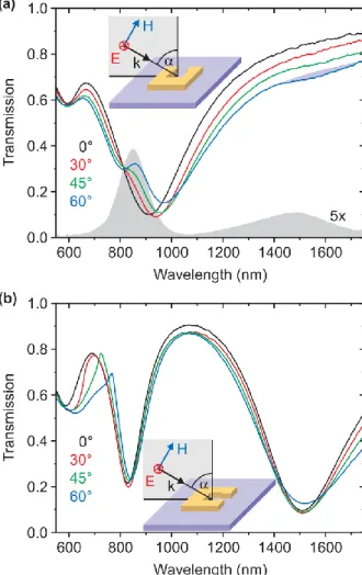
Enkrich et al. also fabricated arrays of Au split rings with a 50-nm minimum
normal-incidence conditions, they demonstrated the split rings exhibit a fundamental magnetic mode, arising from a coupling via the electric component of the incident light. For oblique incident light, a coupling via the magnetic component is demonstrated as well. Moreover, they identified a novel higher-order magnetic resonance at around 370 THz (800 nm wavelength) that evolves out of the Mie resonance for oblique incident light. Comparison with theory delivers good agreement and also shows that the structures allow for a negative magnetic permeability (Figure 2-4).
Figure 2-3 Electron micrograph of a split ring array. The lower right-hand side inset shows the dimensions of an individual split ring. The corresponding measured normal-incidence transmission and reflection spectra for horizontal and vertical polarization are shown in (b) and (c), respectively [3].
Figure 2-4 Measured transmission spectra taken for oblique incidence for the configurations shown as insets (whereα= 60o) [3].
(b) Metal Cut-Wire Pairs
The metamaterials which generate magnetic resonance are not only appeared in
the form of metal split-ring resonator. Grigorenko et al. made a critical step of demonstrating metamaterials with magnetic response by employing a novel geometry at frequencies in the visible spectrum (Figure 2-5) [5]. The metal cut-wire pairs exhibit a strong magnetic resonance at visible-light frequencies, including a band with negative permeability. The arising magnetism could be attributed to the excitation of an antisymmetric plasmon resonance. Their high-frequency results also revealed the feasibility of magnetic resonance at visible frequencies.
Figure 2-5 (a) Scanning electron micrograph (viewed at an angle) of an array of Au nanopillars. (b, c) Numerical simulation of the distribution of electric currents (arrows) inside a pair of such pillars for the symmetric and antisymmetric resonant z-modes, respectively [5].
2.1.3 Dielectric Nanoparticles
In 1983, Kerker et al. theoretically predicted another strong electromagnetic resonance effect for metamaterials: magnetic resonance. They proposed that hypothetical magneto-dielectric particles exhibiting both electric and magnetic dipole resonances with coherent effects would generate strong magnetic resonant phenomena [6]. This prediction opened a new course to realize negative permeability without metal metamaterials. The alternative approach achieving strong magnetic response with low losses is to use NPs made of high-refractive index dielectric materials.
Following the Mie theory of light scattering by a spherical NP, strong magnetic dipole resonance can be achieved in a particular parameter range.
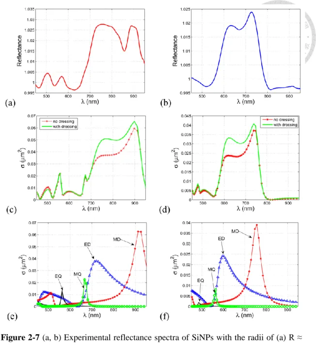
Experimental approaches have since been developed to demonstrate magnetic resonance generated from high-refractive-index dielectric and semiconductor NPs at optical and infrared frequencies. For example, Evlyukhin et al. experimentally demonstrated a strong resonant light scattering by individual spherical SiNPs [7]. The SiNPs are demonstrated their low-frequency resonance corresponds to the magnetic dipole resonance. Due to high permittivity, the magnetic dipole resonance is observed in the visible spectral range for SiNPs with diameters of 200 nm, thereby opening a way to the realization of isotropic optical metamaterials with strong magnetic responses in the visible region (Figure 2-6, 2-7).
Figure 2-6 SEM images of spherical SiNPss transferred onto a glass substrate (the images are taken at an angle of 45°). (a) R ≈ 131 nm, (b) R ≈ 104 nm. Insets are the corresponding dark- field images of the NPs [7].
Figure 2-7 (a, b) Experimental reflectance spectra of SiNPs with the radii of (a) R ≈ 131 nm and (b) R ≈ 104 nm located on a glass substrate with the refractive index n = 1.5. (c, d) Calculated scattering cross sections into the conical region with angle θ = 40° of SiNPs presented as a point multipole scatterers (electric dipole, magnetic dipole, electric quadrupole), and magnetic quadrupole located at the NP center in air.
Corresponding polarizabilities are taken from Mie theory for (c) R = 122 and (d) R = 97. (e, f) Contributions of the different multipoles to the calculated scattering cross sections for (e) R = 122 and for (f) R = 97 [7].
Recently, Zywietz et al. also used SiNPs having sizes of a few hundred nanometres to exhibit unique optical properties due to their strong electric and magnetic dipole responses in the visible range [8]. They demonstrated a novel laser printing technique for the controlled fabrication and precise deposition of SiNPs (Figure 2-8). These NPs have electric and magnetic dipole resonances in the visible spectral range, which can be used for the realization of efficient nanoantennas, nanoemitter and novel metamaterials (Figure 2-9).
Figure 2-8 Laser-printing process of SiNPs. (a) Schematic illustration of femtosecond laser printing of NPs. (b) SEM images of the target before and after NP-ejection process from the SOI substrate (scale bar, 400 nm). (c) Array of several hundreds of amorphous SiNPs (diameter of 160 nm) fabricated by this method and visualized with dark-field microscopy (scale bar, 20 mm). The insert shows a SEM image of a single SiNP in this array (scale bar, 200 nm) [8].
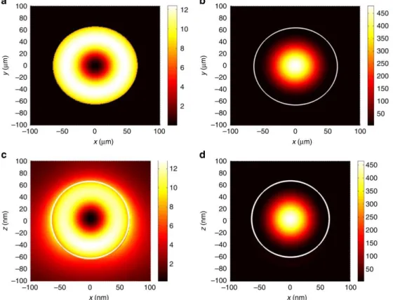
Figure 2-9 Distributions of electric and magnetic fields inside a SiNP. Electric (a) and magnetic (b) field intensities calculated inside the NP as a reaction on magnetic field.
Electric (c) and magnetic (d) field intensities calculated using Mie theory. The field intensities are presented in the cross-section of the NP with the radius of 65 nm. They are calculated in the plane perpendicular to the external magnetic field at the condition of magnetic dipole resonance. The white circles indicate the boundary of the NP [8].
Moreover, Kuznetsov et al. also demonstrated that SiNPs have strong magnetic dipole resonance, which can be continuously tuned throughout the whole visible spectrum varying particle size and visually observed by means of dark-field optical microscopy (Figure 2-10) [9]. These tunable resonance ranges opened up new perspectives for application of the resonant SiNPs.
Figure 2-10 Close-view dark-field microscope (i) and SEM (ii) images of the single NP. (a) to (f) correspond to six different NPs, respectively. (iii) Experimental dark-field scattering spectra of the NPs. (iv) Theoretical scattering and extinction spectra calculated by Mie theory for spherical SiNPs of different sizes in free space [9].
2.2 Surface-Enhanced Raman Spectroscopy
2.2.1 Background
Raman scattering, originated originating from the inelastic collisions between of photons and molecules, has attracted great attention since the its first observation in 1928 [10]. Typically, when photons collide with molecules without changing their frequencies during the collision but their pathways are altered. This kind of elastic collision is called “Rayleigh scattering.” On the other hand, when the inelastic collision between photons and molecules happens, the frequencies of photons shift accordingly. This “Raman scattering” provides the information of the bonding, symmetry, and vibration of the molecules, and therefore it is a potential analysis tool.
The probability of Raman scattering occurring is, however, extremely low, with only one Raman-scattering photon found among 10 million elastic collisions of Rayleigh-scattering photons. Due to the relatively weak intensity of Raman signals,
Raman spectroscopy was not a practical means of analysis until the development of SERS.
SERS is a technique that enhances the Raman signals of analytes. This technique was first developed by Fleischmann et al. in 1974 [11]. They found that the Raman signals of analytes were largely enhanced when the analytes were adsorbed on the rough surface of silver. SERS effects can enhance original Raman signals by several orders of magnitude, potentially extending the detection limit of Raman scattering down to the level of single molecules [12-13]. The stronger signals provided by SERS are generally resulted from mechanisms of electromagnetic and chemical enhancement [14]. Both will contribute to the total SERS enhancement, and it is not possible experimentally to make a clear separation of their individual contributions.
However, from a theoretical point of view one can identify at least four different situations where the SERS signal is enhanced due to a different mechanism (Figure 2-11) [15]: (a) Enhancement due to ground state chemical interactions between molecule and NP that are not associated with any excitations of the NP–molecule system. (b) Resonance Raman enhancement with the excitation wavelength being resonant with a molecular transition. (c) Charge-transfer resonance Raman enhancement with the excitation wavelength being resonant with NP–molecule charge-transfer transitions. (d) Enhancement due to a very strong local field when
the excitation wavelength is resonant with the plasmon excitations in the metal NP.
The first three contributions are often grouped together as the “chemical mechanism”
and the last is the “electromagnetic mechanism”. In a nutshell, Chemical enhancement is based on charge transfer between the analyte and the SERS-active substrate; it can enhance the Raman signals by one or two orders of magnitude.
Figure 2-11 Illustration of the different types of enhancement mechanism in SERS [15].
Electromagnetic enhancement is the dominant mechanism generally found on structured metal surfaces, especially on noble metal–based nanostructures. The plasmon excited on metal–based nanostructures will greatly enhance the electric field intensity nearby. Metallic nanostructures and NPs displaying surface plasmon resonance (SPR) or localized surface plasmon resonance (LSPR) effects in the visible or near-infrared (NIR) regime have been widely developed as SERS substrates [15–18].
2.2.2 Metal-Based SERS Substrates
As described in section 2.2.1, a large electromagnetic field will greatly enhance the Raman signals of analytes. Therefore, many efforts have been devoted into developing metal-based SERS substrates with the largest electromagnetic field intensity.
It is well-known that noble metallic NPs demonstrate LSPR phenomenon in the visible or NIR regime. Typically, the excitation light source in Raman measurement applies visible or NIR light lasers. Therefore, noble metallic NPs are the most popular choice for SERS substrates. Freeman et al. firstly proposed using a self-assembled metal colloid monolayer to be a SERS substrate [19]. The result is displayed in Figure 2-12. The number density of NPs can be controlled by the immersion time into the colloidal solution. A high coverage of NPs on the substrate will lead to many hot spots that greatly enhance the SERS signals.
Figure 2-12 Effect of Ag coating on the UV-VIS and SERS spectra of preformed Au colloid monolayers.[19].
After it is proved that the SERS signals of analytes will be enhanced by noble metallic NPs, many NP-based SERS substrates have been developed. For example, Lee et al. prepared Au NP arrays assembled on solvent-annealed block copolymer (polystyrene-b-poly(4-vinylpyridine), PS-b-P4VP) film [20]. By a solvent-annealing step, the P4VP domains became more regularly spaced and aligned perpendicular to the substrate. Upon immersion of the quaternized block copolymer film in a solution of citrate-stabilized gold NPs, self-assembly of the NPs into a hexagonal array commensurate with the array of P4VP domains was observed (Figure 2-13). Because the Au NP arrays on quaternized PS-b-P4VP films after different overgrowth times
demonstrated different diameters and gap spacers, the LSPR wavelength was finely tuned from 520 to 1000nm, and therefore it could be a broadband SERS substrate (Figure 2-14). However, the enhancement factor was only 105~106, and should be further optimized and improved.
Figure 2-13 (a) AFM image of the THF annealed PS-b-P4VP ordered film. (b–h) SEM images of Au NP arrays on the quaternized PS-b-P4VP films after different overgrowth times: (b) 0 min, (c) 1 minute, (d) 3 min, (e) 5 min, (f) 7 min, (g) 10 min and (h) 15 min [20].
Figure 2-14 SERS substrate enhancement factors as a function of overgrowth time and probing (incident) laser wavelength [20].
Besides, Yu et al. developed an eco-friendly paper substrate that provides extremely high SERS sensitivity as a result of the formation of metal NPs through a single-shot laser-induced photothermal effect (Figure 2-15) [21]. These characteristics allowed the SERS substrate to achieve detection limits down to the attomolar level—approaching single molecule detection after using a simple fabrication procedure (Figure 2-16).
Figure 2-15 Schematic representation of the fabrication of metal NPs on Si, glass, and paper by the laser-induced photothermal effect [21].
Ag
Si
few shots few shots
metal film deposition
metal film deposition
metal film deposition
few shots one shot
one shot
KrF KrF
KrF KrF
KrF glass
paper
Figure 2-16 SERS spectra of various concentrations of (a) R6G and (b, c) 4-ATP dried on (a, b) Ag and (c) Au NP–containing SERS filter paper, demonstrating attomolar detection ability [21].
In addition to the enhancements of the Raman signals of above molecules, previous literatures also presented using metal nanostructures enhanced the Raman signals of nearby graphene. Zhao et al. proposed a facile method for enhancing the Raman signals of as-grown graphene on Cu foils by depositing gold nanoislands onto the surface of graphene [22]. They found that an enhancement of up to 49 fold in the graphene Raman signal has been achieved by depositing a 4 nm thick Au film (as
1200 1250 1300 1350 1400 1450 1500 1550 0
2000 4000 6000 8000 10000 12000
1310
1507 10-6M
10-9M 10-12M 10-15M
Intensity (a.u)
Raman shift (cm-1) 1365
500 750 1000 1250 1500 1750 2000 0
2000 4000 6000 8000 10000 12000 14000 16000
1182 1590 1077
804 632
Intensity (a.u)
Raman shift (cm-1)
10-6M 10-9M 10-12M 10-15M 10-18M
x5 392
(a) (b)
500 1000 1500 2000 2500
0 1000 2000 3000 4000 5000 6000 7000 8000
Intensity (a.u.)
Raman shift (cm-1 )
4-ATP-10-6M 4-ATP-10-9M 4-ATP-10-12M 4-ATP-10-15M 4-ATP-10-18M 627 813
1077 1182
1590
(C)
shown in Figure 2-17). Through their simulations, the enhancement is considered to be related to the coupling between graphene and the plasmon modes of the coated Au nanostructures (Figure 2-18).
Figure 2-17 Raman spectra of graphene on Cu foils before and after depositing different thicknesses of Au films [22].
Figure 2-18 (a) Calculated absorbance of graphene/Cu and Au nanoislands/graphene/Cu hybrid systems with Au particle period p = 30 nm, diameter d = 24 nm and a graphene thickness of 1 nm. The inset shows the configuration of Au nanoislands/graphene/Cu for simulations. Simulated electrical field intensity
distributions in the (b) x–z plane and (c) x–y plane at z = 0 nm and z = 8 nm associated with the indicated positions in (a). In all field distribution images, the scale bar is 10 nm [22].
2.2.3 Metal-Free SERS Substrates
As described in section 2.2.2, metal-based SERS substrates display great enhancement of Raman signal. However, some metal-free enhancement methods have also been proposed to enhance Raman signals. For example, attenuated total reflection (ATR)–based Raman spectroscopy was first demonstrated by Ikeshoji et al. in 1973 [23]. They observe Raman scattering due to evanescent wave in total reflection. The authors measured the dependence of this intensity on the angle of incidence, which agrees with the inclination of the theoretical calculation. The total reflection Raman scattering spectra are shown in Figure 2-19, nevertheless, poor enhancement ability has limited the use of the ATR setup as a Raman signal enhancement technique.
Figure 2-19 Total reflection Raman spectra of the dependence of this intensity on the angle of incidence [23].
Besides, Alessandri applied TiO2 shell–based spherical resonator in the absence of plasmonic enhancers to enhance Raman scattering [24]. He demonstrated for the first time that a remarkable enhancement of Raman sensitivity can be obtained in the absence of plasmonic nanostructures by means of TiO2 shell-based spherical resonators (Figure 2-20). Evanescent electric fields generated through total internal reflection (TIR) within the dielectric micro-resonators generated local surface hot spots through whispering-gallery mode resonances. This effect can be exploited to fabricate a metal-free SERS active substrate (Figure 2-21).
Figure 2-20 (a) Scheme of preparation of TiO2 spherical resonators. The silica cores are conformally coated with an amorphous titania thin shell by atomic layer deposition. (b) SEM image showing a TiO2 spherical resonator. Surface fracture could see the SiO2 core and evaluate the thickness of the titania layer. Scale bar: 100 nm. (c) Low- and (d) high-magnification SEM images of TiO2 spherical resonators. Scale bars: 2 μm [24].
Figure 2-21 Raman spectrum of a 10−5 M MB solution adsorbed on a TiO2 spherical resonator substrate (T-rex100). The spectrum of the same solution adsorbed on a 100 nm-thick TiO2 planar film (multiplied by 4) is shown for a comparison [24].
Recently, Pirotta et al. also demonstrated that Raman scattering could be enhanced when the pump beam was coupled to Bloch surface waves in the purely dielectric multilayer configuration [25]. They demonstrated a lower bound for the SERS enhancement of 50 when the optical pump is resonantly coupled to the Bloch surface wave supported by the structure (Figure 2-22).
Figure 2-22 (a) Sketch of the typical multilayer supporting a Bloch surface wave. (b) Experimental configuration used in the angle-resolved attenuated total reflectance spectra [25].
Lee et al. also developed a reliable method to analyze these interference-enhanced Raman scattering (IERS) effect on graphene by considering the surface electric field, which can be calculated precisely by measuring the optical admittance of the thin- film assembly [26]. Besides, using this approach, they could enhance both the G and the 2D bands of graphene largely, uniformly, and equally, by
about 180 times relative to those obtained on a Si substrate. Under certain conditions, the Raman peak of graphene could even be enhanced by over 400 times (Figure 2-23).
Figure 2-23 Schematic representation and Raman spectra of graphene on the Si and one-dimensional photonic crystal substrates [26].
2.3 Photoluminescence of Silicon 2.3.1 Background
Because of bulk Si has both a relatively small and indirect band gap which prevents efficient interband radiative recombination, Si converts excited carriers to heat much more readily than to light. As a result of this main impediment to development of the Si for light-emitting devices, the use of optical data processing has not yet impacted chip-scale technology. This problem become more critical in not too distant future as the digital data technology industry moves to optical interconnects for board-to-board and chip-to-chip communications [27, 28].
To overcome this problem, the biggest challenge has been to develop an efficient Si-based light source. For this reason, room-temperature visible PL from porous Si

![Figure 2-11 Illustration of the different types of enhancement mechanism in SERS [15]](https://thumb-ap.123doks.com/thumbv2/9libinfo/9600344.628812/46.892.139.764.104.655/figure-illustration-different-types-enhancement-mechanism-sers.webp)
![Figure 2-14 SERS substrate enhancement factors as a function of overgrowth time and probing (incident) laser wavelength [20]](https://thumb-ap.123doks.com/thumbv2/9libinfo/9600344.628812/50.892.256.787.111.417/figure-substrate-enhancement-factors-function-overgrowth-incident-wavelength.webp)
![Figure 2-15 Schematic representation of the fabrication of metal NPs on Si, glass, and paper by the laser-induced photothermal effect [21]](https://thumb-ap.123doks.com/thumbv2/9libinfo/9600344.628812/51.892.169.790.109.543/figure-schematic-representation-fabrication-metal-induced-photothermal-effect.webp)
![Figure 2-19 Total reflection Raman spectra of the dependence of this intensity on the angle of incidence [23]](https://thumb-ap.123doks.com/thumbv2/9libinfo/9600344.628812/55.892.307.583.130.579/figure-total-reflection-raman-spectra-dependence-intensity-incidence.webp)
![Figure 2-23 Schematic representation and Raman spectra of graphene on the Si and one-dimensional photonic crystal substrates [26]](https://thumb-ap.123doks.com/thumbv2/9libinfo/9600344.628812/58.892.186.780.102.467/figure-schematic-representation-spectra-graphene-dimensional-photonic-substrates.webp)
