Research Express@NCKU - Articles Digest
Research Express@NCKU Volume 16 Issue 2 - November 19, 2010 [ http://research.ncku.edu.tw/re/articles/e/20101119/2.html ]
Investigation of thin-film type p-i-n ZnO-based light- emitting diodes
Ching-Ting Lee
Institute of Microelectronics, Department of Electrical Engineering [email protected]
NCKU Landmark Project《A009》
I
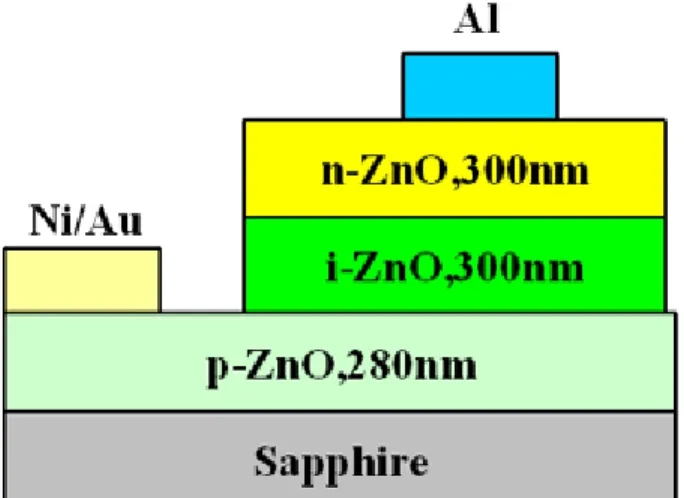
n this study, vapor cooling condensation system was used to implement the thin-film type ZnO-based p-i-n light-emitting diodes as shown in Fig. 1. In the vapor cooling condensation system, the material vapor gases were driven directly and deposited on the sapphire substrate using a pumping system. Because the sublimated materials were condensed and deposited by the cooling function of liquid nitrogen, the donor-like defect concentration could be quenched at the low temperature. The electron concentration and mobility for i-ZnO layer and n-ZnO layer were 7.6×1015 cm-3 and 6.0 cm2/V-s, and 1.7×1020 cm-3 and 3.1 cm2/V-s, respectively.Fig. 1. Structure of ZnO-based p-i-n LEDs
In order to fabricate the p-ZnO
film for the p-i-n light-emitting diodes, tungsten boats filled with the ZnO and LiNO3 powders, respectively, were heated in the vapor cooling condensation system simultaneously. Therefore, high quality LiNO3-doped ZnO (ZnO:LiNO3) film was obtained by the co-thermal
deposition of ZnO and LiNO3 powders. With an adequate post-annealing temperature in air ambience, the p-type conductive behaviors of ZnO:LiNO3 film could be achieved due to the activation of Li-N dual acceptor. The hole concentration and mobility of the p-type ZnO were 6.7×1017 cm-3 and 1.6 cm2/V-s, respectively. In order to fabricate the ohmic contact, Ni/Au (20/100nm) and Al (100nm) were deposited on the p-type ZnO layer and the n- type ZnO layer, respectively. Figure 2 shows the I•V characteristics of the ZnO p-i-n LEDs. A rectifying behavior for the p-type ZnO/i-ZnO/n-tpye ZnO (p-i-n) light-emitting diodes was clearly observed. The forward turn-on voltage and reverse breakdown voltage are about 2.5V and -7.5V, respectively. Figure 3 shows the output optical intensity as a function of wavelength for the room temperature electroluminescence (EL) spectrum of the ZnO p-i-n LEDs operated at 35 μA. The emission band centered at 388 nm is attributed to the near-band edge (NBE) emission of the i-ZnO film. The radiative recombination occurred in the i-ZnO region when the electrons and holes injected, respectively, from the n-ZnO film and p-ZnO layer and flowed into the i-ZnO film. Therefore, ZnO p-i-n light-emitting diodes can be obtained by using the vapor cooling condensation system.
1 of 2
Research Express@NCKU - Articles Digest
Fig. 2. Current-voltage characteristic of ZnO-based p-i-n LEDs
Fig. 3. Electroluminescence spectra of ZnO-based p-i-n LEDs
2 of 2