國 立 中 央 大 學
資 訊 工 程 學 系 碩 士 論 文
建構半導體晶圓針測圖樣分類辨識模型 Development Pattern Recognition Model for Classification of Circuit Probe Wafer Maps on
Semiconductor
指導教授 : 洪炯宗 博士 研 究 生 : 呂建鋒
中 華 民 國 101 年 5 月
國立中央大學圖書館 碩博士論文電子檔授權書
(100 年 9 月最新修正版)
本授權書授權本人撰寫之碩/博士學位論文全文電子檔
( )
(不包含紙本、詳備註 1 說 明),在「國立中央大學圖書館博碩士論文系統」。(以下請擇一勾選)
同意 ( )
(立即開放)
同意 (一年後開放),原因是:
( )
期刑投稿 同意
( )
(二年後開放),原因是:
同意 ( )
(三年後開放),原因是:
不同意
在國家圖書館「臺灣博碩士論文知識加值系統」
,原因是:
( )同意 ( )
(立即開放)
同意 (請於西元 2013 年 5 月 30 ( )
日開放) 不同意
以非專屬、無償授權國立中央大學圖書館與國家圖書館,基於推動「資源共享、
互惠合作」之理念,於回饋社會與學術研究之目的,得不限地域、時間與次數,
以紙本、微縮、光碟 及其它各種方法將上列論文收錄、重製、公開陳列、與發行,
或再授權他人以各種方法重製與利用,並得將數位化之上列論文與論文電子檔以 上載網路方式,提供讀者基於個人非營利性質之線上檢索、閱覽、下載或列印。
,原因是:
研究生簽名: 呂建鋒 學號:
論文名稱:
975302018
指導教授姓名:
建構半導體晶圓針測圖樣分類辨識模型
系所 :
洪炯宗 教授
資訊工程 所 博士班
備註:
碩士班
1. 本授權書之授權範圍僅限電子檔,紙本論文部分依著作權法第 15 條第 3 款之規定,採推 定原則即預設同意圖書館得公開上架閱覽,如您有申請專利或投稿等考量,不同意紙本上 架陳列,須另行加填聲明書,詳細說明與紙本聲明書請至 http://thesis.lib.ncu.edu.tw/ 下載。
2. 本授權書請填寫並親筆簽名後,裝訂於各紙本論文封面後之次頁(全文電子檔內之授權書
簽名,可用電腦打字代替)。
3. 請加印一份單張之授權書,填寫並親筆簽名後,於辦理離校時交圖書館(以統一代轉寄給
國家圖書館)。
4. 讀者基於個人非營利性質之線上檢索、閱覽、下載或列印上列論文,應遵守著作權法規定。
I
建構半導體晶圓針測圖樣分類辨識模型 Development Pattern Recognition Model for Classification of Circuit Probe Wafer Maps on
Semiconductor
研究生 : 呂建鋒 指導教授 : 洪炯宗 博士 國立中央大學 資訊工程研究所
在半導體業界中,晶圓針測 (Circuit Probe) 屬於生產過程中的後段測試,其 測試結果包含了晶圓良率的好壞及追溯異常製程與設備所需之重要資訊,並且產 生圖形化的故障圖樣分佈於晶圓上,此資訊為製程錯誤診斷及機台故障檢視提供 很多有用的線索。因此,了解晶圓針測圖樣所代表的意義及造成故障圖樣的原 因,在工程資料關聯性分析中是件非常重要的工作。為了減少以往人為檢視方式 所消耗的時間,一個準確的晶圓自動化分類系統在工程資料分析中是不可或缺的 一套工具。本論文使用影像處理中偵測直線之霍夫轉換(Hough transform)及偵測 圓形之圓形霍夫轉換(Circular Hough transform)演算法擷取直線及圓形分佈故障 圖樣之特徵,並且使用了數種常見的特徵擷取技巧來取得其它不同的故障圖樣。
研究中提出一套結構化系統,將晶圓特徵擷取出後透過數種資料探勘分類演算法 建立不同的分類器(classifier),並且驗證所提出之數種特徵可有效消除雜訊對晶 圓分類準確度的影響。最後以實際半導體資料及模擬資料評估不同資料勘分類演 算法對於本研究所提出的特徵擷取方法有最佳的準確度。
摘要
II
Development Pattern Recognition Model for Classification of Circuit Probe Wafer Maps on
Semiconductor
Student: Chien-Feng Lu Advisor: Dr. Jorng-Tzong Horng
Institute of Computer Science and Information Engineering, National Central University, Taiwan
Abstract- Circuit probe test is an end of line testing that the individual die has been measured at wafer level in modern semiconductor manufacturing. The test results are visualized as a spatial distribution of the failures on the wafer which can provide some valuable information for the production of failures. In order to reduce time consumption by human operation, a great accuracy of automatic classification system is clear needed for engineering analysis. In this paper, we demonstrate how a robust feature extraction procedure using by classical Hough transform (HT) and circular Hough transform (CHT) can be adapted to detect lines and rounds spatial patterns on circuit probe wafer map. In addition, we also used several technique to detect others spatial patterns. These features which are effectively eliminate the influence of noise to perform pattern classification. The presented methodology is validated with real fabrication data and several data mining classification algorithms are presented to evaluate the advantage of this methodology.
Abstract
Keywords - semiconductor wafer classification, circuit probe test, features extraction, Hough transform, data mining
III
Table of Contents
摘要... I Abstract ... II
Chapter 1 Introduction ... 1
1.1 Background ... 1
1.2 Motivation ... 2
1.3 Goals ... 3
Chapter 2 Related Works ... 4
2.1 Introduction to semiconductor manufacturing ... 4
2.1.1 Semiconductor process sequences ... 4
2.1.2 Circuit probe maps ... 6
2.2 Literature review ... 10
2.3 Related tools... 14
2.3.1 Noise reduction ... 14
2.3.2 Canny edge detector ... 17
2.3.3 The Hough Transform ... 19
2.4 Classification of data mining ... 23
2.4.1 10-fold cross-validation ... 25
2.4.1 Classification algorithms ... 27
2.5 The WEKA data mining workbench ... 31
Chapter 3 Materials and Methods ... 32
3.1 Materials ... 32
3.2 System flow ... 34
3.3 Methods... 34
3.3.1 Pattern definition ... 34
3.3.2 Data preprocessing ... 35
3.3.3 Feature extraction ... 37
Chapter 4 Results ... 46
4.1 Implementation ... 46
4.2 Classification results ... 50
Chapter 5 Discussion ... 53
Reference ... 54
Appendix ... 56
IV
List of Figures
Figure 1.1 Diagram of our goal... 2
Figure 2.1 Block diagram representation of a manufacturing system ... 4
Figure 2.2 Semiconductor manufacturing process flow ... 5
Figure 2.3 Wafer level testing ... 6
Figure 2.4 The CP map draw in different color with bin number ... 7
Figure 2.5 The CP map draw in black with fail bin ... 7
Figure 2.6 The CP yield trend chart ... 8
Figure 2.7 The CP wafers of low yield lot (LOT0032)... 9
Figure 2.8 The CP wafers of low yield lot (LOT0051)... 9
Figure 2.9 The spatial pattern separated into systematic and random fails ... 15
Figure 2.10 The 3x3 and 5x5 mask ... 15
Figure 2.11 The 3x3 mask overlap on partial of wafer map ... 16
Figure 2.12 Image edge detection using OpenCV ... 18
Figure 2.13 The Hough transform process... 19
Figure 2.14 The linear Hough transform ... 20
Figure 2.15 Points are located on the same perimeter ... 22
Figure 2.16 Train and Test method ... 24
Figure 2.17 10-fold cross-validation ... 26
Figure 2.18 Example of decision tree using WEKA ... 28
Figure 2.19 The generative process by NBC ... 29
Figure 2.20 General framework of bagging ... 29
Figure 2.21 Boosting illustration ... 30
Figure 2.22 The WEKA explorer interface ... 31
Figure 2.23 The WEKA experimenter interface ... 32
Figure 3.1 The EDA database in semiconductor industry ... 33
Figure 3.2 System flow ... 34
V
Figure 3.3 Pattern definition ... 35
Figure 3.5 Filter origin map ... 36
Figure 3.6 The result of an edge recognition procedure in a sample wafer ... 37
Figure 3.7 Line detection of Hough transform ... 37
Figure 3.8 Four angle line detection of Hough transform ... 38
Figure 3.9 Linear Hough transform for variant shape ... 39
Figure 3.10 Circle detection using circular Hough transform ... 40
Figure 3.11 Finding optimal CR ... 41
Figure 3.12 Circle detection in Ring and Blob spatial pattern ... 42
Figure 3.13 The distance of Bull eye and Blob spatial pattern ... 43
Figure 3.14 Wafer splitting ... 43
Figure 3.15 Failed ratio in zone ... 44
Figure 4.1 System interface I ... 46
Figure 4.2 System interface I ... 47
Figure 4.3 System interface II ... 47
Figure 4.4 System interface III ... 48
Figure 4.5 Training in WEKA data mining tool... 49
Figure 4.6 The result of system ... 49
Figure 4.7 Mixture spatial pattern ... 52
VI
List of Tables
Table 2.1 The comparisons between presented methodologies. ... 13
Table 2.2 The function of Canny in OpenCV ... 18
Table 2.3 An example accumulator ... 22
Table 3.1 The EDA database in semiconductor industry ... 33
Table 3.2 Relationship between features and patterns ... 45
Table 4.1 The accuracy for simulated dataset ... 51
Table 4.2 The accuracy for manufacturing dataset ... 51
1
Chapter 1 Introduction
1.1 Background
The semiconductor manufacturing has been became a more highly complex technology which involving a series of precise arrangement of process steps through several processing equipments to produce hundreds of individual integrated circuit die on a piece of silicon wafer. Thus, any tool excursion can lead to a yield loss across the industry. Such losses can originate from different kinds of problems which may arise from equipment malfunctions, delicate and difficult processing steps, or human mistakes [1]. In order to be competitive in the semiconductor manufacturing industry, the detection of these problems becomes a critical issue because yield performance is closely related to the control and efficiency of the wafer manufacturing process.
Therefore, the yield enhancement engineering usually focuses on the investigation of low-yield lots, the elimination of defects, process excursions, the correlation between electrical and functional experiment result, and the improvement of baseline product yield [2, 3].
Some process step faults are detectable only by end-of-line tests. It is well know that spatial patterns in the distribution of Circuit Probe (CP) failures on a wafer can be related to the potential causes in end-of-line tests. If the dies that fail at CP tests are visualized as black pixels, the spatial distribution of the failures is likely to show characteristic patterns. Different shapes are possible in Line, Bull eye, Ring, Blob, and Edge. From these patterns it may be possible to understand which type of problem
originated the failures, in which step of the process, and in which equipment.
Therefore, these patterns can be used to trace back to the problems that originated the failures either by analyzing their qualitative features or by correlating them with the
2
lot history [1, 4]. Thus, engineers are usually screen form CP wafer map to conduct through statistical data analysis for fault diagnosis. Since there is a lot of data produce by step of process and equipment every day. For this reason, it is needed to develop a fully automatic classification system to screen signatures for engineers on CP wafer maps without time consuming and perform yield prediction, fault diagnosis, correcting manufacturing issues and process controls as shown in Figure 1.1.
Figure 1.1 Diagram of our goal
1.2 Motivation
In previous researches, there are many proposed methods intend to classify and recognize these kinds of spatial patterns such as statistical distribution analysis, neural networks and image processing. Although many of these methods are powerful, they are generally unable to extract meaningful data or failed to detect noisy datasets. A more robust classification scheme can be achieved using data mining algorithms.
However, the accuracy and reliability of the data mining approach depends on features selection and the selected features must have some unique attribute that can be used to discriminate each characteristic pattern [8]. As exhaustive search technique,
3
the Hough transform is a robust method which is relatively unaffected by noise for feature detection and generally been recognized as a reliable for linear and circular object detection [14]. K. Preston White et al. have been demonstrated how this transform can be adapted to classify signatures on semiconductor wafers in 2008 [5], but the procedure does not appear to be as useful for detecting patterns in Bull eye and Blob. Thus, we future apply circular Hough transform to detect spatial pattern
representing in Bull eye and Blob.
Otherwise, we found that some of these methods analyzed in rarely dataset. It appears very difficult to define conclusions on the relative performance on the basis of such limit dataset. For this reason, we analyzed much more extensive actual data provided by engineering database in a famous semiconductor company and simulated sufficient coverage of each spatial patterns generated by artificiality.
1.3 Goals
We intended to develop a pattern recognition model with a set of features and demonstrated this model is more accurate and reliable. Otherwise, we want to train and evaluate this model with sufficient actual data. In order not to against specific company and area, we further generated simulated data by artificiality. We hope that the accuracy on simulated data will consistent with real manufacturing data.
4
Chapter 2 Related Works
2.1 Introduction to semiconductor manufacturing
In this section, we provide an overview of semiconductor manufacturing. As illustrated in Figure 2.1, the manufacturing operation can be viewed graphically as a system with raw materials and supplies as its inputs and finished commercial products as outputs. The input materials include semiconductor materials, dopants, metals, and insulators. The corresponding outputs include integrated circuits, IC packages, printed circuit boards, and ultimately, various commercial electronic systems and products.
Figure 2.1 Block diagram representation of a manufacturing system
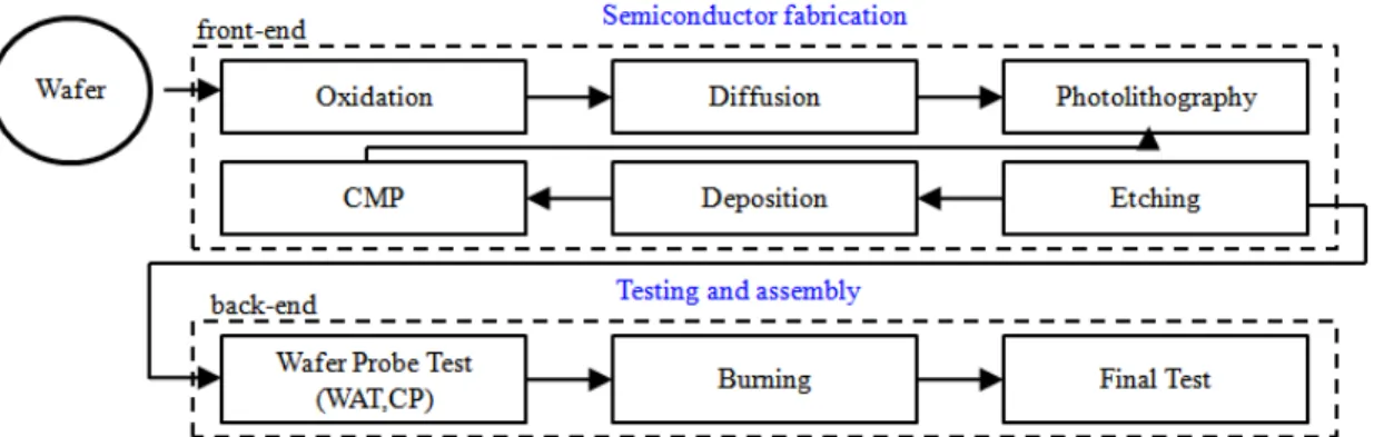
The types of processes that arise in semiconductor manufacturing include crystal growth, oxidation, photolithography, etching, diffusion, ion implantation, planarization, and deposition processes. Viewed from a systems-level perspective, semiconductor manufacturing intersects with nearly all other IC process technologies, including design, fabrication, integration, assembly, and reliability. The end result is an electronic system that meets all specified performance, quality, cost, reliability, and environmental requirements [21].
2.1.1 Semiconductor process sequences
Semiconductor manufacturing consists of a series of sequential process steps like
5
the one described in the previous section in which layers of materials are deposited on substrates, doped with impurities, and patterned using photolithography to produce ICs. Figure 2.2 illustrates the interrelationship between the major process steps used for semiconductor fabrication. Polished wafers with a specific resistivity and orientation are used as the starting material.
Figure 2.2 Semiconductor manufacturing process flow
The process sequences of semiconductor can roughly be divided into front-end and back-end processing. The front-end processing includes oxidation, photolithography, diffusion, etching, thin-film deposition, and chemical mechanical polishing. After processing, each wafer contains hundreds of identical rectangular chips (or dies). The back-end processing includes test and assembly. Before the identical rectangular chips assembled into a package, functional test is performed.
Functional testing at the completion of manufacturing is the final arbiter of process quality and yield. The purpose of final testing is to ensure that all products perform to the specifications for which they were designed. For integrated circuits, the test process depends a great deal on whether the chip tested is a logic or memory device.
Circuit Probe test is a kind of wafer probe test when the polished wafer finished from semiconductor fabrication [21].
6
2.1.2 Circuit probe maps
Testing the individual die at the wafer level has been an integral part of the semiconductor manufacturing process, it is so-called wafer probe or wafer sort. Figure 2.3 is a picture of a typical probe test cell including the Automatic Test Equipment (ATE) and a wafer prober which is a machine used to test integrated circuits. The prober holds the wafer being tested on a vacuum chuck. The chuck moves in the horizontal x-y directions positioning the individual die on the wafer in the center of the test head. The prober Interface Board (PIB), sometimes called the DUT Load Board, connects the bottom side of the test head. Below the PIB, in the stack of tooling underneath the test head, is the Spring Contactor Assembly. The PIB is hard-mounted to the prober, so the Spring Contactor Assembly must provide a little vertical compliance and theta rotation as well as routing the test signals. The bottom element in the stack is the probe card. It has connectors or pads on the top side mating to the Spring Contactor Assembly and needles on the bottom side that physically contact the I/O pads on the individual die being tested [22].
Figure 2.3 Wafer level testing [22]
When all test patterns pass for a specific die, its position is remembered for later
7
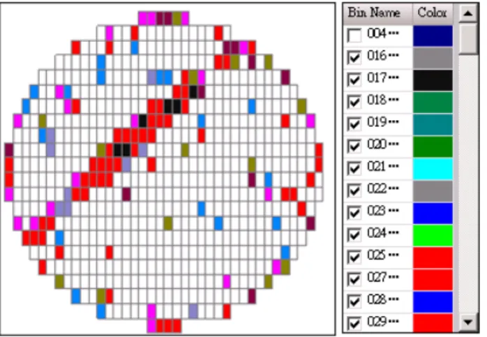
use. Sometimes a die has internal spare resources available for repairing. Non-passing circuits are typically marked with a small dot of ink in the middle of the die, or the information of passing/non-passing is stored in a file, such a file recorded the result of the electrical test information on the wafer and can be drawn by visualized map. This wafer map categorizes the passing and non-passing dies by marking use of bins. A bin number is then defined as a good or bed die as shown in Figure 2.4.
Figure 2.4 The CP map draw in different color with bin number
If the dies that fail at probe tests are visualized as black pixels, the spatial distribution of the failures is likely to show characteristic patterns as shown in Figure 2.5.
Figure 2.5 The CP map draw in black with fail bin
Because of some process step faults are detectable only by end-of-line tests and spatial patterns in the distribution of Circuit Probe failures on a wafer can be related
8
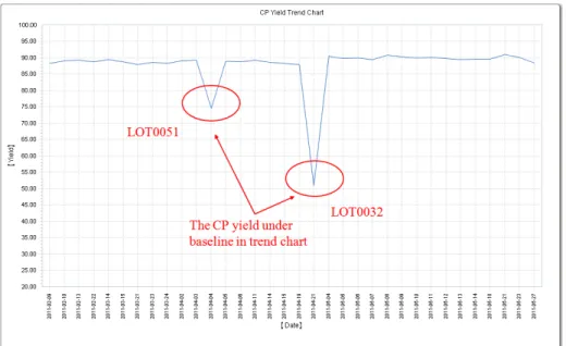
to the potential causes in end-of-line tests. From these patterns it may be possible to understand which type of problem originated the failures, in which step of the process, and in which equipment. Therefore, these patterns can be used to trace back to the problems that originated the failures either by analyzing their qualitative features or by correlating them with the lot history. For instance, consider the plot in Figure 2.6 in which the average lot-level CP yield of a quarter of certain product. It can be found that the yield of two lots named LOT0032 and LOT0051 were significantly lower than baseline of specific value. After identified these low yield lots, the engineers will further go to examine CP maps by wafer in these lots.
Figure 2.6 The CP yield trend chart
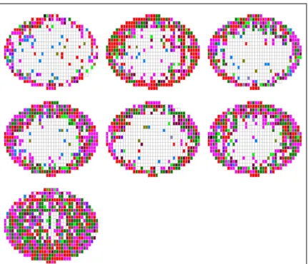
In Figure 2.7, the CP maps present 6 wafers from the lot of LOT0032. It is easily to find out that all wafers failed in edge spatial patterns.
9
Figure 2.7 The CP wafers of low yield lot (LOT0032)
Besides, in Figure 2.8, the CP maps present 25 wafers from the lot of LOT0051.
It is also easily to find out that most wafers failed in center spatial patterns.
Figure 2.8 The CP wafers of low yield lot (LOT0051)
Because of spatial patterns are usually due to process errors and tool excursions
10
can be extremely valuable to engineers when identifying root cause in their work.
Therefore, engineers are often screen form CP wafer map to conduct through statistical data analysis for fault diagnosis. Since there is a lot of data produce by step of process and equipment every day. For this reason, it is needed to develop a fully automatic classification system to screen signatures for engineers on CP wafer maps without time consuming and perform yield prediction, fault diagnosis, correcting manufacturing issues and process controls.
2.2 Literature review
In the past few years, methods of automated spatial pattern analysis in the semiconductor manufacturing process have been widely investigated and discussed.
They proposed many approaches to classify and recognize these kinds of spatial patterns. At least four different approaches are possible, the simplest and least efficient is visual classification performed by a human operator. In view of the time needed to analyze thousands of wafers, it is not possible to have a fast feedback to correct problems. The second approach is statistical distribution analysis such Poisson or negative-binomial distributions are normally on lot-level basis for account for cluster phenomena. For example, Friedman et al., developed statistics measuring spatial dependency of defects to detect systematic clustering [11]. Although most statistical approaches are able to detect anomalies on wafer, they are generally unable to extract meaningful data from the spatial pattern since tend to incorrectly assume a stationary probability distribution. Systematic spatial patterns caused by the semiconductor fabrication process involve a complex variation of statistical parameters which are highly dependent on the process, machine, suppliers, materials etc. Thus, traditional statistical approaches are not recommended for practical application. Moreover, the monitoring statistics often bear relatively complex
11
statistical properties, adding difficulty in implementation of these methods. The third approach is neural network algorithms that can recognize spatial patterns. However, the major limitation of neural-network approaches lies in its inability to classify two or more shift variance in the spatial patterns. It is also incapable of detecting the presence and location of a cluster. Many of these methods need a large training dataset, and due to the complexity of the algorithms, most of these methods do not provide a statistically rigorous evaluation of their performances in pattern detection. The fourth approach is image processing, this method attempts to detect cluster outliers, but fall sort at detecting real manufacturing spatial pattern, which are almost always of different and imperfect geometrical shapes. However, this approach lacks flexibility because it requires the prior knowledge of all the possible shapes in different products and difficult to predict in advance [23, 24, 25]. Image processing and artificial neural network (ANN) classification approaches are notorious to fail for noisy datasets.
Generally, neural network approaches cannot identify two or more shift variant or rotational variant spatial patterns that belong to the same defect pattern type [8].
A more robust classification scheme can be achieved using data mining algorithms. However, the accuracy and reliability of the data mining approach depends on features selection and the selected features must have some unique attribute that can be used to discriminate each characteristic pattern. As exhaustive search technique, the Hough transform is a robust method which is relatively unaffected by noise for feature detection and generally been recognized as a reliable for linear and circular object detection [14]. The Hough transform employing a normal line-to-point parameterization is widely applied in digital image processing for feature detection. It is a very powerful tool for the detection of parametric curves and generally used to detect lines and rounds, which is originally proposed by Hough in 1959. The advantage of Hough transform is as follows: it isn’t sensitive to the noise of
12
image, effectively eliminate the influence of noise. The transform is convenient to parallel computing. In the field of computer vision, some issues are complex and require a great of computation, and parallel computing is used by modified Hough transform, and then calculating the start and end of the line. In this paper, we applies the Hough transform for spatial pattern recognition and a frequency count to indentify lines or sets of lines which represent line signatures. K. P. White et al. have been demonstrated how this transform can be adapted to classify signatures on semiconductor wafers in 2008 [5], but the procedure does not appear to be as useful for detecting spatial patterns in Bull eye and Blob. Thus, we future apply circular Hough transform to detect spatial pattern representing in Bull eye and Blob which is proposed to detect rounds for spatial pattern [5, 6].
However, we found that some of the previous methods analyzed in rarely dataset.
For instance, on the basis of the analysis of simulated and real wafers, Chen and Liu concluded that the ART1 network classifies can recognize the similar defect spatial patterns more easily and correctly. However, the simulated data set was made of only 35 simulated wafers, each of which containing 294 dies. As for the patterns, there are three types of rings and four types of scratches. The real wafers analyzed in the paper were only 14 wafers, still with 294 dies per wafer [2]. L.J. Wei using neural network approaches for recognizing the bin-map patterns on the wafer. In their work, the 57 actual wafers had been analyzed which included 9 Bull eye, 14 Edge, 9 Blob, 9 Ring and 16 Line spatial patterns [12]. S.F. Liu et al. proposed a feature extraction procedure based on wavelet transform to extract features that represent different defect patterns. The presented methodology is verified with real industrial data from a semiconductor company and the experimental results show the presented methodology is able to recognize defect patterns with recognition accuracy of 95%, however, the real industrial data also made of only 65 wafers and the system failed to
13
recognize Blob type of spatial pattern [25]. It appears very difficult to define conclusions on the relative performance on the basis of such limit dataset [20]. For this reason, in this paper we analyzed much more extensive sets of manufacturing data provided by engineering database in a famous semiconductor company and sufficient coverage of simulated data generated by artificiality. Table 2.1 illustrates the comparisons between previous methodology with accuracy and data set.
Table 2.1 The comparisons between presented methodologies.
Literature
Feature selection method
Pattern Data set Accuracy
F.L. Chen and S.F. Liu, A neural-network approach to recognize defect spatial pattern in
semiconductor fabrication, 2000
-- line, ring 14 real data 60%
K.P. White et al., "Classification of defect clusters on semiconductor manufacturing wafers via the Hough
transform", 2005
Linear Hough transform
bull eye, edge, ring and line
-- --
L.J. Wei, "Development of wafer bin map pattern recognition model - using
neural network approach", 2006
5 features
bull eye, edge, blob, ring and line
57 real data 93.75%
S.F. Liu et al.,"Wavelet transform based wafer defect map pattern recoginition system in semiconductor
manufacturing", 2008
Wavelet transform
line, blob, ring, radial, repeat
65 real data 60%~100%
J.W. Cheng et al., "Evaluating performance of different classification
algorithms for fabricated semiconductor wafers", 2010
2 features
bull eye, edge, blob, ring and line
unknown 0%~100%
Based on this automatic classification methodology, we could obtain the information on problems related to the signature maps. Finding a process root cause is
14
not an easy task. Thus, a greater accuracy of classification is needed for engineering analysis. Subsequently, the process history of each wafer is used to create a list of the process step and keep track of which equipment must be responsible the problem in analysis. This paper proposed the use of five types of features from the semiconductor CP map on the wafer and evaluates the performance of several classification algorithms. We will demonstrate that the result present in more high accuracy with sufficient coverage of data set.
2.3 Related tools
The Computer sciences are suitable implement for pattern analysis because they provide the ability to promptly perform systematic, repetitive analyses on large data sets. It is a significant challenge to analyze huge quantities of wafer inspection and electrical test data and extract the information needed for identifying yield improvement opportunities [7]. There are some techniques used in our methodology that we talk about as following section. For feature selection, it is including noise reduction, image edge detection, Hough transform. For evaluation, we verify the accuracy with data mining algorithms.
2.3.1 Noise reduction
In general, the spatial pattern composed of systematic and random fails as shown in Figure 2.9. The random fails are most often produced by the clean room environment and can only be reduced through a program of long term. Because of random fails have useless information for yield improvement, thus, we do not discuss this kind of fails in this paper. On the contract, systematic fails are often caused by some kind of machine failures and process-related fails are often caused by one or
15
more process steps not meeting the required specifications. Therefore, it is important to routinely monitor by systematic fails of wafer yield for irregularities. The segmentation is done on a by wafer basis and we will demonstrate the results in chapter 3.
Figure 2.9 The spatial pattern separated into systematic and random fails
In order to generating smoothed wafer maps without random fails, we applied an approach called local kernel estimator defined by D. J. Friedman et al. in 1997 [11].
The goal of the smoothing operation is to highlight regions with a large number of fail chips. As a visual process, this identification involves judging how closely the numbers of fail chips in small area agree with what might be expected by considering the yield of the wafer as a whole. To be more precise, at each chip position, we consider a neighborhood around the given chip and calculate the proportion of the chip’s neighbors that are failed. The choice of the neighborhood is flexible, although in practice we have typically employed 3x3 or 5x5 neighborhoods as shown in Figure 2.10.
Figure 2.10 The 3x3 and 5x5 mask
16
Further, one could use a weighted average with some specified set of weights instead of simple proportion. Essentially, the proportions are transformed to values between zero and one by applying a sequence of transformation, a variance-stabilizing transformation followed by centering and scaling a finally probability-integral transformation. Toward this end, local kernel estimator had been defined as:
Where Ni is the chip set adjacent with i, Wi(j) is the weight of the chip j and IF(j) is indicate the chip j is failure or not. When the chip was failed the value would be denoted as 0, otherwise the value would be denoted as 1. In the previous research [12], the weight of mask has been design in 3x3 mask. Inside the mask, the weight of center die I (Wi) is set as , and the weight of J (Wj) is set as . For instance, when 3x3 mask overlap on a partial of wafer map as shown in Figure 2.11, they can be calculated in following statement:
Figure 2.11 The 3x3 mask overlap on partial of wafer map
After we calculated for all of the dies on the wafer we could realize that will
17
change by yield of the wafer, thus we transfer by the below formula:
Because of the edge dies don’t have completed neighborhood then we transferred these edge dies by Standard normal integral function to solve it. In general, we don’t try to integrate it, just use the standard normal cumulative probability table as shown in chapter appendix.
2.3.2 Canny edge detector
Edge detection is a basic tool in image processing and computer vision, especially in the areas of feature detection and feature extraction, which aim at identifying points in a digital image at which the image brightness change sharply discontinuities. Typically, the first step in the process is to perform some detector of edge detection on the image, and to generate a new binary boundary image that provides the necessary segmentation of the origin image. The edge detection is a very important process required for the Hough transform because it could reduce the computation time and has interesting effect of reducing the number of useless vote.
Many edge detection methods have been applied for different application. Among them, the Canny edge detector is the boundaries separating regions with different brightness or color suggested by J. Canny in 1886 which is an efficient method for detecting edges. It takes grayscale image on input and returns bi-level image where non-zero pixel mark detected edges [15].
In this paper, we applied the Canny function provided by OpenCV (Open Source Computer Vision Library) which is a library of programming function at real time
18
computer vision, developed by Inter corporation. The document of function is shown in Table 2.2.
Table 2.2 The function of Canny in OpenCV
The Canny algorithm is adaptable to various environments and its parameters allow it to be tailored to recognition of edges of differing characteristics depending on the particular requirements of a given implementation [13]. Otherwise, Canny detector gives thin edge compared to Sobel detector as shown in Figure 2.12.
Figure 2.12 Image edge detection using OpenCV (a) origin image (b) Canny (c) Sobel
19
2.3.3 The Hough Transform
The Hough Transform is an algorithm presented by Paul Hough in 1962 for the detection of features of a particular shape like lines or circles in digitalized images in image analysis, computer vision and digital image processing. It can be applied to many computer vision problems contain feature boundaries which can be described by regular shapes. The purpose of the technique is to find uncompleted objects by voting procedure. This voting procedure is carried out in a parameter space, from which object candidates are obtained as local maxima in as so-called accumulator space that is explicitly constructed by the algorithm for computing the Hough transform. The classical Hough transform was concerned with the identification of lines, but later the Hough transform has been extended to identify of other shapes, most commonly circles or ellipse. The main advantage of the Hough transform technique is that it is tolerant of gaps in feature boundary descriptions and is relatively unaffected by image noise. Figure 2.13 shows the diagram of Hough process [14, 15].
Figure 2.13 The Hough transform process
A. Line detection
20
The simplest case of Hough transform is the linear transform for detecting straight lines. In the image space, the straight line can be described in rectangular coordinate xy-plane (image space) as follows:
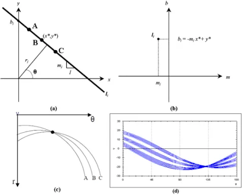
y = mx + b
where m and b are the slope and intercept of line lj, as shown in Figure 2.14(a). The line in the xy-plane can be transformed into the slope-intercept parameter plane as follows:
b = -xm + y
This line-to-point transformation is the basis for its usefulness, as shown in Figure 2.14 (b).
Figure 2.14 The linear Hough transform (a) Line lj trhough the fixed point (x*, y*) in the xy-plane (b) a single point (mj, bj) in the slope-intercept parameter plane (c) 3 points in the same line in image space transformed into r-θ parameter space and intersect to a point (d) A real case transformation in r-θ parameter space
The drawback of the (m, b) parameterization is that when lines which are nearly vertical in the xy-plane have extremely large values for both m and b. Thus, an
21
alternate parameterization was employed to avoid this shortcoming which called r-θparameter space as follows:
x cosθ + y sinθ = r
Every point in the same line in the image space will intersect to a point in the r-θ parameter space, as shown in Figure 2.14 (c), which makes the lines extraction problem transform to counting problem. A real case transformation from image space to r-θparameter space look likes Figure 2.14 (d).
Given this characterization of a line, we can then iterate through any number of lines that pass through a given point. We incorporate the results in an accumulator array. At the beginning, the accumulator array is initialized to zero for all cells. After that, for every value of A with a corresponding value B, the value of that cell is incremented by one [5, 14].
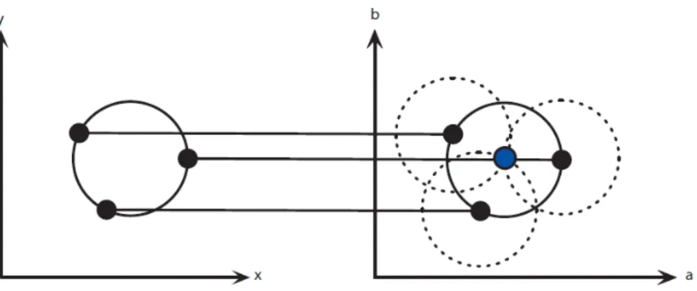
B. Circle detection
The Hough transform can also be used for detection circles and other parametric geometric figures. The circle is simpler to represent in parameter space, compared to the lines, since the parameters of the circle can be directly transfer to the parameter space as following:
r2 = ( x – a ) 2 + ( y – b ) 2
where a and b are the center of the circle in the xy-plane and where r is radius. The parametric representation of the circle is:
x = a + r cosθ y = b + r sinθ
At each edge point we draw a circle with center in the point with the desired radius. This circle is drawn in the parameter space, when the edge points in the
22
xy-plane are located on the same perimeter then the circles with center in these points
must be intersected to a point, as shown in Figure 2.15.
Figure 2.15 Points are located on the same perimeter
At the coordinates which belong to the perimeter of the drawn circle we increment the value in our accumulator matrix as show in Table 2.3. In this way we sweep over every edge point in the input image drawing circles with the desired radii and incrementing the values (or score) in our accumulator. When every edge point and ever desired radius is used, we can turn our attention to the accumulator. The accumulator matrix which is three dimensional, if the radius is not held constant, can quite fast grow large. In order to simplify the parametric representation of the circle, the radius can be limited to number of known radii, such as 1 < r < R where R is the wafer radius [16, 17].
Table 2.3 An example accumulator
index a b r score
1 23 4 5 17
2 26 9 8 15
3 23 5 5 15
4 24 5 5 13
5 30 4 12 13
6 25 2 7 13
… … … … …
23
2.4 Classification of data mining
Most of the machine learning used in data mining can be divided into supervised learning and unsupervised learning. Unsupervised learning refers to the problem of trying to find hidden structure in unlabeled data. The idea is to use algorithms that automatically identify the classes of patterns in the data set and assign each wafer to one of the classes. The advantage of unsupervised learning is the method can identify unsuspected patterns that could have been ignored by a human operator. Otherwise, the disadvantage is the lack of direction for the learning algorithm and that there may not be any interesting knowledge discovered in the set of features selected for the training. In supervised learning, each example is a pair consisting of an input object and a desired output value. A supervised learning algorithm analyzes the training data and produces a classifier. The classifier should predict the correct output value for any valid input object. For instance, a set of wafers is classified by a human operator and then used to train a classification model. More precisely, the parameters of the model are tuned until corresponded by the training set and classifies the data as correctly as possible. The idea is that when new wafers are presented to the trained model, the will be classified correctly. A major disadvantage of supervised learning is the time spent by a human operator in order to prepare the training set and the subjectivity of the classification carried out by the human operator, which could affect in an unpredictable way the final performance of the classifier. In other words, the advantage of supervised learning is that all separate classes in the algorithms are meaningful to humans [20]. Supervised learning algorithms are applied in this paper because the input-output relationship is known. We cannot do classification without labeled data because only the labels tell what the classes are. Many situations present hung volumes of raw data, but assigning classes is expensive because it requires
24
human insight.
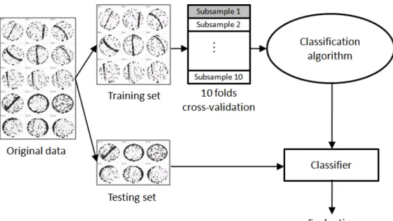
The methodology must be capable of mapping the features which are extracted from the input to the output. A so-called train and test method is used to construct a classifier in which the available dataset is divided into a training set and a test set, as show in Figure 2.16 [8]. The original data has been divided into training set and testing set. The training set used to train a classified model by data mining classification algorithm with 10-folds cross-validation. Once the classified model had been constructed, the testing set will applied to estimate the accuracy of classifier.
Figure 2.16 Train and Test method
It is natural to measure a classifier’s performance in terms of the error rate. The classifier predicts the class of each instance. If it is correct, that is counted as s success;
if not, it is an error. The error rate is just the proportion of errors made over a whole set of instance, and it measures the overall performance of the classifier. We already know the classifications of each instance in the training set, which after all is why we can use it for training. To predict performance of a classifier on new data, we need to assess its error rate on a dataset that played no part in the formation of the classifier.
25
This independent dataset is called the test set. We assume that both the training data and the test data are representative samples of the underlying problem. It is important the test data was not used in any way to create the classifier. The training data is used by one or more learning methods to come up with classifiers. The test data is used to calculate the error rate of the final, optimized, method. Both of the two sets must be chosen independently, the test set must be different from the training set to obtain reliable estimate of the true error rate. If lots of data is available, we take a large sample and use it for training; then another, independent large sample of different data and use it for test. Provided that both samples are representative, the error rate on the test set will give a true indication of future performance. Generally, the large the training sample the better the classifier and the larger the test sample, the more accurate the error estimate. There’s a dilemma here, to find a good classifier, we want to use as much of it as possible for testing. Consider what to do when the amount of data for training and testing is limited. In practical terms, it is common to hold out one-third of the data for test and use the remaining two-thirds for training. However, the sample used for training or testing might not be representative and we cannot tell whether a sample is representative or not. A more general way to mitigate any bias caused by the particular sample chosen for holdout is to repeat the whole process, training and testing, several times with different random samples. This important statistical technique called cross-validation that we will talk about in next section [18].
2.4.1 10-fold cross-validation
Cross-validation is a technique for evaluating how the result of statistical analysis will generalize to an independent data set and comparing learning algorithms
26
by dividing data into two segments. One used to learn or train a model and the other used to validate the model. In typical cross-validation the training and validation sets must cross-over in successive round such that each data point has a chance of being validated against. The basic form of cross-validation is k-fold cross-validation. In data mining and machine learning 10-fold cross-validation (k = 10) is the most common.
Why 10? Extensive tests on numerous datasets, with different learning techniques, have shown that 10 is about the right number of folds to get the best estimate of error, and there is also some theoretical evidence that backs this up [18].
In 10-fold cross-validation the original data is first randomly partitioned into10 equally (or nearly equally) sized segments or subsamples. Subsequently, the cross-validation process repeated 10 times, with each of the 10 subsamples used exactly once as the validation data and a different fold of the data is held-out for validations while the remaining 9 (k – 1) folds are used for learning, as shown in Figure 2.17. The 10 results from the folds then can be averaged (or otherwise combined) to produce a single estimation. The advantage of this method over repeated random sub-sampling is that all observations are used for both training and validation, and each observation is used for validation exactly once.
Figure 2.17 10-fold cross-validation
27
2.4.1 Classification algorithms
We often need to compare various learning methods on the same problem to see which is the better one to use. Subsequently, estimate the error using cross-validation and choose the scheme whose estimate is smaller. This is quite sufficient in many practical applications, if one method has a lower estimated error than another on a particular dataset, the best we can do is to use the former method’s model [18].
A. Decision tree
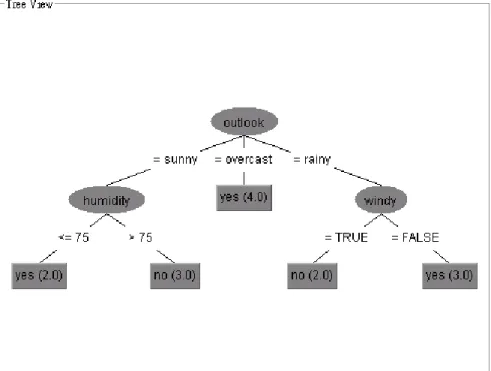
Decision tree is arguably the most widely used approach for classification because it is an effective method for producing classifiers from a dataset. It is also relatively simple, readable and fast to generate. It works by building a tree of rules (see Figure 2.18) whereby new instances can be tested by simply stepping through each test at each decision node starting from the root node till the leaf node. The advantage of this method is that it follows a logical approach and does not make any assumptions on the statistical distribution and independence of features. Thus it is normally more robust compared to most statistical approaches.
The biggest problem for decision tree is the missing branch (null leaf) phenomena. It occurs when the tree is used to classify a feature that is not found in the training set. This will result in an unclassified instance. When building a decision tree, it is important to choose which attributes to split as some choice of attributes may be considerably more useful than others. Basically, the attribute that has the most ‘pure’
nodes and randomly equal counts will be selected. Entropy which is an information theoretic measure of the ‘uncertainty’ contained in a training set, due to the presence of more than one possible classification [8].
28
Figure 2.18 Example of decision tree using WEKA
B. Naive Bayes classifier
NBC is a statistical classifier that predicts the probability that a given combination of features belongs a particular class as shown in Figure 2.19. In certain types of applications, this classifier is found to be comparable to decision trees. It also has the ability to overcome the ‘missing branch’ phenomena because prior and conditional probabilities are both used to calculate the probability of each possible classification.
Theoretically, Bayesian classifiers have the minimum error rate in comparison to all other classifiers. However in practical applications, the statistical assumptions that it imposes will reduce the classification accuracy. Another disadvantage is that it only applies to discrete features, which limits its application. Additionally a complex equation is required for estimating the classification probability and all features must be mutually independent [8].
29
Figure 2.19 The generative process by NBC
C. Bagging on decision tree
Boostrap aggregating (bagging) can improve the performance of decision trees.
It combines multiple rather than using total isolation of classes. Thus a particular set of features can be categorized into several types of classes and their membership into each of the class types is scored. As show in Figure 2.20, the decision rules (base learners) are built different by training them using slightly different training sets. It is then the decision from each decision rules being vote to find the majority. Bagging classifier often gives a higher accuracy than a single classifier because it attempts to neutralize the instability of learning methods by simulating the process described previously using a given training set. This method excels especially when unstable base algorithms with high variance are used. Additionally, it does not tend to over fit the data which makes the final decision less affected by noisy data [8].
Figure 2.20 General framework of bagging
30
D. LogitBoost
Boosting is an ensemble method that is similar in concept to bagging. As shown in Figure 2.21, boosting trains the next weak learners based on the mistakes of previous learners. Normally, boosting results in better performance over bagging.
However, it has a risk of over fitting and thus the performance of combined hypotheses might be worse than the performance of a single hypothesis. Besides, boosting requires a very large training set sample and is unsuitable for small datasets.
Although there are many boosting algorithms available, this research only considered the use of LogitBoost, which performs additive logistic regression. This method can be accelerated by specifying a threshold for weight pruning. The advantage of LogitBoost over other boosting methods is its capability of being wrapped around any numeric predictor without making any modifications. However, it was required to do some regression, and due to the curse of dimension, doing regression is not a trivial task. Thus neutral network was implemented in this project for regression [8].
Figure 2.21 Boosting illustration
31
2.5 The WEKA data mining workbench
WEKA has several graphical user interfaces that enable easy access to the underlying functionality. The main graphical user interface is the “Explorer”. It has a panel-based interface, where different panels correspond to different data mining tasks. In the first panel, called “Preprocess” panel, data can be loaded and transformed using WEKA’s data preprocessing tools, called “filters”. This panel is shown in Figure 2.22.
Figure 2.22 The WEKA explorer interface
The main graphical user interface in WEKA is the “Experimenter” (see Figure 2.23).
This interface is designed to facilitate experimental comparison of the predictive performance of algorithms based on the many different evaluation criteria that are available in WEKA. Experiments can involve multiple algorithms that are run across multiple datasets; for example, using repeated cross-validation. Experiments can also be distributed across different compute nodes in a network to reduce the computational load for individual nodes. All data mining algorithms we introduced previously can be found in WEKA classifier [18, 19].
32
Figure 2.23 The WEKA experimenter interface
Chapter 3 Materials and Methods
3.1 Materials
In this section, we described where to get all the data set of variations characteristic spatial patterns of CP maps representing in Line, Bull eye, Ring, Blob, and Edge. In semiconductor industry, the Engineering Data Analysis System (EDAs) is collecting all measurement data and equipment information in step of process for each device (see Figure 3.1). We obtained hundreds of data from database of EDAs and used as training set. Besides, simulated data was generated and used because the amount of real manufacturing data in EDA database is not sufficient to contain all possible cases. Some patterns rarely occur in real datasets thus they will not provide sufficient coverage when training the classifier. After all, we listed the data set in manufacturing and simulated in Table 3.1.
33
Figure 3.1 The EDA database in semiconductor industry
More precisely, the manufacturing data consist of 758 wafers with 626 dies per wafer and 965 simulated wafers generated by artificiality.
Table 3.1 The EDA database in semiconductor industry
Table 3.x The simulate data set
34
3.2 System flow
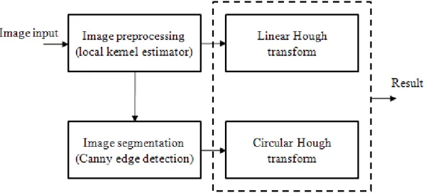
As discussing the related works in Chapter 2, the steps of our methodology are depicted in Figure 3.2. Each step of block will be explained in the following section.
Figure 3.2 System flow
3.3 Methods
3.3.1 Pattern definition
The characteristic pattern is composed of basic shape, mainly including Line, Bull eye, Ring, Blob, and Edge. Because of these patterns can be used to trace back to
the problems that originated the failures either by analyzing their qualitative features or by correlating them with the lot history, so we defined these pattern as our major classified spatial pattern shape as shown in Figure 3.3.
35
Figure 3.3 Pattern definition (a) Line (b) Edge (c) Ring (d) Blob (e) Bull eye
3.3.2 Data preprocessing
In order to eliminate the amount of noise bring from random error, we applied an approach called local kernel estimator which described in section 2.2 to generating smoothed wafer maps. First, the original wafer map must transfer to monochrome image. Second, we generating smoothed image using local kernel estimator, the result resented as gray-level image. Finally we set a threshold value with 0.71 which is optimization by trial and error to filter out random pixels and then obtained a clearly image with system error. The whole procedure is shown in Figure 3.5.
36
Figure 3.5 Filter origin map (a) Original image (b) Monochrome image (c) Gray-level image with (d) Gray-level image with threshold = 0.71
After smoothed the image, an edge recognition procedure is implemented to find all edges in the image. The edge detection process is very important and required procedure for the Circular Hough transform technique. Various edge detection methods have been applied for different application such as Canny., as shown in Figure 3.6.
37
Figure 3.6 The result of an edge recognition procedure in a sample wafer
3.3.3 Feature extraction
In order to prove the Hough transform for lines detection, we involved the real failure of scratch pattern, as shown in Figure 3.7 (a), in semiconductor manufacturing.
Figure 3.7 Line detection of Hough transform (a) Wafer with a scratch signature (b) Filter out random failures (c) Transformed into r-θ parameter space. (d) Frequency histogram of the signature
Afterward, we managed a filter algorithm to filter out the random failures from the original Line spatial pattern and obtained the identified cluster, as shown in Figure 3.7 (b). This procedure can reduce the number of wafers and dies that must be analyzed.
When transformed the signature pattern from image space into the r-θ parameter
38
space, all the dies in the same line are intersected to a point at the angle 135 degree, as shown in Figure 3.7 (c). To automate the classification process, we count the number of die with the identical values of (r ,θ) for the cluster, the result can be visualized as a 2-dimensional frequency histogram, as shown in Figure 3.7 (d). Thus, from the frequency data we automatically identify this pattern as a potential diagonal scratch.
Any other cluster composed of lines, scratches can be identified at the angles of 0, 45, 90 and 135 degrees, as shown in Figure 3.8.
Pattern r-θ parameter space 3D histogram
(a)
(b)
(c)
(d)
Figure 3.8 Four angle line detection of Hough transform (a) 0 degree (b) 45 degree (c) 90 degree (d) 135 degree
In the following, we could notice that the frequency histogram for the cluster composed of ring signature, as shown in Figure 3.9 (a), is not be so characterized and
39
average distributed at the angles of 0, 45, 90 and 135 degrees. This result of frequency histogram caused us to confuse with Bull eye, Ring and Edge signature, as shown in Figure 3.9 (b) (c) (d). This result is presenting that the linear Hough transform is not enough to determine the signature without Line signature pattern. Therefore, we further employed the circular Hough transform method to distinguish the kind of Bull eye and Blob spatial pattern.
Pattern r- θ parameter space 3D histogram
(a)
(b)
(c)
(d)
Figure 3.9 Linear Hough transform for variant shape (a) Bull eye (b) Blob. (c) Ring (d) Edge
The circle is similar to represent in parameter space, compared to the line. As we described in section 2.4.2, each edge point we draw a circle with center in the point with the desired radius, when the edge points in the xy-plane are located on the same
40
perimeter then the circles with center in these points must be intersected to a point, as shown in Figure 3.10 (a). At the coordinates which belong to the perimeter of the drawn circle we increment the value in our accumulator matrix. In this way we sweep over every edge point in the input image drawing circles with the desired radii and incrementing the values (or score) in our accumulator. When every edge point and ever desired radius is used, we can turn our attention to the accumulator, as shown in Figure 3.10 (b). The accumulator matrix which is three dimensional, if the radius is not held constant, can quite fast grow large. In order to simplify the parametric representation of the circle, the radius can be limited to number of known radii, such as 1 < r < R where R is the wafer radius.
(a)
(b)
Figure 3.10 Circle detection using circular Hough transform (a) 4 points are located on the same perimeter with radius r in the xy-plane and 4 circles are intersected to a
41
point (b) Sample of the accumulator matrix
In general, the signatures of Bull eye and Blob spatial pattern on wafers could not be representing in completely circular shape. It could be in elliptic or arbitrary shape.
Thus the maximum score in the accumulator will not be the optimal selection. To find the optimal selection in the accumulator we defined an equation named cover ratio as following:
circle 100 detected in dies total
circle detected in dies failed (%) Ratio
Cover = ´
where the radius of the circle r< (x-a)2+(y-b)2 .
Therefore, based on the accumulator matrix we created previously, finding a set of center (x, y) and radius of circle in the accumulator and calculated the CR. Once the CR has been exceeded the threshold value (for instance, CR=0.9) then we could pick up this set of center and radius for our optimal parameter. The procedure result shown in Figure 3.11.
Index 1 2 3 4
Center of Circle (26, 5) (26, 7) (26, 6) (27, 11)
Radius 13 12 12 8
CR CR = 46.33% CR = 55.71% CR = 51.5% CR = 90.02%
Illustration
Figure 3.11 Finding optimal CR
There is a situation should be noticed that the circle we found by circular Hough transform could be located in small area of failed dies (Figure 3.12). Thus, we must set a criteria to eliminate this situation occur. The criteria set as following:
42
wafer 100 in dies failed Total
circle in dies failed Total (%) Wafer of
Circle = ´
Figure 3.12 Circle detection in Ring and Blob spatial pattern
After we found a set of optimal center and radius, we further distinguish the spatial pattern between Bull eye and Blob by calculated the distance form wafer center to optimal center as shown in Figure 3.13. When the distance is large enough, the spatial pattern could correspond to the characteristic values of Blob spatial pattern.
43
Otherwise, there failure shape could be Bull eye spatial pattern.
Figure 3.13 The distance of Bull eye and Blob spatial pattern
The final portion of the feature extraction divided the wafer map into two zones as show in Figure 10, which zone1 occupied 4/5 of the wafer and zone2 occupied 1/5 of the wafer as shown in Figure 3.14.
Figure 3.14 Wafer splitting
In order to extract the features of ring and edge shapes, we only consider the number of failed dies in zone2, so we defined the Zone Ratio as:
44
zone2 100 in dies total
zone2 in dies failed
(%) Ratio
Zone = ´
For instance, in Figure 11, if the failed pattern represent in ring signature, the calculated values of zone ratio showing a high percentage. If the failed pattern represent in edge signature, the calculated value of zone ratio showing a moderate percentage. Of course, when the failed patterns represent in Blob signature which is very close to the boundary of wafer map, it could also has a moderate percentage values of zone ratio. However, the Blob spatial pattern will be detected by CHT and calculated a distance between detected circle and wafer center, but edge spatial patterns will not. So, it can still effectively identify the edge spatial pattern.
Figure 3.15 Failed ratio in zone
All of the features that we discussed previously can be summarized in Table7. When the linear HT feature has an obvious intersection in a certain angle, we can almost determine the spatial pattern has Line signature. The CHT distance can detect whether there is a circular signature distribution on the wafer and the Zone ratio can detect
45
ring and edge signature similarly.
Table 3.2 Relationship between features and patterns
46
Chapter 4 Results
The methodology must be capable of mapping the features which are extracted from the input to the output. A so-called train and test method is used to construct a classifier in which the available dataset is divided into a training set and a test set, as show in Figure 4.1 [8]. The original data has been divided into training set and testing set. The training set used to train a classified model by data mining classification algorithm with 10-folds cross-validation. Once the classified model had been constructed, the testing set will applied to estimate the accuracy of classifier.
Figure 4.1 System interface I (a) Load the original EWS map in the system (b) Filter out random failed dies
4.1 Implementation
As the experiment we have shown previously, and then we developed an automatic recognition application to implement our serial procedure of classification.
The automatic recognition system is implemented using Visual Studio C# language under Microsoft Windows XP operation system. In this section, the automatic recognition system will be introduced.
47
1. Load the original CP map in the system and filter out random failed dies.
2. Hough transform for linear detection.
Figure 4.2 System interface I (a) Load the original EWS map and filter out random failed dies (b) Hough transform for linear detection
3. Edge detection.
4. Hough transform for circular detection.
Figure 4.3 System interface II (a) Edge detection (b) Hough transform for circular detection
(a) (b)
(a) (b)
![Figure 2.3 Wafer level testing [22]](https://thumb-ap.123doks.com/thumbv2/9libinfo/9501442.595984/16.893.239.661.790.1041/figure-wafer-level-testing.webp)