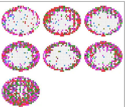
Development Pattern Recognition Model for Classification of Circuit Probe Wafer Maps on Semiconductors
全文
數據
![Figure 2.3 Wafer level testing [22]](https://thumb-ap.123doks.com/thumbv2/9libinfo/9501442.595984/16.893.239.661.790.1041/figure-wafer-level-testing.webp)
Outline
相關文件
2 Center for Theoretical Sciences and Center for Quantum Science and Engineering, National Taiwan University, Taipei 10617, Taiwan!. ⇤ Author to whom correspondence should
If the best number of degrees of freedom for pure error can be specified, we might use some standard optimality criterion to obtain an optimal design for the given model, and
Mathematical theories explain the relations among patterns; functions and maps, operators and morphisms bind one type of pattern to another to yield lasting
Retrieval performance of different texture features according to the number of relevant images retrieved at various scopes using Corel Photo galleries. # of top
Advantages of linear: easier feature engineering We expect that linear classification can be widely used in situations ranging from small-model to big-data classification. Chih-Jen
Tekalp, “Frontal-View Face Detection and Facial Feature Extraction Using Color, Shape and Symmetry Based Cost Functions,” Pattern Recognition Letters, vol.. Fujibayashi,
Proceedings of IEEE Conference on Computer Vision and Pattern Recognition, pp... Annealed
(2) We emphasized that our method uses compressed video data to train and detect human behavior, while the proposed method of [19] Alireza Fathi and Greg Mori can only
