國立臺灣大學高分子科學與工程學研究所 碩士論文
Institute of Polymer Science and Engineering College of Engineering
National Taiwan University Master Thesis
新型含三苯胺結構之高性能高分子合成與 記憶體元件應用之研究
Synthesis and Memory Device Applications of Novel Triphenylamine Moiety Based
High-Performance Polymers
胡益誠 Yi-Cheng Hu
指導教授:劉貴生 博士 Advisor: Guey-Sheng Liou, Ph. D.
中華民國 101 年 8 月 Aug., 2012
i
ii
ACKNOWLEDGEMENTS
I feel an immense gratitude to my advisor, Prof. Guey-Sheng Liou, for everything in this two year. In addition, I appreciate Prof. Sheng-Huei Hsiao, Assistant Prof.
Shih-Huang Tung, and Prof. Chao-Sung Lai for their perceptive criticisms and useful comments on this dissertation and all teachers at Institute of Polymer Science and Engineering in the National Taiwan University. A financial supports from the National Science Council of the Republic of China and a congenial environment for my graduate studies provided by the Institute of Polymer Science and Engineering at the National Taiwan University are also greatly appreciated.
I appreciate Associate Prof. Sheng-Shu Hou and all the teachers in Dept. of Chemical Engineering, National Cheng Kung University for the tuitions and the partners of studying group for graduate school entrance exams in the K-House; all of you gave me the opportunity of taking my master degree here.
I also appreciate Hung-Ju Yen for his advice and suggestion at key times, princess Chen for her humor and aid, Wan-Jiun Wu for being together with me and her thoughtfulness, Feng-Jeng Lin for the assistance in photographing TEM images, and the fellows in G. S. Liou’s Lab. : Chia-Liang Tsai, Jia-Hao Wu, Pei-Hsuan Wang, Kun-Ying Lin, Shiue-Ming Kuo, Zheng-Wei Liu, Chih-Lung Heish, Lin-En Chi, Wen-Chang Wang, Wei-Yao Tung, Ya-Wen Chuang, Shih-Han Chen, Jhe-Huang Lin. I can not finish this thesis without their supports and encouragement.
I would like to show my appreciation to the members in baseball teams of KSHS, NCKUCHE, NCKU, NTU, and YS confidence baseball club, for all of you delight my life.
Finally, I am grateful to my family for their endless love and supports, especially to my mother who makes me never blind even facing adversities or prosperities. I would like to dedicate all my achievements to them.
iii
ABSTRACT
This study has been separated into five chapters. Chapter 1 is general introduction.
Chapter 2 includes two distinct approaches to synthesize the active layer in the application of memory devices. The first one is introducing PCBM as the acceptor via blending into the donor-containing poly-4-methoxytriphenylamine (P-TPA) leading the donor-acceptor hybrid films P-TPA:PCBM, another one is incorporating the acceptor anthraquinone via covalent bond to the electron-donating moiety then
resulting donor-acceptor containing polymers
poly-2-diphenylaminoanthracene-9,10-dione (P-TPAAQ) and poly-2-(4-diphenylaminophenoxy)anthracene-9,10-dione (P-TPAOAQ). Chapter 3 describes the memory devices based on dual competitive electron acceptors system with novel electron-donating triphenylamine (TPA) based electroactive functional polyimides AQ-PIs and OAQ-PIs derived from two diamines,
2-(bis(4-aminophenyl)amino)anthracene-9,10-dione and
2-(4-(bis(4-aminophenyl)amino)phenoxy)anthracene-9,10-dione, respectively, having electron-withdrawing pendent anthraquinone moiety. Chapter 4 describes the structurally related TPA-based polyimides (PIs), polyamides (PAs), and polyethers (PEs) with different donor-linkage-acceptor (D-L-A) units for the systematical study and comparison of both linkage and acceptor effects on the memory behaviors. The synthesis and basic characterization of the obtained aromatic TPA-based polymers were described. Chapter 5 contains conclusions. Besides, the memory characteristics were investigated by I-V measurements and compared. The corresponding morphology study, optical characteristic, electrochemical and spectroelectrochemical properties, and theoretical analysis results were used to demonstrate that the resulting memory behaviors could be elucidated by the charge-transfer mechanism.
Keyword: triphenylamine, memory, highperformance polymers, donor, acceptor,
iv
charge transfer mechanism.
v
中文摘要
本論文分成五個章節,第一章為總體序論。第二章描述了兩種合成作為記憶體 主動層材料的方法。第一種為將電子受體藉由混摻的方式導入含電子施體的高分 子 poly-4-methoxytriphenylamine (P-TPA) 而 得 具 電 子 施 體 與 受 體 的 複 合 材 料:P-TPA:PCBM。 另一種為將可作為電子受體的蒽醌基團藉由化學共價鍵的 方 式 導 入 含 電 子 施 體 的 結 構 再 進 而 聚 合 而 得 具 電 子 施 體 與 受 體 的 高 分 子
poly-2-diphenylaminoanthracene-9,10-dione (P-TPAAQ) 與
poly-2-(4-diphenylaminophenoxy)anthracene-9,10-dione (P-TPAOAQ)。第三章係探
討 分 別 以 具 電 活 性 的 二 胺 化 合 物
2-(bis(4-aminophenyl)amino)anthracene-9,10-dione 與
2-(4-(bis(4-aminophenyl)amino)phenoxy)anthracene-9,10-dione 所合成之含電子施 體三苯胺與側鏈上具拉電子能力的蒽醌取代基而得具兩個相互競爭的電子受體 基團的新穎性聚醯亞胺 AQ-PIs 與 OAQ-PIs 所製得之記憶體元件。第四章係以 三苯胺作為電子施體的聚醯亞胺(PIs)與類似結構但含不同連接基團與電子受體 的聚醯胺(PAs)與聚醚 (PEs)於連接基團與電子受體對於記憶體性質的影響做 一有系統的研究與比較。第五章節為結論。上述含三苯胺之芳香族高分子的合 成、基本特性皆被研究。此外,所有的記憶體性質皆由其 I-V 的特性來進行探討。
並由相關的表面型態分析、光學性質、電化學及光譜電化學分析及理論計算可推 論本研究中所得的記憶體性質可由電荷轉移(charge-transfer)機制解釋。
關鍵字: 三苯胺、記憶體、高性能高分子、電子施體、電子受體、電荷轉移機 制
vi
TABLE OF CONTENTS
ACKNOWLEDGEMTS ... ii
ABSTRACT (in English) ... iii
ABSTRACT (in Chinese) ... v
TABLE OF CONTENTS ... vi
LIST OF TABLES ... xii
LIST OF FIGURES ... xiii
CHAPTER 1 ... 1
CHAPTER 2 ... 36
CHAPTER 3 ... 75
CHAPTER 4 ... 108
CHAPTER 5 ... 140
APPENDIX ... 143
vii
CHAPTER 1
General Introduction
1.1 HIGH PERFORMANCE POLYMERS ... 2
1.1.1 Preparation of Aromatic Polyamides ... 4
1.1.2 High-temperature Solution Methods ... 5
1.1.3 Low-temperature Solution Methods ... 6
1.1.4 Preparation of Aromatic Polyimides ... 7
1.2 Introduction to Polymer Memory ...10
1.2.1 General Concepts ... 10
1.2.2 Fundamentals and Device Architecture of Resistor-type Polymeric Memory 11 1.3 Mechanisms of Polymer Memory ...14
1.3.1 Filamentary Mechanism ... 14
1.3.2 Trapping-Detrapping Mechanism ... 15
1.3.3 Charge Transfer Mechanism... 18
1.4 Evolution of Polymer Memory ...21
1.4.1 Polymer Composites ... 21
1.4.2 Conjugated Polymers ... 22
1.4.3 Non-conjugated Polymers With Specific Pendent Groups ... 24
1.4.4 Functional High Performance Polymers ... 26
1.5 Research Motivations ...28
REFERENCES AND NOTES ...31
viii
CHAPTER 2
Electrically Bistable Memory devices Derived from Poly(triphenylamine)s Derivatives and its PCBM Hybrid Films
ABSTRACT OF CHAPTER 2 ...37
2.1 INTRODUCTION ...38
2.2 EXPERIMENTAL SECTION ...41
2.2.1 Materials ... 41
2.2.2 Monomer Synthesis ... 41
2.2.3 Polymer Synthesis ... 43
2.2.4 Measurements ... 44
2.2.5 Fabrication and Measurement of the Memory Device ... 45
2.2.6 Theoretical Calculation ... 45
2.3 RESULTS AND DISCUSSION...47
2.3.1 Monomer Synthesis ... 47
2.3.2 Polymer Synthesis ... 50
2.3.3 Basic Characteristic Polymer Properties ... 51
2.3.4 Electrochemical Properties ... 54
2.3.5 Memory Device Characteristics of the P-TPA:PCBM Hybrid films ... 59
2.3.6 Memory Device Characteristics of the P-TPAAQ and P-TPAOAQ ... 62
2.3.7 Switching Mechanism of the P-TPA:PCBM, P-TPAAQ, and P-TPAOAQ 65 2.4 SUMMARY ... 70
REFERENCES AND NOTES ...71
ix
CHAPTER 3
Memory Behaviors Resulted From Functional Polyimide Systems Containing Triphenylamine With Dual Competitive Electron Acceptors
ABSTRACT OF CHAPTER 3 ...76
3.1 INTRODUCTION ...77
3.2 EXPERIMENTAL SECTION ...80
3.2.1 Materials ... 80
3.2.2 Polymer Synthesis ... 80
3.2.3 Measurements ... 83
3.2.4 Fabrication and Measurement of the Memory Device ... 83
3.2.5 Molecular Simulation ... 84
3.3 RESULTS AND DISCUSSION...85
3.3.1 Polymer Synthesis ... 85
3.3.2 Electrochemical Properties ... 86
3.3.3 Memory Device Characteristics of the AQ-PIs and OAQ-PIs... 91
3.3.4 Switching Mechanism of the AQ-PIs and OAQ-PIs ... 96
3.3.5 Spectroelectrochemistry ...100
3.4 SUMMARY ... 104
REFERENCES AND NOTES ... 105
x
CHAPTER 4
High Performance Polymers With Different D-L-A Containing
for Memory Application
ABSTRACT OF CHAPTER 4 ... 109
4.1 INTRODUCTION ... 110
4.2 EXPERIMENTAL SECTION ... 112
4.2.1 Materials ...112
4.2.2 Polymer Synthesis ...112
4.2.3 Measurements ...113
4.2.4 Fabrication and Measurement of the Memory Device ...114
4.2.5 Theoretical Calculation ...115
4.3 RESULTS AND DISCUSSION... 116
4.3.1 Polymer Synthesis ...116
4.3.2 Thermal Properties and Solubility Behavior of the Polymers ...118
4.3.3 Optical and Electrochemical Properties ...122
4.3.4 Switching Behaviors of These Polymeric Memory Devices ...126
4.3.5 Theoretical Analysis and Switching Mechanism ...130
4.4 SUMMARY ... 134
REFERENCES AND NOTES ... 135
xi
CHAPTER 5
CONCLUSIONS
CONCLUSIONS ... 109
xii
LIST OF TABLES
CHAPTER 1
Table 1.1. Some Typical Aromatic High Performance Polymers ………3
Table 1.2. Commercially Available Aromatic Polyamides…………...………6
Table 1.3. Commercially Available Aromatic Polyimides ………...………9
CHAPTER 2 Table 2.1. Inherent Viscosity and Molecular Weights of Studied Materials ……..…52
Table 2.2. Thermal Properties of Obtained Polymers….……….………...…52
Table 2.3. Redox Potentials and Energy Levels of Studying Polymers ……….56
CHAPTER 3 Table 3.1. Inherent Viscosity and Molecular Weights of Polyimides ………85
Table 3.2. Redox Potentials and Energy Levels of Polyimides .……….88
CHAPTER 4 Table 4.1. Inherent Viscosity and Molecular Weights of Polymers ………...117
Table 4.2. Thermal Properties of Obtained Polymers ...………...120
Table 4.3. Solubility Behavior of Prepared Polymers ………...120
Table 4.4. Redox Potentials and Energy Levels of Polymers ………...123
xiii
LIST OF FIGURES
CHAPTER 1
Figure 1.1. Classification of electronic memories...………11 Figure 1.2. Architecture of MIM sandwich polymer memory device………...……..11 Figure 1.3. Some evaluation parameters for molecular/polymer memories. (a)
Stability under voltage stress and ON/OFF ratio (inset); (b) Number of read pulses; (c) Write–read–erase–read (WRER) cycles; (d) Switching time measurement. ... 13 Figure 1.4. Schematic illustration of the formation of (a) carbon-rich filaments and (b) metallic filaments, and the relevant switching effects... 15 Figure 1.5. (a) Operational mechanism of the memory. Experimental and fitted J–V curves of the ITO/PFOxPy/Al device (b) OFF state with the Ohmic current (<1.3 V) and SCLC (1.3–2.6 V) models, (c) ON state with the Ohmic current model (>2.8 V).
... 17 Figure 1.6. (a) I–V (in log scale) curves of the Al/Au:NP/Al bistable memory device.
(b) Schematic band diagrams for the transport mechanism of trap-filled SCLC: (i) Region I: thermally generated carrier conduction, (ii) Region II: with traps, (iii)
Region III: nearly filled, and (iv) Region IV: traps filled. ... 18 Figure 1.7. Schematic representation of the formation of ion-radical species and charge transfer complexes. ... 20 Figure 1.8. Molecular orbitals (left) of the basic unit of TP6F–PI and the transitions (right) from the ground state to the charge transfer state induced by the electric field.
... 20 Figure 1.9. Molecular structures of donor–acceptor polymer systems for advanced memory device applications.57 ... 21
xiv
Figure 1.10. Memory devices based on poly(triphenylamine)s derivatives and its
PCBM hybrid film. ... 29
Figure 1.11. Memory devices fabricated by functional polyimide containing TPA with dual competitive electron acceptors. ... 29
Figure 1.12. The approaching way for discussing the linkage group effect on their memory characteristic in corresponding D-L-A containing polymers of PIs, PAs, and PEs, and the schematic diagram of the memory device consisting of a polymer thin film sandwiched between an ITO bottom electrode and an Al top electrode. ... 30
CHAPTER 2 Figure 2.1. The schematic diagram of the memory device consisting of a polymeric active layer sandwiched between an ITO bottom electrode and an Al top electrode. The thickness of polymeric thin film is about 50 nm and the thickness of electrode is 300nm. ... 46
Figure 2.2. IR spectra of (a) compound 3 and (b) compound 4. ... 48
Figure 2.3. 1H NMR spectra of compound 3 in DMSO-d6. ... 49
Figure 2.4. 1H NMR spectra of compound 4 in DMSO-d6. ... 49
Figure 2.5. TGA thermograms of P-TPA, P-TPAAQ, and P-TPAOAQ at a scan rate of 20 oC/min. ... 53
Figure 2.6. Cyclic voltammetric diagrams of P-TPA films on an ITO-coated glass substrate over cyclic scans in 0.1 M TBAP/CH3CN at a scan rate of 100 mV/s. ... 56
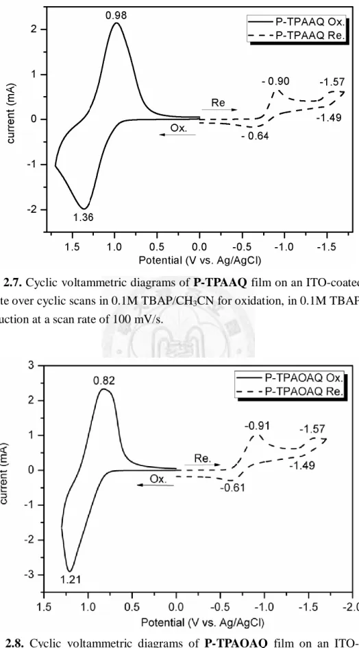
Figure 2.7. Cyclic voltammetric diagrams of P-TPAAQ film on an ITO-coated glass substrate over cyclic scans in 0.1M TBAP/CH3CN for oxidation, in 0.1M TBAP/DMF for reduction at a scan rate of 100 mV/s.. ... 57 Figure 2.8. Cyclic voltammetric diagrams of P-TPAOAQ film on an ITO-coated
xv
glass substrate over cyclic scans in 0.1M TBAP/CH3CN for oxidation, in 0.1M
TBAP/DMF for reduction at a scan rate of 100 mV/s... 57 Figure 2.9. Continuous cyclic voltammetric diagrams of (a) P-TPAAQ and (b)
P-TPAOAQ films on an ITO-coated glass substrate over cyclic scans in 0.1 M
TBAP/CH3CN at a scan rate of 100 mV/s. ... 58 Figure 2.10. Current-voltage (I-V) characteristics of the ITO/P-TPA:PCBM/Al memory device with (a) 0%, (b) 1%, (c) 3%, (d) 5%, (e) 4%, (f) 4%, and (g) 10%
PCBM weight fraction. ... 61 Figure 2.11. Current-voltage (I-V) characteristics of the (a) ITO/P-TPAAQ/Al, and (b) ITO/P-TPAOAQ/Al memory device. The time interval between the third and fourth sweep is 20 seconds and 6 minutes, respectively... 64 Figure 2.12. Photoluminescence spectra of P-TPA:PCBM hybrid thin films. ... 68 Figure 2.13. The TEM images of (a) 3 wt%, (b) 4 wt%, and (c) 5 wt% P-TPA:PCBM spin-coating films. ... 68 Figure 2.14. Calculated molecular orbitals and corresponding energy levels of the basic units (BU) for P-TPAAQ (left) and P-TPAOAQ (right). ... 69
CHAPTER 3
Figure 3.1. IR spectrum of polyimide AQ-6FPI film. ... 82 Figure 3.2. Molecular structure of AQ-PIs and OAQ-PIs and schematic diagram of the memory device consisting of a polymer thin film sandwiched between an ITO bottom electrode and an Al top electrode. The thickness of polymer film is about 50 nm and the thickness of electrode is 300nm. ... 84 Figure 3.3. Cyclic voltammetric diagrams of polyimide (a) AQ-6FPI and (b)
OAQ-6FPI films on an ITO-coated glass substrate over cyclic scans in 0.1M
xvi
TBAP/DMF at a scan rate of 50 mV/s. ... 89 Figure 3.4. Cyclic voltammetric diagrams of polyimide (a) AQ-DSPI and (b)
OAQ-DSPI films on an ITO-coated glass substrate over cyclic scans in 0.1M
TBAP/DMF at a scan rate of 50 mV/s. ... 90 Figure 3.5. (a) Current-voltage (I-V) characteristics of the ITO/AQ-6FPI/Al memory device (The time interval between the first and second sweep is less than 5 seconds), (b) Current-voltage (I-V) characteristics of the ITO/OAQ-6FPI/Al memory device (The time interval between the third and fourth sweep is 8 minutes). ... 93 Figure 3.6. (a) Dual sweep current-voltage (I-V) characteristics of the
ITO/AQ-6FPI/Al memory device. Each dual sweep process will turn to off state during the backward sweep. (b) Effect of operation time on the ON and OFF states of the ITO/OAQ-6FPI/Al device with a continue -2 V. ... 94 Figure 3.7. (a) Current-voltage (I-V) characteristics of the ITO/AQ-DSPI/Al memory device and (b) Current-voltage (I-V) characteristics of the ITO/OAQ-DSPI/Al
memory device. The time interval between the third and fourth sweep is 10 and 8 minutes, respectively. ... 95 Figure 3.8. Calculated molecular orbitals and corresponding energy levels of the basic units (BU) for OAQ-6PFI and AQ-6FPI. ... 98 Figure 3.9. Calculated molecular orbitals and corresponding energy levels of the basic units (BU) for OAQ-DSPI and AQ-DSPI. ... 99 Figure 3.10. UV-vis-NIR spectra of polyimide (a) OAQ-6FPI (b) TPA-6FPI thin film on the ITO-coated glass substrate in 0.1 M TBAP/DMF. ...102 Figure 3.11. UV-vis-NIR spectra of polyimide OAQ-DSPI thin film on the
ITO-coated glass substrate in 0.1 M TBAP/DMF. ...103
xvii
CHAPTER 4
Figure 4.1. Molecular structure of PIs, PAs and PEs, and schematic diagram of the memory device consisting of a polymer thin film sandwiched between an ITO bottom electrode and an Al top electrode. The thickness of polymer film is about 50 nm and the thickness of electrode is 300nm. ... 115 Figure 4.2. IR spectra of (a) PMPI, and (b) OXPE. ... 118 Figure 4.3. TGA thermograms of PMPI, DSPE, and OXPE at a scan rate of 20
oC/min. ...121 Figure 4.4. TMA curves of PMPI, and DSC traces of DSPE and OXPE. ...121 Figure 4.5. UV-visable absorption spectra of (a) PIs, (b) PAs, and (c) PEs. ...124 Figure 4.6. Cyclic voltammograms of PIs, PAs, and PEs films on an ITO-coated glass substrate in CH3CN containing 0.1 M TBAP at the scan rate of 50 mV/s. ...125 Figure 4.7. Current-voltage (I-V) characteristics of (a) ODPI, (b) 6FPI, (c) DSPI, and (d) ODPI. ………129 Figure 4.8. Current-voltage (I-V) characteristics of (a) ODPA, (b) 6FPA, (c) DSPA, and (d) TPPA. ...129 Figure 4.9. Current-voltage (I-V) characteristics of (a) DSPE, and (b) OXPE. ...129 Figure 4.10. Calculated molecular orbitals and corresponding energy levels of the basic units (BU) for TPA-based PIs. ...132 Figure 4.11. Calculated molecular orbitals and corresponding energy levels of the basic units (BU) for TPA-based PAs. ...133 Figure 4.12. Calculated molecular orbitals and corresponding energy levels of the basic units (BU) for TPA-based PEs. ...133
1
CHAPTER 1
General Introduction
2
1.1 HIGH PERFORMANCE POLYMERS
In nowadays world, polymers are indispensable to our life. Polymers have been widely researched in the 21st century. In particular, high-performance polymers attract lots of attention due to its high thermal stability and good chemical resistance and well mechanical strength which could be modified by introducing different functional groups into the molecular structure. The quest for high-performance polymers began in the late 1950s to meet the demands for military, aerospace, machine-building, electronics, and many industrial applications. Since then, a lot of novel high-performance polymers have been prepared for certain applications. Hill and Walker first found that the incorporation of aromatic segments into a polymer generally results in a tremendous increase in its thermal stability.1 From this viewpoint, much of the research work has been directed toward aromatic compositions. As the result, high-performance polymers usually tend to contain more aromatic units within structure. Several of these aromatic high-performance polymers have reached commercialization such as aromatic polyamides, polyimides, polyesters, polysulfones, and heterocyclic polymers (Table 1.1). Aromatic polyamides (aramids) and polyimides, such as DuPont’s Kevlar fiber and Kapton film, have been well known for a long time and constantly draw much interest more than other high-performance polymers for their several practical properties such as excellent thermal and oxidative stability, high mechanical strength, low flammability, good chemical and radiation resistance, and low dielectric constant (for polyimide).2-9
3
Table 1.1. Some Typical Aromatic High Performance Polymers
Polymer Tg (℃) Tm (℃)
Aromatic polyamide
N N C C
Kevlar
H O
H O
n
-a -
N N C C
Nomex
H
H O O
n
272 435
Aromatic polyimide
N N O
O
O
O
O n
Kapton
399 -
Upilex R N
O
O
N O
O
O n
303 -
Aromatic polyester
188 -
Aromatic polysulfone
PST S O C
CH3 CH3
O O
O n
189 -
Aromatic heterocyclic polymer
PBT
N
S N
S
n
- -
a Not detected
4
1.1.1 Preparation of Aromatic Polyamides10
The properties of aromatic polyamides (aramids) are quite different from those of the aliphatic polyamides (nylons), for instance, thermal resistance and low flammability. In general, they have high melting points above 300 oC and in many cases higher than 350 oC. Some of the commercial available aromatic polyamides are collected in Table 1.2. Nomex and Kevlar aramid fibers which were synthesized and commercialized by DuPont are the most well-known. It is renowned for its high thermal stability and typically used to fabricate fire protective textile in early time. In nowadays, it is used as the high modulus and high strength fiber for bulletproof vests, radial tires, ropes, thermal insulating clothing, and advanced composites. Nomex aramid was prepared by DuPont in 1961 as first commercial high-temperature synthetic fiber. It is based on poly(m-phenyleneisophthalamide), which contains meta-oriented chain segments of the AA-BB configuration. Subsequently, Kevlar aramid was synthesized and commercialized by DuPont in 1972. It is based on poly(p-phenyleneterephthalamide), one of the para-oriented aromatic polyamides synthesized by S.L. Kwolek ( a researcher of DuPont ). Kevlar aramid can be prepared in some synthesis routes. The classical procedure contains the low temperature polycondensation of p-phenylene diamine and terephthaloyl chloride in an amide solvent such as N-methyl-2-pyrrolidone (NMP) with the presence of metal salts like lithium chloride. Kevlar aramid, just like other para-oriented aromatic polyamides, is insoluble in conventional solvents except for strong acids such as concentrated sulfuric acid. The most efficient processes for the preparation of aromatic polyamides illustrated in the following pages are concluding the reaction of diacid dichlorides with diamines at low temperature and direct condensation reactions in solution of aromatic diacids with diamines at high temperatures.
5
1.1.2 High-temperature Solution Methods
In 1971, Ogata11 reported a superior synthesis route for aromatic polyamides by the direct polycondensation of aromatic diamines with aromatic dicarboxylic acids in the presence of an aryl phosphite and an organic base. In the original publication of this novel synthesis for the preparation of polyamides first reported by Ogata was referred to as a phosphorylation reaction,12 resulted the low-molecular-weight polymer . Two significant modifications, presented by Yamazaki, were developed by using triphenyl phosphite (TPP) and pyridine as condensing agents13 and addition of LiCl to the solvent14 for the reaction and led to a considerable increase in the molecular weight of the produced polymers by promoting the solubility (as shown in scheme 1.1). In order to make further progress from that time, many approaches have been developed to optimize the reaction conditions for increasing the molecular weight of polyamides.
For example, Preston and Hofferbert15 reported that the polymerization temperature was raised from 80 to 100 oC, and the higher temperature was subsequently suitable for the synthesis of various polyamides. In 1982, Higashi et al.16 demonstrated that poly(p-phenylene terephthalamide) (Kevlar) with inherent viscosity of 4.5 dL/g could be received by using a solvent medium with presence of both LiCl and CaCl2. Krigbaum and coworkers17-19 have referred to these as Higashi conditions in a series of studies, and they claimed that20,21 the inherent viscosity of Kevlar using Higashi conditions could be enhanced to of 6.2 dL/g via increasing the reaction temperature from 100 to 115 oC. In general, the direct polycondensation could be carried out by high-temperature heating method, adding TPP as the condensation promoter, thus diminishing the reaction times from hours to minutes. It is the most famous and facile procedure for preparing high-molecular-weight aromatic polyamides.
6
Scheme 1.1 Direct polycondensation.
Table 1.2. Commercially Available Aromatic Polyamides
Polymer Tg (oC) Tm (oC)
N N C C
Kevlar
H O
H O
n
- -a
N C
O H
PBA
n
- -
N H3C
N C C
H O O
H
n
KM-21 - -
N N C C
Nomex
H
H O O
n
272 435
N N C C
MeMPD-I
H
H O O
n CH3
260 405
a Not detected.
1.1.3 Low-temperature Solution Methods22
The low temperature solution method has priority when the diacid chloride can be easily obtained from the corresponding aromatic diacid. For example, Kavlar was prepared in NMP by p-phenylenediamine (PPD) and terephthaloyl dichloride (TPC) with some solubility prompters (CaCl2) (as shown in scheme 1.2). The major
7
disadvantage of this way is the monomer with high purity is necessary for getting high molecular weight of polyamide.23
NH2
H2N + C C
O Cl O
Cl
-2n HCl
C C
O H N
O H
N n
Scheme 1.2 1.1.4 Preparation of Aromatic Polyimides
Aromatic polyimides can be regarded as an indispensable materials because of their many excellent characteristics and often replace glass and metals in many industrial usages, especially in the semiconductor and electric packaging industry. The outstanding properties of aromatic polyimides result from their rigid backbones and strong intramolecular and intermolecular interactions between the polymer chains due to the charge transfer complex formation between electron-abounding (diamine moiety) and electron-lacking (dianhydride moiety) segments. Some of the commercial available aromatic polyimides are summarized in Table 1.3. In 1956, Endrey, a researcher of DuPont, received the assignment for seeking an aromatic polyimide film prepared via a soluble intermediate polymeric precursor. He successfully evaluated several solvents that dimethyl formamide (DMF) was an excellent solvent and synthesized the first poly(amic acid) film and demonstrated thermal conversion to polyimide film based on oxydianiline-pyromellitic dianhydride (ODA-PMDA). In 1965, the first commercial aromatic polyimide film was synthesized and named as Kapton, widely used in a lot of applications such as substrate for flexible printed circuit and insulation for transformer and capacitor. In addition, other significant aromatic polyimides have been prepared such as the Upilex series derived from biphenyl dianhydride (BPDA) invented by Ube industries. LARC-TPI is a thermoplastic polyimide developed by NASA Langley Research Center, primarily as a high temperature adhesive. Occidental Chemical Co. pioneered the synthesis of
8
oxydiphthalic dianhydride (ODPA) and defined the properties of ODPA-based polyimides. Aromatic polyimides can be prepared from a variety of starting materials, by a variety of synthetic routes. The typical synthetic methods are shown as the following. Polymerization of diamines and dianhydrides in the classic two-stage method of polyimides synthesis, an aromatic tetracarboxylic dianhydride is added to a solution of aromatic diamine in a polar aprotic solvent. The generated soluble poly(amic acid) can be fabricated into shaped products, and then cyclodehydrated to the corresponding polyimide by extended heating at elevated temperatures (thermal imidization) or by treatment with chemical dehydrating agents (chemical imidization) (as shown in scheme 1.3).24-27 In addition, a simple one-step preparation method of soluble polyimides with high molecular weight was accomplished by heating to 200
oC in m-cresol.28
O Ar' O
Ar NH2 H2N
O
O O
O
N C H O
HOOC
COOH
C N O H Ar'
n
N Ar' N
O
O O
O
Ar n
Ar
Scheme 1.3 Two-step method of polyimides synthesis.
9
Table 1.3. Commercially Available Aromatic Polyimides
Polymer Tg (oC) Tm (oC)
399 -a
264 -
273 -
217 -
a Not detected.
10
1.2 Introduction to Polymer Memory 1.2.1 General Concepts
In the field of Information of Technology (IT), the memory is usually defined as a storage device or recording medium that retains retrievable digital data over a time interval. An electronic memory is fast in response and compact in size, and can be read and written when connected to a central processing unit. This feature distinguishes the electronic memory from other forms of storage, such as CD, DVD, ZIP disk, floppy disk, hard disk and video/audio tape. Differ from conventional memory, which were depended on semiconductor-based integrated circuits, new polymeric materials contains electrical bistability resulting from certain intrinsic properties, such as polarity, magnetism, conformation or especially conductivity, in response to the applied electric field.29
Electronic memories can be divided into two primary classifications by its volatility:
volatile and non-volatile memories. Volatile type loses the stored data as soon as the system is turned off. It needs a constant power supply to keep the stored information.
However, non-volatile type can retain the stored information even when the electrical power supply has been removed. They can be further divided into sub-categories, as shown in Figure 1.1, with the write-once read-many times (WORM) memory, the non-volatile and rewritable (flash) memory. The different between them is that WORM type can remain data permanently and not allow to erase data once it has written, and it works as CD-R, DVD±R. Another flash type memory stored state can be electrically reprogrammed and it has the ability to write, read, erase and retain the stored data, and it have been used in many portable electronic systems, such as mobile computer, PDA, cell-phone and digital camera etc. On the contrary, volatile type includes the dynamic random access memory (DRAM) and the static random access
11
memory (SRAM). DRAM exhibits ability to write, read, erase and refresh the electric states. The SRAM possess longer storage time after removing the electrical field.30-32 Nowadays, DRAM is used as main memory of most computers.
Figure 1.1. Classification of electronic memories.
1.2.2 Fundamentals and Device Architecture of Resistor-type Polymeric Memory Polymer is regarded as promising candidate for memory application for the advantages of the low cost solution process ability and the capability for fabricating three-dimensional device. Instead of the more elaborated process of vacuum evaporation and deposition of inorganic and organic molecule component, solution processes such as spin-coating, dip-coating, roller-coating and ink-jet printing can be used to deposit polymer on kinds of substrates in facile.33 In the typical device, polymer thin film is used as the storage medium and sandwiched between two electrode as metal-insulator-metal (MIM) structure, as shown in Figure 1.2.
I-V
Al
ITO glass 50 nm polymer thin film
0.5 × 0.5 mm2
Figure 1.2. Architecture of MIM sandwich polymer memory device.
12
Devices including switchable resistive materials are generically classified as resistor-type memory, or resistive random access memory (RRAM). It’s different from the conventional memory technologies with the memory effects associated with a especial cell structure (e.g. FET), resistance change memory stores data in an entirely different form. For example, data is stored based on the electrical bistability (ON and OFF states) of materials resulting from changes in certain intrinsic properties, such as charge transfer, phase change, conformation change and reduction–oxidation (redox), in response to the applied electric field as low conductive state and high conductive state and then can be defined as “0” or “1” for digital memory application.29
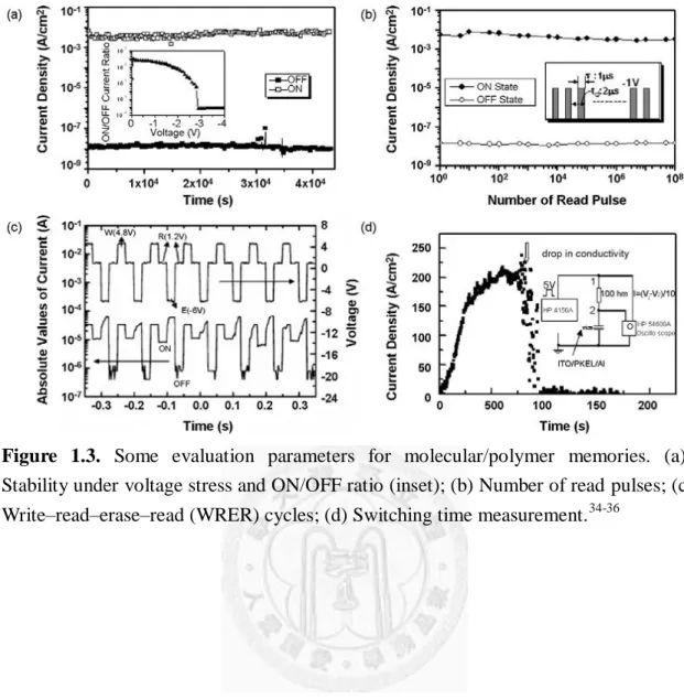
When discussing about polymeric memory devices, some basic parameters of importance to the performance of polymer RRAM device include: (i) ON/OFF current ratio (a higher value is essential for the device to function with minimal misreading error), (ii) switching (write and erase) time, (iii) read time, (iv) retention ability for non-volatile RRAM, (v) programming (or WRER) cycles and long-term stability, (vi) stability under electrical field stress and under read pulses. Examples of evaluation results for some of these parameters are shown in Figure 1.3. Unlike those capacitor-type and transistor-type polymer memories, which still need to be integrated to basic CMOS logic circuits,34 the RRAMs are not based on silicon CMOS technology.
13
Figure 1.3. Some evaluation parameters for molecular/polymer memories. (a) Stability under voltage stress and ON/OFF ratio (inset); (b) Number of read pulses; (c) Write–read–erase–read (WRER) cycles; (d) Switching time measurement.34-36
14
1.3 Mechanisms of Polymer Memory
RRAMs are based on conductivity of the active layer change in response to the applied electric field. The electrical conduction mechanism in polymers is much more complex than in ordered inorganic materials. It cannot be appropriately explained by the basis of band theory, due to most polymers are amorphous in nature.37 As the result, the conduction in polymers is normally explained by (i) intrinsic charge carrier generation and (ii) charge carrier injection from contacts at high fields. The density of intrinsic carriers in polymers except for doped conducting polymers is usually low and the carriers are usually trapped by localized states at room temperature. The local field may promote the detrapping process thus abruptly enhance the conductivity of the polymer thin film.37
1.3.1 Filamentary Mechanism
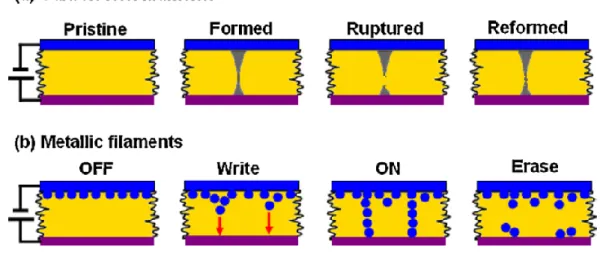
In general, the ON state current is highly localized to a small fraction of the device area, the result is defined as filamentary conduction.38,39 There are two extensive reported types of filamentary conduction in polymeric RRAM systems as shown in Figure 1.4. In some cases, the resulting filaments could be observed by an optical or scanning electron microscope. One type is carbon-rich filaments which is related to the formation of local degradation of polymer films;40 the other one is related to metallic filaments resulting from local fusing, migrating or sputtering of the electrode into the thin film due to the applied electrical field.38 Once the filament present in the thin film, (i) the ON state current shows metallic I-V characteristics,39 and (ii) the injected current will be almost independent to the device area which can be contributed to the dimension of the filament is much smaller than the device area.40 The parameters to the occurrence of filament are controlled by electrode thickness, film thickness and the nature of the ambient atmosphere.
15
Bistable switching and memory behavior from devices based on a thermoplastic resin derived from vinylidene chloride, were prepared in 1970.40 Since then, kinds of insulating polymers with threshold and memory switchable characteristic have been widely reported, such as polystyrene (PS),40 polyethylene (PE),41 polymethylmethacrylate (PMMA),42 polyaniline (PANI),43 polyvinylfluoride (PVF)44 and polyacrylonitrile (PAN) etc.45 Most of the devices with switching ability from filamentary conduction are difficult to control and reproduce. However, some tunable filamentary conduction have been demonstrated in polymers for non-volatile memory application.46
Figure 1.4. Schematic illustration of the formation of (a) carbon-rich filaments and (b) metallic filaments, and the relevant switching effects.29
1.3.2 Trapping-Detrapping Mechanism
As the contact between electrode and polymer is Ohmic contact and the polymer is trap-free, the accumulation of charge carriers around the electrode constructs a space charge region. Intrinsic repulsion between charges confine the amount of charges injected into the thin film layer, and the resulting current is so-called space charge limited current (SCLC). On the other hand, once there are traps in the polymer, the value of SCLC will reduce for several orders. Generally, space charges in polymer
16
thin films are generated from three ways, such as (i) electron or/and hole injection from electrode, (ii) ionized dopants in interfacial depletion region and (iii) accumulation of free ions at the surface of electrode. Traps may be occurred both in the bulk of the polymer and at the interface which will reduce the mobility of the carrier or furthermore affect charge injection into the film.47
The mechanism is illustrated in Figure 1.5. As soon as the applied voltage overcomes the Schottky barrier, carriers are generated nearby the anode increasing the accumulation of space charges and then build up an electrical field. Therefore, the SCLC model dominates in this region. At around the threshold voltage, some of the traps will be filled by the generated carriers and the Al cathode also becomes an electron-injecting contact to the charged “HOMOs” or radical cations, forming double injections and subsequently increasing the concentration and mobility of the carriers.
The resulting current enhances rapidly then the device can be switched to ON state.
According to recent studies, the traps are always related to the HOMO and LUMO energy level of the donor-acceptor copolymers and work function of the electrodes.
Another influential factor for determining the type of memory is the trap depth of acceptor or donor group. For example, the PFOxPy has been designed and exhibit DRAM property.32
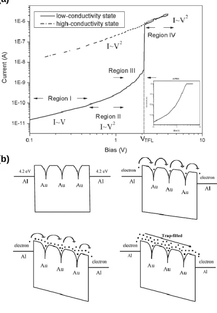
Moreover, the conduction mechanism in polymer-particle nano-trap RRAM has been investigated in details experimentally and theoretically. In the Al/AuNP:PS/Al memory device, AuNP exhibits a work function of around 5.1 eV, which is lower than the LUMO of PS. Therefore, AuNP can be treated as a trap in PS. As a consequence, the current in the memory, as shown in Figure 1.6, can be summarized to regions I (Ohmic conduction with high resistance), II (SCLC model), III (almost fill up traps, and the current is proportional to exponential of voltage), and IV (Ohmic conduction with low resistance) which is indicated the switching mechanism be explained by the
17
Trapping-Detrapping mechanism.48
Figure 1.5. (a) Operational mechanism of the memory. Experimental and fitted J–V curves of the ITO/PFOxPy/Al device (b) OFF state with the Ohmic current (<1.3 V) and SCLC (1.3–2.6 V) models, (c) ON state with the Ohmic current model (>2.8 V).
18
(a)
(b)
Figure 1.6. (a) I–V (in log scale) curves of the Al/Au:NP/Al bistable memory device.
(b) Schematic band diagrams for the transport mechanism of trap-filled SCLC: (i) Region I: thermally generated carrier conduction, (ii) Region II: with traps, (iii) Region III: nearly filled, and (iv) Region IV: traps filled.
1.3.3 Charge Transfer Mechanism
The charge transfer (CT) complex is defined as an electron donor (D)–electron acceptor (A) complex, characterized by electronic transition(s) to an excited state in which there is a partial transfer of electronic charge from the donor to the acceptor moiety.49 The switching and electrical memory phenomena of CT complexes was
19
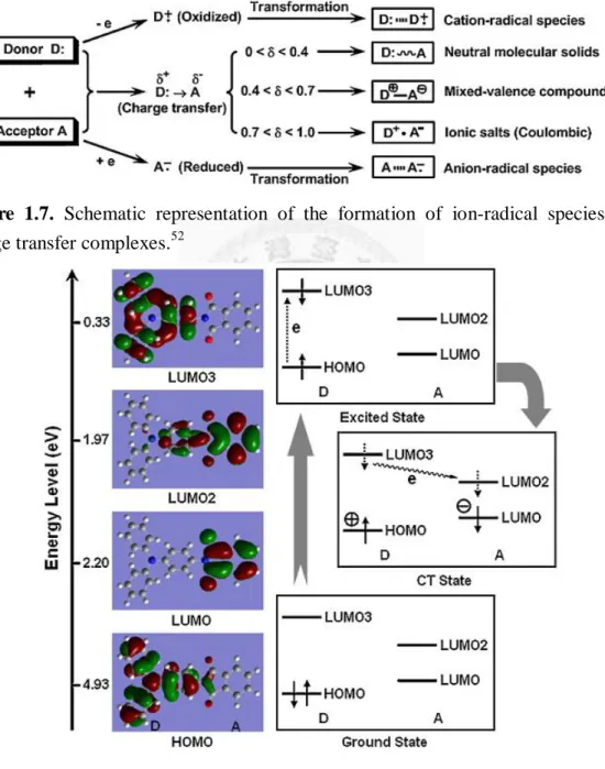
observed in Cu-TCNQ system in the first instance.50 Subsequently, a wide variety of organometallic and all-organic CT complexes have been synthesized for applying in non-volatile organic memories.51 The formation of an organic conductor from a donor, acceptor, and mixed donor–acceptor molecules is depicted schematically in Figure 1.7.52
For a stable CT material, a relationship between ionic binding and conductivity exists. For instance, in the 1:l TCNQ charge transfer salts, donors, which are characterized by small size and low ionization potential, form strongly ionic salts with TCNQ. Under this situation, there is complete charge transfer (or with the CT degree value, δ > 0.7) from the donor to TCNQ and, therefore, these ionic salts are insulators (due to Coulomb interactions). On the opposite, donors which are too large and/or with too high ionization potential will result neutral molecular solids (δ < 0.4). In particular, the situation between above two extreme situations, donors with intermediate size and ionization potential tend to form weakly ionic salts with TCNQ.
These partially ionic, mixed-valence salts tend to have incomplete charge transfer (0.4<δ <0.7) and are likely to exhibit high conductivity.52-54
Functional polyimide containing donor and acceptor moieties has been firstly applied to polymeric memory device by Kang et al. They investigated the charge transfer route induced by the electrical field, which is demonstrated in Figure 1.8, then reported a DRAM fabricated by TP6F-PI.55-56 Triphenylamine (TPA) plays the role of electron donor, and the phthalimide ring acts as electron acceptor. According to the result of molecular simulation performed by Gaussian package program by means of the density functional theory (DFT) method at the B3LYP level of theory (Beckesstyle three-parameter density functional theory using the Lee-Yang-Parr correlation functional) with the 6-31G(d) basic set, the HOMO is located on donor moiety meanwhile the first and second LUMOs are located on acceptor moiety. Charge
20
transfer can occur indirectly, some electrons at the HOMO will transfer to the empty LUMO3 within the donor moiety to form excited state then to LUMO for becoming charge transfer state at the threshold voltage. However, charge transfer can also occur directly from HOMO to LUMO2 and LUMO then become conductive CT complex.
As the result, the device will be switched from OFF state to ON state.
Figure 1.7. Schematic representation of the formation of ion-radical species and charge transfer complexes.52
Figure 1.8. Molecular orbitals (left) of the basic unit of TP6F–PI and the transitions (right) from the ground state to the charge transfer state induced by the electric field.56
21
1.4 Evolution of Polymer Memory
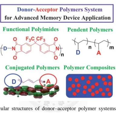
The donor–acceptor containing polymers are widely researched recently for resistive switching memory applications including polymer composites conjugated polymers, non-conjugated pendent polymers, and functional polyimides, as shown in Figure 1.9.57
Figure 1.9. Molecular structures of donor–acceptor polymer systems for advanced memory device applications.57
1.4.1 Polymer Composites
The hybrid composites were extensively prepared for memory device applications.
The supplementary component such as organic molecule or nano materials could be viewed as the data storage media or have the electronic activated domain which is dispersed in the polymer matrix. The operating mechanism of polymer hybrid composite can be attributed to charge transfer or trapping-detrapping for memory application. The domain size of the electronic activated material in the polymer matrix is the key issue for the nano-scale memory device.
22
Yang and co-workers proposed the memory device based on blending well-dispersed capped-gold (Au) nano-particles and aromatic 8-hydroxy quinoline (8-HQ) compound within a polystyrene (PS) matrix.31 Furthermore, small organic molecule can be also regarded as the charge transfer medium, for example, they subsequently reported another organic electrically bistable nonvolatile WORM device based on PCBM:TTF:PS composited film. The operating mechanism is attributed to field induced charge transfer from the donor TTF to acceptor PCBM.58
Afterward, Kang’s group proposed the PVK-CNT composite based memory devices. The devices exhibit insulator, WORM, and conductor controlled by the amount of CNT in the hybrid film. The switching mechanism of the WORM device can be considered as electronic trapping in the carbon nanotubes within the both electronic donating and hole transporting PVK matrix.59 Moreover, functional block copolymers were a candidate for hybrid composite memory devices due to the ability to control the domain size of the fullerene through certain physical interaction.60 1.4.2 Conjugated Polymers
It has long be known, kinds of π-conjugated polymeric materials have been developed for memory devices applications. The sandwich device ITO/PFOxPy/Al, containing electron donor (fluorine moiety) and electron acceptor (oxadiazole and bipyridine moieties), could be switched from the low conductivity state to the high conductivity state. The device exhibit low reading, writing, erasing voltages and a short retention time of the ON state. Therefore, this conjugated copolymer fulfilled the requirement for DRAM. The switching behavior was explained by trapping-detrapping mechanism.61
Moreover, the fluorene and pendent TPA donors and pyridine acceptors containing conjugated polymer F12TPN was applied for WORM memory device. The injected hole could pass through the positive continuous channel along the polymer chain then
23
be trapped by the pyridine acceptors. The detrapping process of the filled traps could not be easily proceed via any process, leading to the WORM property.62
Besides, the device based on conjugated poly[9,9-bis (4-diphenylaminophenyl)-2,7-fluorene] donors covalently bonded with Disperse Red 1 acceptors (DR1-PDPAF-DR1) possessed the fresh type memory characteristic. The electron at HOMO could be excited then transfer to LUMO1 or LUMO2 and raised the conductivity resulted from the charge separation state.63 Furthermore, TPA-based conjugated polyazomethine covalently grafted with graphene oxide (TPAPAM-GO) was designed for non-volatile rewritable memory application. Electrons migrated from the HOMO of the hole transporting polymer TPAPAM into LUMO of graphene layer by intramolecular CT interaction then provided the charge transport pathways and switched the device from the OFF to ON state. The excited electron can be separated and delocalized in graphene nanosheets then stabilize the CT state of TPAPAM-GO, resulting the non-volatile characteristic.64
Meanwhile, a typical WORM memory device could be derived from polyfluorene based copolymers containing the pendent electron-donating TPA and electron-withdrawing cyano groups. The operating mechanism was resulting from the positive charges on the TPA or fluorene moieties were rapidly consumed by the cyano groups then caused the increase in conductivity.65
On the other hand, Ree’s group reported all π-conjugated polymer based on poly(diethyl dipropargylmalonate) (PDEDPM), or polyaniline (PAN) derivatives applying in RRAM devices. These devices include DRAM and WORM type depending on the film thickness.66
In general, the introduction of variety electron acceptors into conjugated polymeric donors significantly influences the memory behaviors, which can either furnish a extra trapping site or provide the CT conducting channel in the electrical switching.
24
The stability of charge trapping or CT complex process governs the volatility of memory device.
1.4.3 Non-conjugated Polymers With Specific Pendent Groups
A wide range of vinyl polymers consisted of side-chain donor–acceptor have been intensively investigated and used for memory applications. As the non-conjugated polymers generally exhibit greater solubility than conjugated polymers, which is facilitating their application to solution-processed memory devices. According to this view point, vinyl polymers containing charge transported pendant groups have been explored for memory application.
The carbazole groups were widely used in the molecular design as the role for electron-donating and hole-transporting and the corresponding memory effect was obtained by incorporating suitable acceptors in the structures. Kang and coworkers designed the non-conjugated copolymers containing pendent carbazole donor and europium complex acceptor (PKEu) that could reach the requirement of non-volatile electrically bistable memory devices.67 Furthermore, the additional incorporation of the pendent 1,3,4-oxdiazole (Ox) group into methacrylate copolymer consisting of a carbazole and Eu complex, named PCzOxEu, exhibited a significant improvement in performance under ambient conditions, leading to a longer retention time and higher ON/OFF current ratio.68 At the threshold voltage, the resultant CT complex create numbers of conducting channels which is mainly caused by holes hopping between the neighboring carbazole units) switched the device to the ON state.34,69 The large dipole moment of the Ox moiety acted as a mediator to decrease the internal energy barrier and facilitate carrier transport, which gave assistance to keep of the separated charges for the longer retention time with improved device stability.68 The same group also incorporated C60 into PVK with covalent bond as the electron acceptor. The
25
device of Al/PVK-C60/ITO performed as nonvolatile flash memory. The CT occurs when then voltage bias is applied then forms the conducting channels by charged HOMO of Cz and charged LUMO of C60.34
Meanwhile, Chen’s group reported the nonconjugated polymers containing pedent electron-donating carbozole units (VPK) and electron-withdrawing oxadiazole derivatives units (OXD or BOXD) with different donor/acceptor ratios for memory device applications.69 The low HOMO energy level of OXD or BOXD units as compared to VPK units created the extra trapping environment. Therefore, distinct electrical characteristics changed between the diode, volatile memory, and insulator tuning by the ratios of donor/acceptor. The unstable ON state of volatile nature SRAM in the P(VPK8OXD2) or P(VPK8BOXD2) device was due to the shallow trapped holes with spontaneous back transferring of charge carriers when removing the electric field.38 Besides, the tunable switching behaviors were explored through the distinct ratio of pendant TPA donors and BOXD acceptors.70 The relative extent of charge trapping/spontaneously back-transferring of trapped carriers controlled the switching behavior. The additional pendent cyano substituted TPA donors groups exhibited NDR behavior probably due to the interaction of the Al atoms with the cyano group.70
Moreover, other pendant group containing nonconjugated polymers such as grafted PVK (PVDR) substituted by CN or NO2 as acceptor,71 pendent azobenzene chromophores for D-A structures,72,73 demonstrated the nonvolatile characteristic, the donor and acceptor moieties played the roles in elucidating the mechanism of charge transfer or space charges and traps effect for the switchable polymers.
26
1.4.4 Functional High Performance Polymers
Functional high performance polymers such as polyimides (PI), polyamide (PA) are favorable materials for microelectronic device applications due to their high performance properties. Therefore, various investigations among the development of all types of PI switching behaviors have been reported widely.
The idea of using functional PI as active layer for memory application was first emerged in 2006 reported by Kang’s group. TP6F-PI with TPA moieties as electron donor and phthalicimide ring as electron acceptor exhibited DRAM behavior.56 Moreover, they found that the conformational change between donor and acceptor moieties induced by charge transfer could provide an energy barrier for back electron transfer from CT state to ground state then extend the retention time of the ON state.74 Both OXTA-PI and AZTA-PI containing pendent TPA donor exhibit WORM memory characteristic in Al/polymer/ITO sandwich devices due to the orthogonal overlap in orbitals between acceptor and pendant donor which could provide a higher energy barrier for back transfer further maintain the device in the ON state after removing the applied electrical field.75.76 Furthermore, Chen and Ueda reported the polymer memory devices based on PI(AAPT-6FDA) derived from
4-amino-4’-(p-aminophenoxy)triphenylamine (AAPT) and
4,4’-(hexafluoroisopropylidene)diphthalic anhydride (6FDA) and PI(APT-6FDA) from 4,4’-bis(p-amino-phenoxy)triphenylamine (APT) and 6FDA. The main difference between two polymer is there are two phenoxyl linkages (L) between TPA (D) and phthalimide (A) moieties in PI(APT-6FDA) but only one in PI(AAPT-6FDA). According to their results, the PI(APT-6FDA) containing (L-D-L-A)n structure showed a SRAM property and PI(AAPT-6FDA) containing (D-L-A)n structure revealed a DRAM property. The dual-mediated phenoxyl linkage of PI(APT-6FDA) led to the more twist conformation compared to the
27
monosubstituted PI(AAPT-6FDA). It thus produced a higher energy barrier then delaying back CT and the elucidated the SRAM behavior.77
Moreover, Ree and our lab fabricated polymer memory device based on TPA containing polyimide system, the results showed that the memory device exhibited nonvolatile write-once-read-many-times (WORM) and volatile DRAM (dynamic random access memory) characteristics depending on the thickness of polymer films.78 Recently, our lab reported that the functional polyimide (OMe)2TPPA-6FPI (6FPI) and the polyamide (OMe)2TPPA-6FPA (6FPA) consisting of electron-donating N,N’-bis(4-aminophenyl)-N,N’-di(4-methoxylphenyl) and 1,4-phenylenediamine [(OMe)2TPPA-diamine] for memory application. 6FPI exhibited dynamic random access memory (DRAM) performance, whereas 6FPA showed static random access memory (SRAM) behavior. The probable reasons are that the 6FPA structure exhibits higher dipole moment and nonplanar linkage resulted in specific SRAM property, which was different from (OMe)2TPPA-6FPI system.79 Moreover, for comparison study in acceptor effect, the corresponding (OMe)2TPPA-ODPI (ODPI), (OMe)2TPPA-DSPI (DSPI), (OMe)2TPPA-PMPI (PMPI), and (OMe)2TPPA-NPPI (NPPI) with different dianhydride moiety were synthesized for memory device application. With the electron-withdrawing moiety intensity of polyimides increasing, the retention time of corresponding memory device increases. ODPI didn’t have memory properties, and PMPI with stronger electron-withdrawing linkage revealed SRAM behavior. NPPI with the strongest electron-withdrawing linkage showed WORM type non-volatile memory behavior. Interestingly, DSPI have the LUMO energy levels between 6FPI and PMPI but revealed non-volatile WORM behavior resulting from the highest dipole moment 5.45D.80
28
1.5 Research Motivations
Donor-acceptor containing polymers have shown great potential for digital memory devices applications. However, the relations between effect of donor-acceptor in the molecular structure and their memory properties have not been fully investigated systematic. Therefore, the primary goal of this thesis is to design and synthesize series of high performance aromatic polymers containing different donor and acceptor moiety or different linkage group between donor and acceptor for discussing the donor-acceptor and linkage group effect to the memory property.
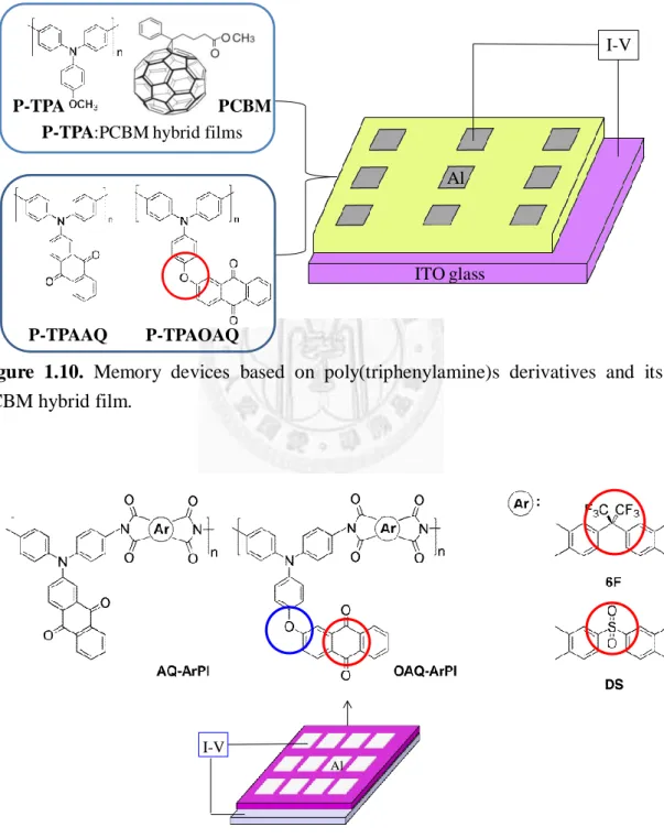
In the first part, we would to explore two distinct approaches, as shown in Figure 1.10, to fabricate the memory devices by blending the PCBM as the acceptor with the donor-containing P-TPA, or incorporating the electron acceptor anthrquinone covalently resulting P-TPAAQ and P-TPAOAQ, respectively. The goal of this part of research is developing the tunable memory characteristics due by the structural design of the electrical functionality and linkage group effect of the TPA-based polymer and morphological control over the embedded PCBM.
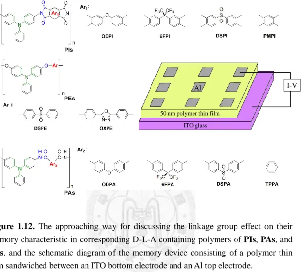
The TPA-containing with dual electron acceptor polyimides AQ-PIs and OAQ-PIs as shown in Figure 1.11, were used to fabricate the memory devices. In addition to the carbonyl or phthalimide acceptor moiety in main chain, the anthraquinone as pendent acceptor group was also introduced to TPA via ether linkage or directly attached into the backbone. The electron charge withdrawing capability of these two acceptors could be studied by molecular simulation, electrochemical, and spectroelectrochemical behaviors. Linkage effect and the electron-withdrawing effect would be investigated in second part of this thesis.
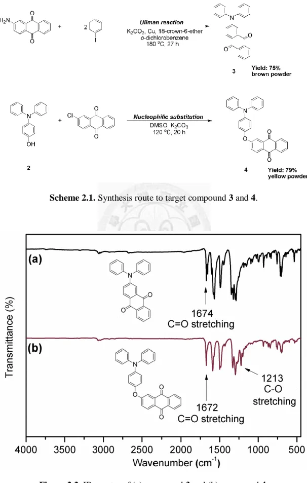
In the final topic of this thesis, three series of polymers with same TPA donor but containing different acceptor or different linkage group between donor and acceptor
29
unit, as shown in Figure 1.12, will be prepared for high-performance polymeric memory devices and the following measurements. Then, the effect of different electro-withdrawing ability or different chain conformation caused distinct linkage group to their memory properties would be investigated systematically.
I-V
Al
ITO glass P-TPA:PCBM hybrid films
P-TPAAQ P-TPAOAQ PCBM P-TPA
Figure 1.10. Memory devices based on poly(triphenylamine)s derivatives and its PCBM hybrid film.
Al
I-V
Figure 1.11. Memory devices fabricated by functional polyimide containing TPA with dual competitive electron acceptors.
30
Al I-V
ITO glass 50 nm polymer thin film PIs
PEs
PAs
High Performance Polymers With Different D-L-AContaining
for Memory Application
Figure 1.12. The approaching way for discussing the linkage group effect on their memory characteristic in corresponding D-L-A containing polymers of PIs, PAs, and PEs, and the schematic diagram of the memory device consisting of a polymer thin film sandwiched between an ITO bottom electrode and an Al top electrode.