國立臺灣大學電機資訊學院電信工程學研究所 碩士論文
Graduate Institute of Communication Engineering College of Electrical Engineering and Computer Science
National Taiwan University Master Thesis
採用主動式電感或平衡非平衡轉換器實現之射頻放大器
RF Amplifiers with Active Inductors or Balun
余超塵 Chau-Chan Yui
指導教授:江簡富 博士
Advisor: Jean-Fu Kiang, Ph.D.
中華民國 101 年 8 月
Aug, 2012
摘要
本論文運用主動式電感、差動主動式電感以及主動式平衡非平衡 轉換器在低雜訊放大器與功率放大器晶片設計上。
其一為運用主動式電感於超寬頻低雜訊放大器上,其中主動式電 感架構包含一組疊接電晶體及一回授電阻來提昇操作頻率,並在回授 路徑上加入共汲極放大器來提高電感 Q 值。實現之晶片面積為 840μm × 610μm,模擬增益在操作頻寬 (3.1-10.3 GHz) 內為 13.68 dB,輸入及輸出反射參數皆小於-10 dB,功耗為 14.02 mW。
其二為運用差動主動式電感之 5 GHz 差動低雜訊放大器,該差 動主動式電感使得晶片面積縮小為 750μm × 600μm,模擬增益在操 作頻率為 12.5 dB,雜訊指數為 2.7 dB,輸入及輸出反射參數皆小於 -10 dB,功耗為 14.2 mW。
其三為運用主動式平衡非平衡轉換器實現之單端輸出功率放大 器。與被動式平衡非平衡轉換器相比,其面積縮小許多。全晶片面積 為 850μm × 650μm,模擬輸出P1dB在操作頻率 5 GHz 為 13.1 dBm,
增益為 26.25 dB,PAE 為 27.9%。
Abstract
An ultra-wideband low-noise amplifier with active inductor is designed and implemented in
a TSMC 0.18µm CMOS technology. This active inductor consists of a cascode FET with a
feedback resistor, and operates at a high self-resonance frequency. The common-drain FET
in the feedback loop enhanced the Q factor of the inductor. The core chip size is only 840
µm × 610 µm. The simulated power gain is 13.68 dB, with the 3-dB bandwidth of 3.1-10.3
GHz. Both the input and ouptut reflection coefficients are less than −10 dB over the entire
band. The power consumption, without an output buffer, at 1.8-V supply is 14.016 mW.
A differential low-noise amplifier at 5 GHz is designed and implemented in a TSMC
0.18µm CMOS technology. The chip size is reduced by using a pair of differential active
inductors with enhanced Q factor and high resonant frequency. The core chip area of this
LNA is 0.45 mm2, the simulated power gain is 12.5 dB, the noise figure is 2.7 dB. Both
the input and ouptut reflection coefficients are below −10 dB over the entire band, and the
power consumption is 14.2 mW.
A CMOS single-ended power amplifier with an active input balun is designed and imple-
mented in a TSMC 0.18µm CMOS technology, which can be implemented in a smaller chip
compared with conventional balanced or differential power amplifiers with a passive output
balun or off-chip transformer. The proposed power amplifier is fabricated using a TSMC
0.18 µm CMOS process. Its chip size is 0.85 µm × 0.65 µm, the output P1dB is 13.1 dBm,
its gain is 26.25 dB, and its PAE of 27.9 %.
Contents
Abstract i
Table of Contents iv
List of Figures vi
List of Tables vii
Acknowledgment viii
1 Introduction 1
2 Ultrawideband Low-Noise Amplifiers with Active Inductors 5
2.1 Circuit Design . . . 5
2.2 Results and Discussions . . . 9
3 Differential Low-Noise Amplifier at 5 GHz with a Differential Active In-
ductor 12
3.1 Circuit Design . . . 12
3.2 Results and Discussions . . . 16
4 5 GHz CMOS Single-ended Power Amplifier with an Active Balun 20
4.1 Circuit Design . . . 20
4.2 Results and Discussions . . . 24
5 Conclusion 26
Bibliography 28
List of Figures
2.1 Proposed schematic of the LNA incorporating an active inductor. . . 6
2.2 Active inductor with a gyrator-C topology [12]. . . 6
2.3 Schematic of an active inductor: (a) plain version in [1], (b) enhanced-Q version proposed in this work, (c) equivalent circuit of either (a) or (b). . . . 7
2.4 Layout of the proposed LNA. . . 9
2.5 Simulated S21 (——) and S11 (− − −) of the proposed UWB LNA. . . 9
2.6 Simulated noise figure of the proposed UWB LNA. . . 10
3.1 Differential LNA with a differential active inductor. . . 13
3.2 A pair of differential active inductors consisting of two half-circuits. . . 13
3.3 Active inductor in a gyrator-C topology [12]. . . 13
3.4 Schematic of a half-circuit in Fig. 3.2, without the negative resistance −1/(2gm10): (a) plain version in [1], (b) enhanced-Q version proposed in this work, (c) equivalent circuit of either (a) or (b). . . 14
3.5 Chip layout. . . 17
3.6 Simulated S11 ( —— ) and S21 (− − −) of the LNA. . . 17
3.7 Simulated noise figure of LNA. . . 18
4.1 Schematic of single-ended power amplifier with an input balun. . . 20
4.2 Simulated power gain and output power of the active balun. . . 21
4.3 Simulated PAE and power gain of the one-stage single-ended cascode power amplifier, ——: power gain, − − −: PAE. . . 21
4.4 Simulated output power versus input power of the one-stage single-ended cas- code power amplifier. . . 22
4.5 Chip layout. . . 22
4.6 Simulated PAE and power gain of the proposed power amplifier, ——: power gain, − − −: PAE. . . 23
4.7 Simulated output power versus input power of the proposed power amplifier. 23
List of Tables
2.1 Performance comparison of UWB LNA. . . 11
3.1 Performance comparison with literatures. . . 18
4.1 Performance comparison with single-ended Power Amplifier. . . 24
Acknowledgment
First of all, I would like to express my sincerest thanks to my thesis advisor, Professor Jean-
Fu Kiang, for his advices and supports throughout the past two years to pursue my master
degree. His exciting lectures, enthusiastic attitude, and research experiences motivate me
to enhance my understanding on electromagnetic theories and their applications. I am also
grateful to my thesis readers, Professor A and Professor B for their valuable comments to
improve the quality of this thesis. I would like to thank the faculty in the Department of
Electrical Engineering and the Graduate Institute of Communication Engineering, Nation
Taiwan University for many useful courses they offered. My classmates and friends in the
graduate school are also appreciated for their friendship in these two years. The deepest
appreciations are owed to my parents for their considerations and encouragement. They
always support me to pursue this master degree, and I am pleased to share this honor with
them.
Chapter 1 Introduction
In typical chips of RF/microwave circuits, spiral inductors usually take most of the chip
area. An active inductor made of transistors can significantly reduce the chip area. In [1],
two cascode FET’s and a feedback resistor make up an effective broadband active inductor.
Compared with passive inductors, active inductors usually have a wider range of tunability.
In [2], a bias current is used to adjust the gain and bandwidth of the active inductors to
tune in different bands of an ultra-wideband (UWB) MB-OFDM system.
In an UWB system, the low-noise amplifier (LNA) is required to have low noise, wide
bandwidth, high and flat gain, and low power consumption. Many reported full-band LNAs
for UWB are implemented in a common-source or cascode topology to achieve broadband
impedance matching. However, such an architecture bears high noise figure (NF) at high
frequencies due to their dependence on the cutoff frequency [3].
A two-stage LNA, made of a common-gate (CG) stage in cascade with a cascode (CG on
top of CS) stage, is reported to have constant NF over the full band [4]. The common-gate
stage has a constant wideband input impedance of 1/gm, with gmthe transconductance of the
transistor. In general, the inter-stage matching network between the common-gate stage and
the cascode stage takes two inductors to implement. The active inductor is non-reciprocal,
hence is not suitable for this configuration.
In [5], an UWB LNA is achieved by combining a narrowband LNA with a resistive
shunt-feedback. Passive components are required for input matching, and the non-reciprocal
active inductors are not applicable. However, it needs only one shunt peaking inductor at
the output of the first stage, which can be implemented using an active inductor.
A wideband LNA with current-reuse cascade configuration is proposed in [6]. The wide-
band input impedance matching is achieved by using a resistive shuntVshunt feedback path
in conjunction with a parallel LC load, making the input network equivalent to two parallel
RLC tanks. If the three passive inductors in the first stage are to be replaced, a cascode of
8 transistors are required, which demands a very high dc voltage.
A low-noise amplifier (LNA) usually serves as the first functional module of a wireless
receiver. It is required to amplify the received signal while contributing as little noise as
possible. Common-source (CS) LNA’s [7], [8] have been widely used due to its good noise
performance. A common-gate (CG) LNA can achieve the input impedance matching more
easily, but its noise performance is relatively poorer [9]. Applying a cross-coupling technique
on a CG-LNA [10] helps improve its noise performance by partially canceling the noise
contribution of the common-gate transistor. On the other hand, the existence of parasitic
capacitance at the source of the cascode transistor degrades the noise performance of a
CS-LNA [11].
In the implementation of typical RF/microwave chips, spiral inductors usually take most
of the chip area. Active inductors made of transistors are smaller than their passive coun-
terparts, especially at low frequencies. In [1], two cascode FET’s and a feedback resistor
are used to make up a broadband active inductor. Compared with passive inductors, active
inductors also have a wider range of tunability. Active inductors have also been realized
using a gyrator-C topology, where the gyrator consists of two transconductors connected in
a feedback configuration [12].
Highly integrated and low-cost transmitters based on CMOS process have been exten-
sively developed [13], [14]. Both on-chip and off-chip passive transformers have been used
to build a balun to convert between differential signals and single-ended signal flowing in a
transmitter. A passive balun implemented with on-chip inductors has a significant loss and
takes a considerable chip area. Off-chip transformers incur considerable cost and is much
larger in size.
In [15], a fully differential cascode topology, composed of a driver and a differential power
amplifier (PA), is proposed to achieve high efficiency and reliable operation. An external low-
loss commercial balun made of lumped elements is adopted to convert the differential output
to a single-ended signal. In [16], a double cascode PA with switched programmable feedback
biasing is integrated with a balun for embedded WLAN applications. In [17], a differential
auto-transformer is used as an output balun to build an integrated power amplifier. The
auto-transformer balun incurs low power loss, hence increasing the saturated output power
and reducing the gain compression. In [18], an on-chip active balun is used to replace
the quadrature coupler which is needed in a conventional Doherty power amplifier, and
substantially increase the power gain of the latter. In [19]- [21], the differential output from
the up-conversion mixer is converted to a single-ended signal, using a balun of transformer
structure, before being sent to a power amplifier.
Chapter 2
Ultrawideband Low-Noise Amplifiers with Active Inductors
2.1 Circuit Design
In this work, an UWB LNA in 3-10 GHz is designed, which contains two active inductors and
two passive inductors. Fig. 2.1 depicts the schematic of the proposed LNA which consists of
a common-gate stage, a cascode stage with an active inductor load, and a buffer. In order not
to increase the noise figure, the inter-stage matching inductors L2 and L3 are implemented
with conventional coils.
Fig.2.2 depicts an active inductor with a gyrator-C topology, in which the gyrator is
consisted of two transconductors connected in a feedback configuration [12], where Gm1 and
Gm2 are transconductance, Go1 and Go2 are output conductance, C1 and C2 are output ca-
pacitance of these two amplifiers. It is called an active inductor because the input impedance
Zin of the gyrator loaded with a capacitor is inductive. The input impedance Zin can be
derived from a small-signal model which is equivalent to a parallel RLC circuit of resonant
Figure 2.1: Proposed schematic of the LNA incorporating an active inductor.
Figure 2.2: Active inductor with a gyrator-C topology [12].
(a) (b)
(c)
Figure 2.3: Schematic of an active inductor: (a) plain version in [1], (b) enhanced-Q version proposed in this work, (c) equivalent circuit of either (a) or (b).
frequency ω0 = 1/
√
LC and quality factor Q = ω0L/R = ω0RC [12].
Fig.2.3(a) shows an active inductor proposed in [1], Fig.2.3(b) shows an enhanced-Q
version proposed in this work, to improve the gain of the designed LNA. Fig.2.3(c) depicts
an equivalent circuit of either Figs.2.2, 2.3(a) or 2.3(b). The equivalent-circuit parameters
related to Fig.2.2 are
Rs' Go1
Gm1Gm2
, Lp ' C1
Gm1Gm2
Cp ' C2, Rp ' 1 Go2
(2.1)
Since Zind is inductive below ω0 and is capacitive above ω0, a high ω0 is preferred to achieve
an equivalent inductor over a wide frequency range.
Compare Fig.2.3(a) with Fig. 2.2, we have Gm1= gm1, Gm2 = gm2, C1 = Cgs1, C2 = Cgs2,
Go1= go1, Go2' 0. Thus, (3.1) can be reduced to
Rs ' go1
gm1gm2
, Lp ' Cgs1
gm1gm2
Cp ' Cgs2, Rp ' ∞ (2.2)
If an FET is characterized by its transconductance gm and gate-source capacitance Cgs
only, the input impedance Zin1 of the active inductor shown in Fig.2.3(a) can be represented
as
Zin1 = 1 gm1
1 + jωCgs1Rf
1 + jω Cgs1
gm1
− Cgs2
gm1
+ ω2Cgs1Cgs22 g2m1gm2
! (2.3)
where the subscripts 1 and 2 referred to M1 and M2, respectively. If ω2Cgs1Cgs22 g2m1gm2
1, Zin1
reduces to Zind of Fig.2.3(c), with component values listed in (3.2).
Similarly, the input impedance of the active inductor shown in Fig.2.3(b) can be expressed
as
Zin2 = Cgs1Cgs2
gm1gm2gm3
go3go1
Cgs1Cgs2
+ jω go1
Cgs2
+ gm1
Cgs1
!
− ω2gm3Rf
1 + jω Cgs1go1
gm1gm2
+ Cgs2
gm2
− ω2Cgs1Cgs2
gm1gm2
! (2.4)
which is the same as Zind of Fig.2.3(c) with
Rs ' go2go3
gm1gm2gm3
, Lp ' Cgs2
gm2gm3
g
Figure 2.4: Layout of the proposed LNA.
Figure 2.5: Simulated S21 (——) and S11 (− − −) of the proposed UWB LNA.
Noe that Rs in (3.5) is smaller than that in (3.2) by a factor of go2go3/(go1gm3), which is on
the order of 100, due to the feedback tansistor M3. Hence, a much higher Q-factor can be
achieved.
2.2 Results and Discussions
Fig.2.4 shows the layout of the proposed LNA. Its area, including all bonding pads, is 840
µm × 610 µm. The amplifier will be measured via on-wafer probes. Fig.2.5 shows that the
simulated gain S21 is 9.3-13.6 dB with the 3 dB bandwidth of 3-10.3 GHz. Fig.2.6 shows the
Figure 2.6: Simulated noise figure of the proposed UWB LNA.
simulated noise figure, which is 3.77-4.79 dB over 3.0-10.3 GHz. Table 4.1 summarizes the
performance of this LNA, compared with other works in the literatures. Note that the dc
voltage level at the second-stage output is restricted to a lower level to coordinate with the
bias of the active inductor. Hence, the linearity becomes poorer when the output ac signal
becomes strong. Compare with the LNA using passive inductors in 4.1, LNA’s incorporating
active inductors take more power and present higher noise. The proposed LNA has a smaller
chip size, slightly lower noise figure and higher gain than those in [5] and [24]. The design
in [22] consumes almost three times of power as in our chip. Although its gain is at least 3
db higher, its bandwidth is narrower than ours, and its noise figure is higher than ours. The
chip area in [23] does not include the bonding pads. Its power consumption is higher than
our design, but its gain and noise figure are poorer than our design.
Table 2.1: Performance comparison of UWB LNA.
Parameter This work
This work with AI re-
placed by passive one
JSSC04 [5]
JSSC05 [22]
MTT08 [23]
JSSC09 [24]
Technology 0.18µm 0.18µmCMOS0.18µm CMOS
0.13µm CMOS
0.09µm CMOS
0.13µm CMOS bandwidth
(GHz)
3.1-10.3 3.1-10.3 2.3-9.2 2.0-5.2 0.2-9.0 1.5-8.1
Gain (dB) 9.3-13.6 9.7-14.6 9.3 16 10.0 11.7
Noise figure (dB)
3.77-4.79 2.5-3.3 4.0-9.2 4.7-5.7 5.0-8.0 3.6-6.0
IIP3 (dBm) −9 −4 −5 N/A +1 +8
Power cons.
(mW)
14.02 11.2 9 38 20 2.62
Chip size (mm2)
0.512 (die)
N/A 0.66 (die) 0.24 (die) 0.066 (core)
0.58 (die)
Chapter 3
Differential Low-Noise Amplifier at 5 GHz with a Differential Active
Inductor
3.1 Circuit Design
In this work, a 5 GH differential LNA in a cascode configuration is proposed, and differential
active inductors are used to reduce its chip size. Fig.3.1 depicts the schematic of the proposed
LNA in a cascode configuration, with each cascode consisting of a common-source stage and
a common-gate stage. The LNA is loaded with a pair of differential active inductors. In
order not to incur much noise, passive inductors at the input matching network are not
replaced by their active counterparts.
Fig. 3.2 shows the schematic of the differential active inductors proposed in this work,
which is consisted of two identical half-circuits.
Fig.3.3 depicts an active inductor in a gyrator-C topology. The gyrator is consisted of
two transconductors G and G , connected in a feedback configuration [12], where G
Figure 3.1: Differential LNA with a differential active inductor.
Figure 3.2: A pair of differential active inductors consisting of two half-circuits.
Figure 3.3: Active inductor in a gyrator-C topology [12].
(a) (b)
(c)
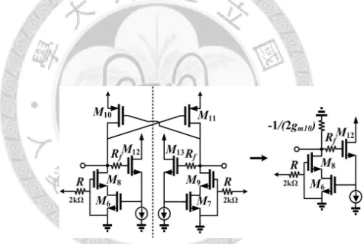
Figure 3.4: Schematic of a half-circuit in Fig. 3.2, without the negative resistance
−1/(2gm10): (a) plain version in [1], (b) enhanced-Q version proposed in this work, (c) equivalent circuit of either (a) or (b).
and Go2 represent output conductances, C1 and C2 represent output capacitances.
Figs.3.4(a) and 3.4(b) show two versions of half-circuit of the differential active inductors
in Fig. 3.2, without the negative resistance −/(2gm10). Fig.3.4(c) depicts the equivalent
circuit of either Figs.3.3, 3.4(a) or 3.4(b). The input impedance Zind emulates that of a
parallel RLC tank with resonant frequency ω0 = 1/
√
LC and quality factor Q = ω0L/R =
ω0RC. The parameters referred to in Fig.3.3 are
Rs ' Go1
Gm1Gm2
, Lp = C1
Gm1Gm2
Cp ' C2, Rp ' 1 Go2
(3.1)
Since Z is inductive below ω and is capacitive above ω , a higher ω is preferred to
implement an inductor over a wider frequency range.
To make Fig.3.4(a) equivalent to Fig. 3.3 implies Gm1 = gm1, Gm2 = gm2, C1 = Cgs1,
C2= Cgs2, Go1= go1, Go2' 0. As a consequence, (3.1) is reduced to
Rs' go1
gm1gm2
, Lp = Cgs1
gm1gm2
Cp ' C2, Rp ' 1 go2
(3.2)
If an FET is modeled by its transconductance gm and gate-source capacitance Cgs only,
the input impedance Zin1 shown in Fig.3.4(a) can be represented as
Zin1 = 1 gm1
1 + jωCgs1Rf
1 + jω Cgs1
gm1
− Cgs2
gm1
+ ω2Cgs1Cgs22 g2m1gm2
! (3.3)
where the subscripts 1 and 2 refer to N1 and N2, respectively, as shown in Fig.3.4(a). If
ω2Cgs1Cgs22 gm12 gm2
1, Zin1will reduce to Zindof Fig.3.4(c), with the component expressions listed
in (3.2).
Similarly, the input impedance of the half-circuit shown in Fig.3.4(b) can be expressed
as
Zin2 = Cgs1Cgs2
gm1gm2gm3
gds3gds1
Cgs1Cgs2
+ jω gds1
Cgs2
+ gm1
Cgs1
!
− ω2gm3Rf
1 + jω Cgs1gds1
gm1gm2
+Cgs2
gm2
− ω2Cgs1Cgs2
gm1gm2
! (3.4)
By setting Zin2 = Zind as in Fig.3.4(c), the component expressions will become
Rs ' go2go3
gm1gm2gm3
, Lp ' Cgs2
gm2gm3
Cp ' go3
gm1
Cgs1, Rp ' gm1
go1go2
(3.5)
Note that Rs in (3.5) is smaller than that in (3.2) by a factor of go2go3/(gm2gm3), which is
on the order of 100, due to the feedback tansistor N3. The reduction of Rs will increase the
Q factor of the active inductor.
Next, consider the effect of the negative resistance −1/(2gm10), as shown in Fig.3.2.
Since this negative resistance is connected to the input port, Zin2, as shown in Fig.3.4(b), it
is also connected to the input port, Zind, as shown in Fig.3.4(c) and shunt to Rp. Thus, the
expressions in Rp of (3.5) are modified as
R0p = Rp
1 1 − 2gm10Rp
(3.6)
To avoid self oscillation due to positive feedback, the condition 2gm10Rp < 1 must be satisfied.
Hence R0p is larger than Rp by a factor of 1/(1 − 2gm10Rp), which further increases the Q
factor of the active inductor.
3.2 Results and Discussions
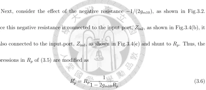
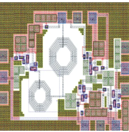
Fig. 3.5 shows the layout of the proposed LNA, which is fabricated in a TSMC 0.18µm
Figure 3.5: Chip layout.
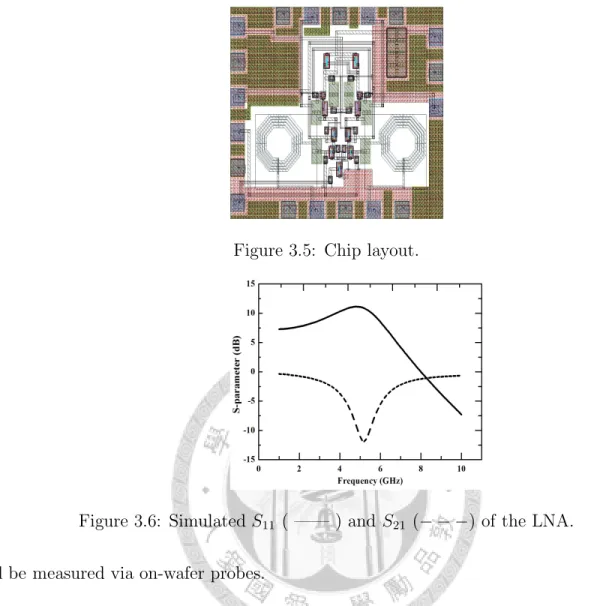
Figure 3.6: Simulated S11 ( —— ) and S21 (− − −) of the LNA.
will be measured via on-wafer probes.
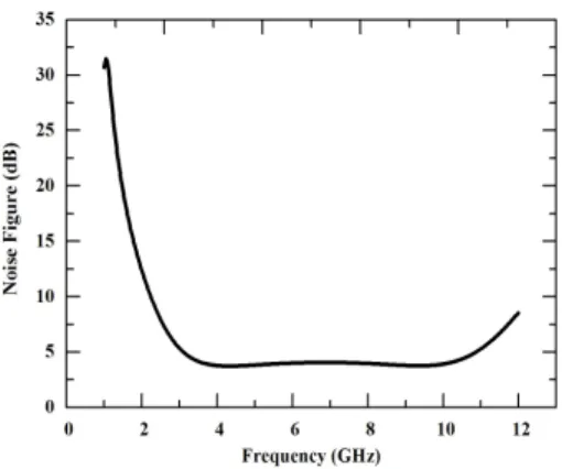
Fig.3.6 shows the gain and the input reflection coefficient of the LNA. Fig.3.7 shows the
simulated noise figure. Within the operation band of 5.2-5.4 GHz, the simulated gain is 12.5
dB, the input reflection coefficient is −15 dB, the simulated noise figure is 2.7 dB, and the
power consumption is 14.2 mW.
Table 4.1 summarizes the performance of this LNA, compared with other works in the
literatures. Note that the dc voltage level of the cascode output is restricted to a lower
level to coordinate with the the dc bias of the active inductor. Hence, the linearity of signal
Figure 3.7: Simulated noise figure of LNA.
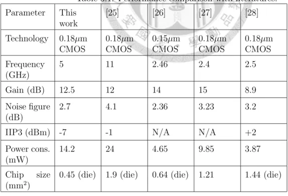
Table 3.1: Performance comparison with literatures.
Parameter This work
[25] [26] [27] [28]
Technology 0.18µm CMOS
0.18µm CMOS
0.15µm CMOS
0.18µm CMOS
0.18µm CMOS Frequency
(GHz)
5 11 2.46 2.4 2.5
Gain (dB) 12.5 12 14 15 8.9
Noise figure (dB)
2.7 4.1 2.36 3.23 3.2
IIP3 (dBm) -7 -1 N/A N/A +2
Power cons.
(mW)
14.2 24 4.65 9.85 3.87
Chip size (mm2)
0.45 (die) 1.9 (die) 0.64 (die) 1.21 1.44 (die)
becomes poorer when the output ac level becomes too high. The proposed LNA has about
one-quarter of chip size, slightly lower noise figure, and lower power consumption than [25].
The proposed LNA has similar performance to that in [26], while the latter is implemented
in 0.15µm CMOS process. Compared with our design, the gain in [27] is 3 dB higher, its
power consumption is 4.5 mW higher, its chip size is about 1.21mm2, and its noise figure is
0.5 dB higher. The design in [28] is a one-stage single-ended cascode LNA. Its chip size is
about three times of our design, it consumes only one-quarter of power as in our design, its
gain and noise figure are worse than our design.
Chapter 4
5 GHz CMOS Single-ended Power Amplifier with an Active Balun
4.1 Circuit Design
In this work, we present a single-ended power amplifier integrated with an active balun, op-
erating at 5 GHz. The active balun is inserted in front of the single-ended power amplifier to
convert the differential input signals to a single-ended signal. Fig.4.1 shows the architecture
of the proposed single-ended power amplifier with an input balun. The active balun used is
this design has the topology of a PMOS current mirror. The transistor N3 is biased to Vg2 to
function as a constant current sink. The differential input signals are amplified via N1 and
Figure 4.1: Schematic of single-ended power amplifier with an input balun.
Figure 4.2: Simulated power gain and output power of the active balun.
Figure 4.3: Simulated PAE and power gain of the one-stage single-ended cascode power amplifier, ——: power gain, − − −: PAE.
N2 which are biased in the saturation region to achieve high linearity. The amplified signals
are combined to a single-ended signal at the output by the PMOS current mirror consisted
of P1 and P2. The linearity of the active balun is traded off with the dc power consumption
by adjusting Vg2.
Fig.4.2 shows the simulated power gain and output power of the active balun. The power
gain is −0.03 dB, its output P1dB is −5.03 dBm.
The power amplifier alone is designed to operate in class-A. The bias circuit of the power
amplifier is used to generate a reference current, which is composed of resistors R1, R2, and
Figure 4.4: Simulated output power versus input power of the one-stage single-ended cascode power amplifier.
Figure 4.5: Chip layout.
transistors N4, N5. The series capacitor C2 and shunt inductor L1 make up an interstage
matching network. Fig.4.3 shows the simulated power gain and power-added efficiency (PAE)
of the power amplifier alone.
Fig.4.4 shows the the simulated output power versus input power. The simulated power
gain is 17 dB, the output P1dB is 15.9 dBm, and the maximum PAE is 41.47 %.
Figure 4.6: Simulated PAE and power gain of the proposed power amplifier, ——: power gain, − − −: PAE.
Figure 4.7: Simulated output power versus input power of the proposed power amplifier.
Table 4.1: Performance comparison with single-ended Power Amplifier.
Parameter This work JSSC08 [15]
RFIC10 [16]
MTT09 [17]
MTT10 [29]
Technology 0.18µm CMOS
0.13µm CMOS
65 nm
CMOS
SiGe:C bipolar
90 nm
CMOS OP1dB
(dBm)
13.1 27.5 18.2-23.2 24.6 N/A
Power gain (dB)
26.25 24 25.3-26.7 13 18
PAE (%) 27.9 48 19-21.1 40 48
Psat (dBm) 16.8 30.5 23.5-28.4 29 32
Chip size (mm2)
0.55 (die) 2.7 (die) 1.2 (die) 1.65 (die) 1.25 (die)
4.2 Results and Discussions
Fig.2.4 shows the chip layout in a TSMC 0.18µm CMOS technology, and the chip size is
0.85 × 0.65 mm2. Fig.4.6 shows that the simulated power gain is 26.25 dB, and the maximum
PAE is 27.9 %. Because the active balun consumes some power and incurs some loss, the
maximum PAE and P1dB are reduced. Fig.4.7 shows the simulated output power versus
input power, and its output P1dB is 13.1 dBm.
This design is compatible with the requirements on band group number 4 (5.016 GHz) of
the 802.15.4a WLAN systems by the FCC, USA [?]: The output spectrum must be less than
−45.3 dBm/MHz. The power amplifier in this design has sufficient output power, linearity
and PAE for this application.
in the literatures. In [15], the die area includes the lumped-element balun which takes about
2 mm2. It is quite obvious that the active balun adopted in our work is much smaller than
this lumped-element version. However, the active balun consumes some power and hence
reduce the PAE.
The chip in [16] does not include the output balun, but its size is still more than twice
of our design. Its Psat and OP1dB are better than our design, but its PAE is poorer. The
differential auto-transformer in [17] increases the saturated output power significantly, but
it takes too much area. In [29], a transformer balun is used for output matching, its PAE
and Psat are bettwer than our design. It uses a more advanced process, but still takes more
than twice of chip area than our design.
Chapter 5 Conclusion
An UWB LAN has been designed with a common-gate stage and a cascode stage. An active
inductor with enhanced Q factor is implemented as the load inductor of the cascode stage.
It helps reduce the chip size while keeping low noise figure and power consumption. The
proposed design is implemented in a TSMC 0.18 µm CMOS technology. Over the 3.1-10.6
GHz band, its maximum gain is 13.6 dB, noise figure is 3.77-4.79 dB, and consumes 7.9 mA
from a 1.8 V supply.
A 5 GHz differential LNA loaded with a pair of differential active indcutors has been
designed and implemented in a TSMC 0.18µm CMOS process. An equivalent-circuit model
is presented to explain the enhancement of Q factor in the design of the active inductors.
The proposed design achieves 12.5 dB gain, 2.7 dB noise fgure at 5 GHz, and dissipates 7.9
mA dc current from a 1.8 V supply. The chip size is reduced by using the differential active
indcutors, and its performance is comparable to those designs using passive inductors.
A compact power amplifier at 5 GHz is designed, in which an active balun is used to
convert the differential input signals to a single-ended signal. This integrated design is
fabricated using a TSMC 0.18µm CMOS process, and its size is 0.85 µm × 0.65 µm. The
output P1dB is 13.1 dBm, its peak gain is 26.25 dB, and its PAE is 27.9 %.
Bibliography
[1] S. Hara, T. Tokumitsu, T. Tanaka, and M. Aikawa, ”Broad-band monolithic microwave
active inductor and its application to miniaturized wide-band amplifiers,” IEEE Trans.
Microwave Theory Tech., vol.36, no.12, pp.1920-1924, Dec. 1988.
[2] M. M. Reja and K. Moez, ”An area-efficient multistage 3.0-to 8.5-GHz CMOS UWB
LNA using tunable active inductors,” IEEE Trans. Circuits Syst. II, vol.57, no.8, pp.587-
591, Aug. 2010.
[3] A. Bevilacqua and A. Niknejad, ”An ultra-wideband CMOS LNA for 3.1 to 10.6 GHz
wireless receivers,” IEEE Int. Solid-State Circuits Conf., pp. 139V140, Feb. 2004.
[4] Y. Shim, C. W. Kim, J. Lee, and S. G. Lee, ”Design of full band UWB common-gate
LNA,” IEEE Microwave Wireless Comp. Lett., vol. 17, no. 10, pp. 721-723, Oct. 2007.
[5] A. Bevilacqua and A. M. Niknejad, ”An ultrawideband CMOS lownoise amplifier for
3.1-10.6-GHz wireless receivers,” IEEE J. Solid-State Circuits, vol.39, no.12, pp.2259-
[6] Y. S. Lin, C. Z. Chen, H. Y. Yang, C. C. Chen, J. H. Lee, G. W. Huang, and S. S. Lu,
”Analysis and design of a CMOS UWB LNA with dual-RLC-branch wideband input
matching network,” IEEE Trans. Microwave Theory Tech., vol.58, no.2, pp.287-296,
Feb. 2010.
[7] D. K. Sheffer and T. H. Lee, ”A 1.5 V, 1.5 GHz CMOS low-noise amplifier,” IEEE J.
Solid-State Circuits, vol. 32, no. 5, pp. 745-759, Oct. 1997.
[8] T. K. Nguyen, C. H. Kim, G. J. Ihm, M. S. Yang, and S. G. Lee, ”CMOS low-noise
amplifier design optimization tehcniques,” IEEE Trans. Microwave Theory Tech., vol.
52, no. 5, pp. 1433-1442, May 2004.
[9] H. Darabi and A. A. Abidi, ”A 4.5 mW 900-MHz CMOS receiver for wireless paging,”
IEEE J. Solid-State Circuits, vol. 35, no. 8, pp. 1085-1096, Aug. 2000.
[10] X. Li, S. Shekhar, and D. J. Allstot, ”Gm-boosted common-gate LNA and differential
Colpitts VCO/QVCO in 0.18µm CMOS,” IEEE J. Solid-State Circuits, vol.40, no.12,
pp. 2609- 2619, Dec. 2005.
[11] T. H. Lee, H. Samavati, and H. R. Rategh, ”5-GHz CMOS wireless LANs,” IEEE Trans.
Microwave Theory Tech., vol. 50, no. 1, pp. 268V280, Jan. 2002.
[12] A. Thanachanont, ”CMOS transistor-only active inductor for IF/RF applications,”
Proc. IEEE ICIT, vol.2, pp. 1209- 1212, Dec. 11-14, 2002.
[13] J. A. Weldon, “A 1.75-GHz highly integrated narrowband CMOS transmitter with
harmonic-rejection mixers,” IEEE J. Solid-State Circuits, vol. 36, no. 12, pp. 2003-2015,
Dec. 2001.
[14] K. Lee, S. Lee, Y. Koo, H. Huh, H. Nam, J. Lee, J. Park, K. Lee, D. Jeong, and W.
Kim, “Full-CMOS 2-GHz WCDMA direct conversion transmitter and receiver,” IEEE
J. Solid-State Circuits, vol. 38, no. 1, pp.43-53, Jan. 2003.
[15] R. Brama, L. Larcher, A. Mazzanti, and F. Svelto, ”A 30.5 dBm 48% PAE CMOS
class-E PA with integrated balun for RF applications,” IEEE J. Solid-State Circuits,
vol. 43, no. 8, pp.1755-1762, Aug. 2008.
[16] M. Y. Li, A. Afsahi, and A. Behzad, ”A single-chip 2.4GHz double cascode power
amplifier with switched programmable feedback biasing under multiple supply voltages
in 65nm CMOS for WLAN application,” IEEE Radio Freq. Integ. Circuits Symp., pp.
391-394, May. 2010.
[17] V. A. Solomko and P. Weger, ”A fully integrated 3.3-3.8-GHz power amplifier with
2172, Sep. 2009.
[18] M. G. Li, Q. R. Wu, and R. Y. Shi, ”2.4 GHz Doherty power amplifier with on-chip
active balun design,” IEEE ASIC Conf., pp.1078-1080, Oct. 2009.
[19] S. Chiu, I. Kipnis, M. Loyer, J. Rapp, D. Westberg, J. Johansson, and P. Johansson,
”A 900 MHz UHF RFID reader transceiver IC,” IEEE Int. Solid-State Circuits Conf.,
pp.214-598, Feb. 2007.
[20] I. Kwon, H. Bang, K. Choi, S. Jeon, S. Jung, D. Lee, Y. Eo, H. Lee, and B. Y. Chung,
”A single-chip CMOS transceiver for UHF mobile RFID reader,” IEEE J. Solid-State
Circuits, vol.43, no.3, pp.729-738, Mar. 2008
[21] K. Choi, S. Yoo, M. Kim, H. Kim, S. Ryu, S. Kang, S. Jung, and Y. Yang, ”CMOS
DSB transmitter with low Tx noise for UHF RFID reader system-on-chip,” IEEE Trans.
Microwave Theory Tech., vol 58, no. 12, pp. 3467-3474, Dec. 2010.
[22] R. Gharpurey, ”A broadband low-noise front-end amplifier for ultra wideband in 0.13-
gm CMOS,” IEEE J. Solid-State Circuits, vol.40, no.9, pp.1983-1986, Sep. 2005.
[23] T. Chang, J. Chen, L. A. Rigge, and J. Lin, ”ESD-protected wideband CMOS LNAs
using modified resistive feedback techniques with chipon-board packaging,” IEEE Trans.
Microwave Theory Tech., vol.56, no.8, pp.1817-1826, Aug. 2008.
[24] H. Zhang, X. Fan, and E. Sanchez-Sinencio, ”A low-power, linearized, ultra-wideband
LNA design techniques,” IEEE J. Solid-State Circuits, vol.44, no.2, pp.320-330, Feb.
2009.
[25] X. W. He, M. X. Zhang, J. W. Li, and S. Q. Li, ”A 11 GHz differential LNA integrated
with on-chip antenna for wireless receivers,” IEEE Custom. Solid-State Integ. Circuit
Technol. Conf., pp.761-763, 2010.
[26] V. Chandrasekhar, ”A packaged 2.4 GHz LNA in a 0.15 µm CMOS process with 2kV
HBM ESD protection,” IEEE Eur. Solid-State Circuits Conf., pp.347-350, Sep. 2002.
[27] C. L. Hsiao, R. M. Weng, and K. Y. Lin, ”A 1 V fully differential CMOS LNA for 2.4
GHz application,” IEEE Circuits Syst. Conf., pp.245-248, Sep. 2003.
[28] B. Toole and C. Plett, ”A low voltage, low power RF CMOS LNA for bluetooth ap-
plications using transmission line transformers,” IEEE Eur. Solid-State Circuits Conf.,
pp.433-436, Sep. 2001.
[29] O. Degani, F. Cossoy, S. Shahaf, E. Cohen, V. Kravtsov, O. Sendik, D. Chowdhury,
C. D. Hull, and S. Ravid, ”A 90-nm CMOS power amplifier for 802.16e (WiMAX)
applications,” IEEE Trans. Microwave Theory Tech., vol.58, no.5, pp.1431-1437, May.
![Figure 2.3: Schematic of an active inductor: (a) plain version in [1], (b) enhanced-Q version proposed in this work, (c) equivalent circuit of either (a) or (b).](https://thumb-ap.123doks.com/thumbv2/9libinfo/9600486.628842/17.918.321.577.130.463/figure-schematic-inductor-version-enhanced-version-proposed-equivalent.webp)
![Table 2.1: Performance comparison of UWB LNA. Parameter This work This work with AI re-placed by passive one JSSC04[5] JSSC05[22] MTT08[23] JSSC09[24] Technology 0.18µm 0.18µmCMOS 0.18µm CMOS 0.13µmCMOS 0.09µmCMOS 0.13µmCMOS bandwidth (GHz) 3.1-10.3 3.1-1](https://thumb-ap.123doks.com/thumbv2/9libinfo/9600486.628842/21.918.110.772.347.855/performance-comparison-parameter-passive-technology-µmcmos-µmcmos-bandwidth.webp)