國立臺灣大學理學院物理學研究所 碩士論文
Graduate Institute of Physics College of Science
National Taiwan University Master Thesis
應用於熱電之立方摻銻碲化鍺化合物之第一原理研究 First-Principles Studies of Cubic Sb-Doped GeTe Compounds for
Thermoelectric Applications
張光遠
Benjamin K Chang
指導教授:周美吟博士 Advisor: Mei-Yin Chou, Ph.D.
中華民國 106 年 6 月
June, 2017
~ iL*;~ :k~~~ ±~1iLttx.
ot~4~ ~.Jt.
fi.i Jij ~~'t ~JL1i4~i*~1G~1G%#J~~ - Jffi J!.~ 1E
First-Principles Studies of Cubic Sb-Doped GeTe Compounds for Thermoelectric Applications
*~x.1~1&7t3!~
(R04222010)
~@]J'L:l~~J\..*#JJ£*~'FJT
7t;£~~~ ±*1iL~~
x. '
~t\. @] 106 if- 6 A 12 E3 it( T 7
1J
;ilf~~4 ~ ~ ~1! 1t!I &. a
~~&';f% ' 4i- !1:l:;t'f sf]
~..\>?K a
a #;I'''x
~\~1 ~ 5'
(i-~)4 £ ~ (.tij e ~1i{~)
J/L - /' (~
,doi:10.6342/NTU201701378
謝
念了碩士才發現這不是件容易的事,更不是件可以自己獨立完成的 事。感謝家人在我的成長過程中帶給我的影響,是你們讓我堅定的走 上學術之路。尤其感謝我母親,不管是我心裡有什麼樣的苦惱和猶豫,
妳說的話總是可以讓它們迎刃而解。感謝我的女朋友楊妤婷,妳自己 身在外地工作、加班、為自己的未來打拼之餘,總還可以撥出心力支 持我,甚至在我身體不適時放下一切來照顧我。感謝周美吟老師對我 的細心指導以及各方面的大力提拔,沒有周老師,我無法完成這份研 究,也難以繼續追逐自己的夢想。感謝陳貴賢老師以及 Deniz P. Wong 博士給與我珍貴的合作機會,使我可以同時奠定理論及實驗的基礎。
感謝李弘文博士、邢正蓉博士、Duc-Long Nguyen 學長、褚志彪博士、
及詹楊皓博士,你們總是在我計算卡關的時候出手相救。感謝謝子祺 學長、邢家維學長、呂驊樵學長、潘祈叡學長、徐豪學長、以及侯宗 誠學長,你們熱情並有耐心的招待初出茅廬的我,同時總是給研究室 帶來歡笑。最後感謝王書偉、吳攸彌、李彥頲、及林合俊,有同年的 你們互相照應真的是相當幸運,希望將來我們也有機會繼續一起打拼 和學習。感謝這些人,我才會成為今天的我,也才可以順利的取得碩 士學位,完成我夢想的一角。感謝你們。
中文 要
鍺 銻 碲 化 合 物 (Ge-Sb-Te compound) 因 其 相 變 的 特 質, 最 早 被 應 用 於 非 揮 發 性 記 憶 體 [47]。 近 年 來, 該 類 化 合 物 應 用 於 熱 電 (thermoelectric) 方 面 的 可 能 性 亦 被 探 討。 經 實 驗 上 證 實, 經 由 適 當 的製程方式,該化合物的熱電優值 (zT) 可在約攝氏 300 度的操作環境 下增加至 2.5 以上,表現極佳 [45]。
本研究旨在使用第一原理計算,以立方碲化鍺 (cubic GeTe) 晶體為 基底,探討立方銻碲鍺化合物的晶體結構、電子結構、傳輸性質,以 及銻在該化合物中扮演的角色。我們首先說明了立方碲化鍺極易產生 鍺空缺 (Ge vacancies) 和銻取代缺陷 (Sb substitutions) 以形成銻碲鍺化 合物。接著,我們發現銻碲鍺化合物能在存在大量缺陷之情況下維持 晶體結構之穩定性。而後,我們發現該系統的能帶結構在有大量缺陷 的情況下,仍可與完美的立方碲化鍺晶體之能帶結構相去不遠。這些 證據說明,缺陷在鍺銻碲化合物中扮演調整費米能級的功能。也因為 如此,我們提出剛性能帶模型,利用完美的立方碲化鍺晶體之能帶結 構進行波茲曼方程式的計算,以估計鍺銻碲化合物的傳輸性質。最後,
在與實驗結果比對後,我們推測:對於鍺銻碲薄膜,其生長的基板可 能是決定其熱電性質的一大重要因素。
銻碲鍺化合物是極有潛力的熱電材料,本研究為未來該化合物方面 的研究奠定了基礎。
關鍵字:熱電、能量學、能帶展開、剛性能帶模型、波茲曼傳輸理 論、第一原理
doi:10.6342/NTU201701378
Abstract
Ge-Sb-Te (GST) compounds have been known for their application to non-volatile memories due to their good phase change property [47]. Re- cently, their applicability to thermoelectric usage has also been discussed. It has been shown that by proper preparation procedures, their thermoelectric figure of merit (zT) can be boosted over 2.5 near 300◦C [45].
In this study, we adopt first-principles calculations and use cubic-phase GeTe as an example to investigate the crystal structure, electronic structure, transport properties, and the role of Sb in cubic GST. First, we show that a considerable amount of Ge vacancies and Sb substitutions are both easily in- troduced into cubic GeTe to form cubic GST. Second, we find that the crystal structure of cubic GST can sustain a large amount of defects. Third, we show that the band structure of cubic GST remains similar to that of cubic GeTe in the presence of many defects. These findings indicate that the role of the defects in GST is largely tuning the Fermi level. Thus, we adopt a rigid band model and use the cubic GeTe band structure to estimate the transport prop- erties of cubic GST. Finally, by directly comparing our calculational results to experiment results, we conclude that the substrate plays a substantial role in determining the transport properties of GST thin films.
GST is a very promising type of thermoelectric materials. We believe that this study provides a guideline for the future development on GST.
Key words: thermoelectric, energetics, band unfolding, rigid band model, Boltzmann transport theory, first-principles
Contents
會 定書 i
謝 ii
中文 要 iii
Abstract iv
Contents v
List of Figures viii
List of Tables x
1 Introduction 1
1.1 Thermoelectric materials . . . 1
1.2 Antimony-doped germanium tellurides . . . 2
2 Computational Methodology 5 2.1 First-principles calculations . . . 5
2.2 Band unfolding . . . 6
2.2.1 Band visualization problem . . . 6
2.2.2 Band unfolding principles . . . 6
2.3 Transport property calculations . . . 7
2.3.1 Introduction . . . 7
2.3.2 Quantities of interest . . . 8
doi:10.6342/NTU201701378
2.3.3 Boltzmann equation . . . 8
2.3.4 Relaxation time approximation . . . 9
2.3.5 Temperature gradient . . . 10
2.3.6 Expressions of transport quantities . . . 10
3 Theoretical analysis of cubic GST system 12 3.1 Introduction . . . 12
3.2 Electronic structure of β-GeTe . . . . 15
3.3 Energetics . . . 15
3.3.1 Configuration of a VGeand a SSb . . . 15
3.3.2 Formation of defects . . . 15
3.3.3 Formation of a SSbin VGe-rich environment . . . 16
3.3.4 Summary of the energetics . . . 18
3.4 Structural relaxation . . . 18
3.4.1 Single defect induced relaxation . . . 18
3.4.2 Relaxation induced by the combination of VGeand SSb . . . 20
3.4.3 Summary of relaxation analysis . . . 20
3.5 Unfolded band structures . . . 21
3.5.1 Electron counting . . . 21
3.5.2 Band structure with defects . . . 22
3.5.3 Band structure with both VGeand SSb . . . 25
3.5.4 Quantitative measure of band rigidity . . . 26
3.5.5 Summary of unfolded bands . . . 26
3.6 Boltzmann theory calculations and direct comparison to experiment data . 28 3.6.1 Experimental results by Wong et al. [45] . . . 28
3.6.2 Seebeck coefficient . . . 29
3.6.3 Carrier concentration . . . 29
3.6.4 Relaxation time . . . 30
3.6.5 Summary of transport calculations and speculation on the substrate 32 3.7 Conclusion . . . 33
A 34
A.1 High symmetry points . . . 34
A.2 Valence electrons used in DFT calculation . . . 35
A.3 Supercells used in Sec. 3.5.2 . . . 35
A.4 Fermi level scanning . . . 36
Bibliography 37
doi:10.6342/NTU201701378
List of Figures
3.1 The conventional cell of cubic rocksalt structure β-GeTe (F m¯3m group), where the purple balls are Ge atoms, and the yellow balls are Te atoms. . 12 3.2 The band structure of β-GeTe with projections onto (a) Ge s- and p-orbitals,
and (b) Te s- and p-orbitals. The high symmetry points according to which the band structure is drawn are defined in A.1. . . 13 3.3 The density of states (DOS) for β-GeTe, where (a) shows the projections
onto Ge s- and p-orbitals, (b) is the projections on Te s- and p-orbitals.
The black curves are the total DOS. . . 14 3.4 Illustration of the atomic arrangements for the calculations of VGe-rich
environment. i is the index used in Table. 3.2. . . . 17 3.5 Structural relaxation of a 4× 4 × 4 SC in the presence of (a) a single VGe
(black ball) at the center, and (b) a single SSb(orange ball) at the center. . 19 3.6 Structural relaxation of a 4× 4 × 4 SC in the presence of a VGeand a SSb. 20 3.7 Unfolded bands for (a) 3×3×3 SC (b) 2×3×3 SC (c) 2×2×3 SC (d)
2×2×2 SC, each containing one VGe. . . 23 3.8 Unfolded bands for (a) 3×3×3 SC (b) 2×3×3 SC (c) 2×2×3 SC (d)
2×2×2 SC, each containing one SSb. . . 24 3.9 (a) Unfolded bands of the 2VGe1 SC from Table 3.2. (b) Zoom-in band
structure of β-GeTe for comparison. . . . 25 3.10 Fermi level versus number of electrons per chemical formula of each SC. 27 3.11 Seebeck coefficient as a function of temperature. “Exp.” is the measured
Seebeck coefficient of the GST thin flims provided by Wong et al. [45] . 29
3.12 Carrier concentration versus temperature. “Exp.” is the measured carrier concentration of the GST thin flims provided by Wong et al. [45] . . . . . 30 3.13 The curves labelled with “eV” are the calculated electrical conductivity
over relaxation time (σ/τ ). “σExp.” is the data of the measured electrical conductivity of the GST films provided by Wong et al. [45] . . . . 31 3.14 The curves labelled with “eV” are the computed electronic thermal con-
ductivity over relaxation time (κele/τ ). “κtot,Exp.” is the data of the mea- sured total conductivity of the GST films provided by Wong et al. [45]. . 32
doi:10.6342/NTU201701378
List of Tables
3.1 Total energies of SC and creation energies of defects (eV). . . 16 3.2 Creation energy of SSbin the presence of two VGe(eV). . . 17 3.3 Displacement data for the atoms on Cartesian axes in Fig. 3.5. . . 19 3.4 Root-mean-square deviation per energy eigenvalue for the unfolded spec-
tra. The unit is in eV. . . 27
Chapter 1 Introduction
1.1 Thermoelectric materials
Energy usage is crucial for the human society. While electricity is a form of energy that can be well manipulated and exploited by current technologies, heat is still often un- controllable and hard to make use of. Thermoelectric materials provide a way to alleviate this problem [4,51]. Through the Seebeck effect [43], thermoelectric materials are capable of generating electrical current (or voltage) with the presence of a temperature gradient.
In other words, they can transform heat into electricity.
For a thermoelectric material to have a favourable energy conversion efficiency, one usually wants it to fulfil three requirements. First, large Seebeck coefficient (S)—in order to achieve larger voltage per unit temperature gradient; second, large electrical conduc- tivity (σ)—in order to have more current generated per voltage; and third, small thermal conductivity (κ)—in order to maintain the temperature imbalance of the system. All of these requirements can be summarized as a measure of the dimensionless thermoelectric figure of merit, which is defined as
zT = S2σ
κ T, (1.1)
where T is the temperature, and the numerator P = S2σ is called the power factor. There- fore, one wants to create thermoelectric materials with zT as large as possible. However,
doi:10.6342/NTU201701378 note that temperature is one of the factors in zT ; this implies that various thermoelectric
materials may be suitable for different operating temperature ranges.
While the zT values of conventional thermoelectric materials are often below 1.0 [24, 30,51], they can be boosted by band structure engineering and thermal conductivity reduc- tion, which are often achieved by proper alloying or doping [1, 43, 51]. The lead telluride (PbTe) based thermoelectric materials are a good example to demonstrate this process of improvement.
PbTe is a IV-VI compound that crystalizes into a cubic rocksalt structure (F m¯3m group) [3, 10]. First, it was reported that PbTe has a peak zT only near 1.0 at about 650K [10, 13, 30]. However, many kinds of dopants have been explored, such as Tl [15], Mg [12], Na [32], and Se [12, 33]. It was demonstrated that the zT of PbTe can be effec- tively improved by the doping of additional elements. Moreover, it was reported that bulk PbTe can reach an exceptionally high zT of 2.2 at 800K if doped with Ag and Sb [16].
This result further triggered people’s interest in the role of Sb in the PbTe system [9, 17].
Because of the encouraging improvements and the simple crystal structure that facilitates further analysis, PbTe has been a popular base material for thermoelectric research in the past decade.
1.2 Antimony-doped germanium tellurides
Germanium telluride (GeTe), a group IV telluride like PbTe, however, has not received that much of attention. Similar to PbTe, GeTe has a cubic rocksalt structure (β-phase) at high temperature. Nevertheless, GeTe transforms into a rhombohedral phase (α-phase) below 700K [3, 38]. It is noteworthy that Ge vacancies are easily formed in this system, which leads to the highly deviated stoichiometry and p-type behavior in GeTe [11, 22].
The thermoelectric property of GeTe-based materials has recently captured people’s interest. It is reported that GeTe can have zT over 0.8 near 720K, and its power factor out- performs other tellurides [22]. To improve its thermoelectric performance, some dopants have been studied for GeTe as well, such as Bi [23, 46], Se [49], and Mn and Sn [50]. The zT value was boosted over 1.1 and even to 1.9 between 720K and 800K [23, 46, 49, 50].
Recalling that Sb doping has played a curious role in PbTe system, it is not surprising that Sb may likewise play an interesting role in GeTe. Indeed, although germanium anti- mony tellurides (Ge-Sb-Te or GSTs) have been known for their application to non-volatile memory [47], their thermoelectric performance was only investigated recently [48]. In particular, GeTe-rich GST systems were reported being capable of having zT from 1.3 to 1.85 in the temperature range of 620-720K [35, 39, 40]. Later on, Chen et al. [7] pointed out that the high-T cubic phase of GST usually possesses better thermoelectric property than the low-T rhombohedral phase, and suggested that preparing GST into thin films may stabilize the cubic phase down to a lower temperature regime. Recently, Wong et al.
successfully created cubic phase GeTe-rich GST thin films with a remarkable zT over 2.5 at 570K [45].
From the results described above, we see that GST have various advantages in ther- moelectric applications. First, the thermoelectric property of GSTs can sometimes surpass that of PbTe. Second, GSTs can function well at lower operating temperature. And third, unlike PbTe, GSTs do not contain toxic elements, reducing the environmental concerns.
These merits indicate that GSTs are versatile thermoelectric materials and worth further investigation.
Although GeTe has been well understood, the effect of Sb doping in cubic GST has not been investigated theoretically. Therefore in this work, we use β-GeTe as an exam- ple and perform first-principles calculations to investigate the band structure and crystal structure of cubic GST. Since experiment results show that Ge atoms, Ge vacancies (de- noted VGe, V for “vacancy”), and Sb atoms (denoted SSb, S for “substitution”) share the same sites without explicit ordering [7, 8, 26–28, 39, 42], we only consider the cases where both VGeand SSbare on Ge-sublattice. Under this setting, we show that VGeand SSbfa- vor the presence of each other, which explains the extended stoichiometry observed in experiments [45]. Moreover, we discover that the function of these defects is mainly tun- ing the Fermi level while leaving the system with GeTe characteristics. Based on these observations, it is demonstrated that the electronic transport properties of cubic GST can be effectively estimated from the β-GeTe electronic structure. Finally, by comparing our
doi:10.6342/NTU201701378 computed results to experiment, we point out the relevance of the substrate to the transport
properties of GST films.
Chapter 2
Computational Methodology
2.1 First-principles calculations
Density functional theory (DFT) calculations are performed to investigate atomic re- laxations and electronic structures. We use the Vienna Ab initio Simulation Package (VASP) [19, 20] with the electron-ion interaction described by projector augmented wave (PAW) [6, 21] pseudopotentials, and the exchange-correlation functional is chosen with the generalized gradient approximation (GGA) [34].
The equilibrium lattice constant of the primitive cell (PC) for cubic GeTe is first ob- tained, and then supercells (SC) are constructed for further investigation. Spin-orbit cou- pling (SOC) is not included for atomic relaxation calculations, whereas it is included in all self-consistent calculations. Specifically for the atomic relaxation calculations of SC, cell volumes are constrained. After careful convergence tests, the plane-wave energy cut- off is set to be 200 eV for all calculations, and a Γ-centered 12×12×12 Monkhorst-Pack grid is adopted for the k-mesh of PC calculations. The k-meshes for SC calculations are then obtained by scaling directly from the PC k-mesh. For example, a 2×3×3 SC will be calculated with a Γ-centered 6×4×4 Monkhorst-Pack grid.
doi:10.6342/NTU201701378
2.2 Band unfolding
2.2.1 Band visualization problem
The size of first Brillouin zone (FBZ) is inversely proportional to the size of the cell to which it corresponds. In particular, SC FBZ are smaller than that of (1×1×1) PC, so that the SC bands will look like they are “folded”, causing difficulty in visualizing and comparing band structures.
To tackle this problem, we use the state-of-the-art zone-unfolding technique as imple- mented in the B UP [29] code to obtain the representation of SC bands in PC FBZ.
The method was originally proposed by Popescu and Zunger in Ref. [37]. We will briefly introduce the main idea in the next subsection.
2.2.2 Band unfolding principles
According to Bloch’s theorem [2], for a periodic quantum system described by a given unit cell, its eigenstates can be sufficiently characterized by two quantum numbers: n, the
“band index”, and k, the “crystal momentum vector” that lies in the FBZ defined from that unit cell.
Suppose that a commensurate SC is constructed using a PC lattice. That is, the PC lattice vectors{ai} and the SC lattice vectors {Aj} are related through an invertible trans- formation matrix M like
A1 A2 A3
=
M11 M12 M13 M21 M22 M23 M31 M32 M33
·
a1 a2 a3
, Mij ∈ Z. (2.1)
Let{|kin⟩}i,n and {|Kjm⟩}jm be the sets of eigenstates for the PC system and the SC system, respectively. It can then be shown that for any j,|Kjm⟩ can be expressed as a linear combination of|kin⟩ [5, 44]. That is,
|Kjm⟩ =∑
i,n
F (ki, n; Kj, m)|kin⟩ ∀j, (2.2)
where F (ki, n; Kj, m) is the contribution to|Kjm⟩ from |kin⟩.
We now seek a way to map the calculated|Kjm⟩ onto the PC FBZ. Since from Eq. 2.2, it is obvious that a|Kjm⟩ corresponds to multiple |kin⟩, the mapping is expected to be a weighted one-to-many mapping. We can first define a spectral weight function as
PKjm(ki) =∑
n
|⟨Kjm|kin⟩|2, (2.3)
which represents the contribution of|Kjm⟩ to a specific ki. We then define the spectral function,
AKj(ki, E) =∑
m
PKjm(ki)δ(Em(Kj)− E), (2.4) where Em(Kj) denotes the energy eigenvalue of|Kjm⟩. This spectral function reflects the amount of contribution from the SC eigenstates at Kj in the SC FBZ to any point (ki, E) in the PC FBZ. By summing over spectral functions of every Kj,
A(ki, E) = ∑
j
AKj(ki, E), (2.5)
we then recover the effective SC band structure in PC FBZ, where the “intensity” A(ki, E) indicates the contribution from all SC eigenstates to the point (ki, E).
2.3 Transport property calculations
2.3.1 Introduction
When it comes to thermoelectric materials, transport properties are especially of our in- terest. Here we adopt Boltzmann theory calculations as implemented in the B T P [25]
code to determine the electron-contributed transport properties with a given band struc- ture, Fermi level, and temperature. Note that since these calculations involve considerable amount of approximations, it is usually considered satisfactory if the computed values and experimentally measured values agree within the same order of magnitude. We will briefly
doi:10.6342/NTU201701378 introduce how to compute the transport quantities in the following. For more details, one
can see Ref. [2, 14, 52].
2.3.2 Quantities of interest
In the presence of a temperature gradient∇T and an electric field E, the electric current density J and the electronic heat current density Q of a system can be written as [2, 14, 25, 36, 41]:
J = σ(E− S∇T ), (2.6a)
Q = T σSE− K∇T, (2.6b)
where σ, S and K (not to be confused with the Kj in section 2.2.2) are rank-two tensors.
Here, σ is the electrical conductivity, S is the Seebeck coefficient, and the electronic thermal conductivity is defined as the heat current density per unit temperature gradient in the absence of a charge current:
κe=− ∂Q
∂(∇T )
J=0
= K− T σS2. (2.7)
These transport quantities can be measured directly in experiment, hence we aim for esti- mating them from calculations.
2.3.3 Boltzmann equation
When a system is in thermal equilibrium at temperature T , the electron occupation follows the Fermi-Dirac distribution:
f0(En(k), µ, T ) = 1
e(En(k)−µ)/kBT + 1, (2.8)
where n is the band index and k is the electron wave vector. However, transport properties occur when a system is out of thermodynamic equilibrium, hence the electron occupation is perturbed from Fermi-Dirac distribution.
A naïve semiclassical approach to this situation is to assume that the system will be driven into a stationary (instead of equilibrium) distribution by electron collisions [2].
The Boltzmann theory then states that, for a state |kn⟩, the stationary nonequilibrium distribution at position r and time t should satisfy the Boltzmann equation:
∂f
∂r · v(n, k) + 1
~
∂f
∂k · F + ∂f
∂t =
[∂f
∂t
]
coll
, (2.9)
where [∂f /∂t]coll is the collision term,
v(n, k) = 1
~
∂En(k)
∂k (2.10)
is the group velocity of electrons, and F is the external force. If the external force is provided by an electric field E, then
F =−eE (2.11)
Some points regarding Eq. 2.9 should be noted. First, f should have the quantum numbers (n, k) as its arguments. Second, the equation can be evaluated for every r, n, k and t. Third, the equation does not take into account interband transitions.
We will next explain how to cast Eq. 2.9 into a more favourable form.
2.3.4 Relaxation time approximation
There is a problem with Eq. 2.9, which is the unknown of the expression for the colli- sion term [∂f /∂t]coll. Here we introduce the “relaxation time” approximation, which has been proved to be efficient to counter this problem in many occasions.
In this approximation, if the temperature is assumed uniform throughout the system (note that uniform temperature does not imply thermal equilibrium), then the collision term is approximated as [14]
[∂f
∂t
]
=−f− f0(En(k), µ, T )
τ (r) , (2.12)
doi:10.6342/NTU201701378 where f0 is the Fermi-Dirac distribution as defined in Eq. 2.8, and τnk(r) is the semi-
empirical relaxation time function which characterizes the time needed for the system to reach f0distribution if the external force F is suddenly removed.
With this approximation, the Boltzmann equation Eq. 2.9 is then shaped into a solvable differential equation.
2.3.5 Temperature gradient
In Eq. 2.12, the T in f0is independent of position. That is, we are considering a system that is being driven into a stationary nonequilibrium state where temperature is uniform.
If we want to consider a system kept in a temperature gradient, slight modification is required.
We now let the temperature become a function of position. Because the Fermi level µ depends on local electron density and local temperature, which both depend on position, µ is also a function of position. The thermal equilibrium Fermi-Dirac distribution function hence becomes local [14]:
f0(En(k), µ(r), T (r)) = 1
e(En(k)−µ(r))/kBT (r)+ 1. (2.13)
By combining Eq. 2.9, Eq. 2.11, Eq. 2.12, and Eq. 2.13, we have the modified Boltzmann equation:
∂f
∂r · v(n, k) − e
~
∂f
∂k · E + ∂f
∂t =−f− f0(En(k), µ(r), T (r))
τnk(r) . (2.14)
It is now possible to obtain the distribution function f for a system in the presence of an electric field and a temperature gradient by solving Eq. 2.14.
2.3.6 Expressions of transport quantities
It can be shown that by assuming a small temperature gradient and a small electric field, and using Eq. 2.14 within appropriate approximations, we will derive the following
expressions for the transport tensors [14, 25, 36, 41]:
σαβ(µ, T ) = e2
∫
dE
(
−∂f0(E, µ, T )
∂E
)
Σαβ(E), (2.15a) [σS]αβ(µ, T ) = e
T
∫
dE
(
−∂f0(E, µ, T )
∂E
)
(E− µ)Σαβ(E), (2.15b) Kαβ(µ, T ) = 1
T
∫
dE
(
−∂f0(E, µ, T )
∂E
)
(E− µ)2Σαβ(E), (2.15c)
where the α and β are Cartesian indices, and
Σαβ(E) = 1 Ω
∑
n,k
vα(n, k)vβ(n, k)τnkδ(E − En(k)) (2.16)
is the transport distribution function (TDF).
It is inevitable that the calculated transport tensors will contain relaxation time τnk, and the determination of τnkis hard and beyond the scope of this thesis. However, we can apply further simplification by assuming a constant relaxation time [25, 36], that is,
τnk(r) = τ ∀n, r, k. (2.17)
In this way, although the electrical conductivity σ and the electronic thermal conductivity κestill contain the relaxation time τ , the τ in σ and Σ in Eq. 2.15b cancel out, so that the Seebeck coefficient S can be derived without ambiguity.
With these equations, we can thus use the band structure of a system to compute its transport properties at a given Fermi level and temperature.
doi:10.6342/NTU201701378
Chapter 3
Theoretical analysis of cubic GST system
3.1 Introduction
To simulate the cubic GST system, we first reproduce the data and PC of β-GeTe, and then construct SC to investigate the influence of the presence of VGeand SSbon the crystal structure and electronic structure. In Ref. [11], Edwards et al. already had a very detailed discussion of the intrinsic defects in the GeTe system, including vacancies and antisite defects. Some results regarding VGe in this work will be compared to their work. As for the transport properties, we will make estimates and then extensively compare them to the experimental work on GST thin films by Wong et al. in Ref. [45].
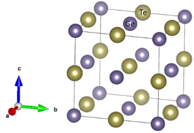
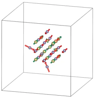
Figure 3.1: The conventional cell of cubic rocksalt structure β-GeTe (F m¯3m group), where the purple balls are Ge atoms, and the yellow balls are Te atoms.
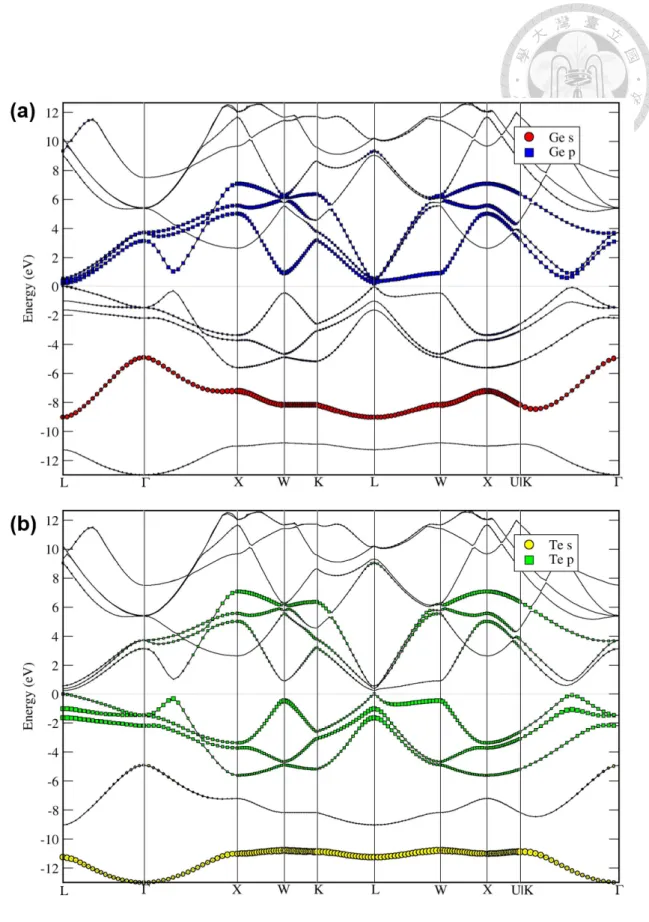
Figure 3.2: The band structure of β-GeTe with projections onto (a) Ge s- and p-orbitals, and (b) Te s- and p-orbitals. The high symmetry points according to which the band structure is drawn are defined in A.1.
doi:10.6342/NTU201701378 Figure 3.3: The density of states (DOS) for β-GeTe, where (a) shows the projections onto
Ge s- and p-orbitals, (b) is the projections on Te s- and p-orbitals. The black curves are the total DOS.
3.2 Electronic structure of β-GeTe
The crystal structure of β-GeTe is illustrated in Fig. 3.1, where the space group sym- metry is F m¯3m. The relaxed lattice parameter (for conventional cell) is 6.01 Å. The band structure is plotted in Fig. 3.2, and the (projected) density of states is plotted in Fig. 3.3.
All of these are consistent with previous work [11,31,38]. Note that in the following anal- yses, we will be particularly interested in the bands right below the valence band maxima (VBM). These bands are associated with the p-orbitals of Te atoms as shown in both the projected band structure plot (Fig. 3.2) and the projected density of states plot (Fig. 3.3).
3.3 Energetics
Using the PC obtained in Sec. 3.2, we construct SCs to evaluate the change in the total energy when defects are inserted. The total energies are calculated after the structures are fully relaxed.
3.3.1 Configuration of a V
Geand a S
SbWe first consider the energy dependence on the distance between VGe and SSb. We calculate the total energy of a 6× 6 × 6 SC containing one VGeand one SSb, where they are arranged as first to fifth nearest neighbors on the Ge-sublattice. The results suggest that VGeand SSbmay not have a preferred configuration. This information helps us organize the calculation carried out in the next subsection.
3.3.2 Formation of defects
Here we investigate the formation energies of the defects. A 4× 4 × 4 SC is adopted, and the total energies of a perfect SC, SC with a single VGe, SC with a single SSb, and SC with a VGe–SSb pair are calculated and listed in Table. 3.1. The total energy of the perfect SC is obtained by scaling directly from the total energy of PC. In the case where VGe–SSbpair is presented, they are arranged as nearest neighbors on the Ge-sublattice for
doi:10.6342/NTU201701378 Table 3.1: Total energies of SC and creation energies of defects (eV).
w/o SSb w/ SSb ∆Esub w/o VGe −509.175 −508.381 0.79
w/ VGe −504.637 −505.269 −0.63
∆Evac 4.54 3.11 —
convenience. ∆Evac is the formation energy of VGe, or, the energy needed to remove a Ge atom and place it at infinity. ∆Esubis the formation energy of SSb, or the substitution energy needed to change a Ge atom into a Sb atom.
Our result shows that it is more likely to form VGein the presence of SSb, since ∆Evac will be reduced by 1.43 eV. Or, we can interpret the data in the way that a Ge atom is inclined to be substituted with a Sb atom when a VGeis nearby, for the substitution energy
∆Esubturns from positive to negative. These evidences indicate that VGeand SSbenhance the presence of each other in GeTe system.
3.3.3 Formation of a S
Sbin V
Ge-rich environment
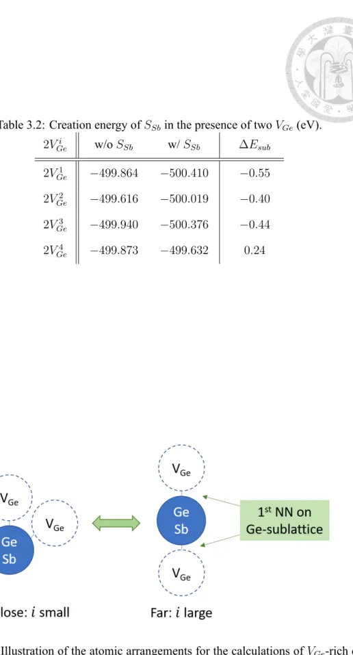
We are interested in the substitution energy ∆Esubin the presence of two VGe. A 4×4×
4 SC containing two VGeis calculated. Note that there are many possible configurations for the two VGe. Here we select a site on Ge-site as the central site, and consider only the cases where both VGe are arranged as nearest neighbors (on the Ge-sublattice) of the central site. Each case is labeled by 2VGei , where a larger i indicates a larger distance between the two VGe. We then compute the total energy for each case with the central site being either Ge or a substituted Sb. The method of configuration is illustrated in Fig. 3.4, and the energies are listed in Table. 3.2.
In general, the result shows that the presence of SSb can decrease the total energy of VGe-rich GeTe system. In other words, although VGeis already a somewhat easily formed intrinsic defect in GeTe, SSbcan further stabilize them and make the system tolerate even more VGe. Note however that the case 2VGe4 shows that the presence of SSb will increase
Table 3.2: Creation energy of SSbin the presence of two VGe(eV).
2VGei w/o SSb w/ SSb ∆Esub 2VGe1 −499.864 −500.410 −0.55 2VGe2 −499.616 −500.019 −0.40 2VGe3 −499.940 −500.376 −0.44 2VGe4 −499.873 −499.632 0.24
Figure 3.4: Illustration of the atomic arrangements for the calculations of VGe-rich envi- ronment. i is the index used in Table. 3.2.
doi:10.6342/NTU201701378 the total energy. Nevertheless, this merely indicates that when there are many VGe, they
will probably favor staying close by rather than on the opposite sides of SSb.
3.3.4 Summary of the energetics
From the results presented in previous sections, we have found that VGeand SSbfacili- tate the formation of each other in the GeTe system based on an energy point of view. This addresses the question why GST compounds are often reported with large concentration of VGe[18, 28, 45, 48].
3.4 Structural relaxation
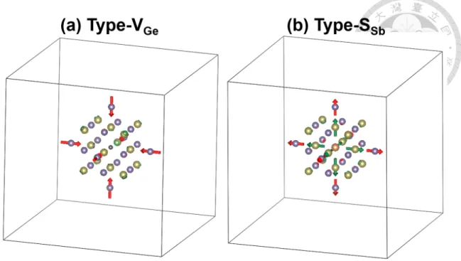
Here we investigate the crystal structure relaxation induced by inserting defects. A 4× 4 × 4 SC is adopted in the calculation. Similar to Fig. 3.1, for visualization, the purple balls and the yellow balls are used to represent Ge atoms and Te atoms, respectively.
Additionally, VGeare represented by black balls, and SSbare represented by orange balls.
Except for the site at the center, each Ge atom is attached with a red arrow, and each Te atom is attached with a green arrow. The arrows indicate the magnitude and direction of the displacement of each atom after adding the defects. For visual convenience,the scale of the arrow length is different in each figure. To simplify the figures, we will show only the first and second nearest layers of Ge and Te with respect to the defect at the center.
3.4.1 Single defect induced relaxation
Relaxations of two 4× 4 × 4 SCs each containing a VGe(type-VGe) or SSb(type-SSb) are calculated. The results are illustrated in Fig. 3.5.
It is obvious that in both relaxation types, the induced displacement is significant only for the atoms on the Cartesian x-, y-, and z-axis, while it is negligible for other atoms. We thus explicitly extract the data of those atoms, including the first nearest Te layer (denoted by NL1Te) and the second nearest Ge layer (denoted by NL2Ge), into Table. 3.3. The largest induced atomic displacement in the presence of VGeis 0.154 Å, which is consistent to the
Figure 3.5: Structural relaxation of a 4× 4 × 4 SC in the presence of (a) a single VGe
(black ball) at the center, and (b) a single SSb(orange ball) at the center.
result given by Edwards et al. [11]
Table 3.3: Displacement data for the atoms on Cartesian axes in Fig. 3.5.
(a) Type-VGe (b) Type-SSb
NL1Te 0.002 Å outward 0.067 Å outward NL2Ge 0.154 Å inward 0.061 Å outward
For the type-VGerelaxation, it is not surprising that NL2Gewill move inward, since the removal of a Ge atom at the center will release considerable space. However, although being closer to the center, NL1Tebarely move. This may be due to the combination of geo- metric and chemical tendencies. Like NL2Ge, NL1Te also tends to move inward in response to the released space. Nevertheless, due to their anion role in GeTe system, Te atoms tend to grab electrons from Ge atoms. Since a Ge atom is now removed, the surrounding Te atoms move away from the vacancy in order to seek compensation from the Ge atoms on the opposite sides. These two kinds of tendency cancel out, which leads to the steadiness of NL1Te.
doi:10.6342/NTU201701378 stitutional Sb atom (period 4) is bigger in size than the original Ge atom (period 3), NL1Te
is pushed outward, and NL2Ge moves outward as well as a secondary response. The fact that the displacement magnitudes of NL1Te and NL2Ge are nearly the same supports this explanation.
3.4.2 Relaxation induced by the combination of V
Geand S
SbFigure 3.6: Structural relaxation of a 4× 4 × 4 SC in the presence of a VGeand a SSb.
For further verification, we also calculated the relaxation of a 4× 4 × 4 SC containing both a VGe and a SSb as illustrated in Fig. 3.6. The two defects are arranged as nearest neighbors on the Ge-sublattice. The displacement magnitudes of the atoms are confirmed all smaller than 0.2 Å.
3.4.3 Summary of relaxation analysis
It has been shown that the relaxation induced by VGeand SSbin GeTe systems is fairly small. Furthermore, if the defects are disordered as described in Ref. [7, 8, 26–28, 39, 42], the relaxation is likely to average out. Not only does this suggest that doping Sb into GeTe will not change the crystal structure, but it supports the fact that the cubic structure of GST samples can sustain very large concentration of vacancies [18, 28, 45, 48].
Since cubic GST’s crystal structure is not too deviated from the rocksalt structure, we expect its band structure to be similar to that of β-GeTe as well. Note that if we want to make estimate for electronic transport properties, the bands around the Fermi level are specifically important. Because GST are often reported as p-type semiconductors due to the large amount of intrinsic VGe[7, 35, 39, 45], the bands below the VBM are particularly of interest. As mentioned in Sec. 3.2, the GeTe bands below the VBM are contributed by Te-p orbitals. Recall that Te atoms are exceptionally steady in the type-VGe relaxation, therefore the bands contributed by them should remain especially stable going from the β-GeTe to GST. Therefore, using the rigid band model based on the β-GeTe electronic structure in order to estimate cubic GST’s transport properties is expected to be a valid and effective approach.
3.5 Unfolded band structures
In this section, we investigate explicitly how the band structure is going to be affected by various concentrations of defects. SC with various sizes are constructed and inserted with a few defects. After being fully relaxed, their unfolded band structures are then obtained by using the B UP [29] code. As for band structure plots, the PC k-path along which the unfolded bands are drawn is identical to the one used in Fig. 3.2, and the Fermi level in each graph is set to be zero.
3.5.1 Electron counting
Some prior knowledge regarding the relation between the composition, number of electrons, and electronic states could be helpful for understanding the position of the Fermi levels in the figures that we are going to discuss.
To begin with, any SC that we calculate corresponds to a normalized chemical formula:
Ge(1−CV−CS)Sb(CS)Te, (3.1)
doi:10.6342/NTU201701378 to the valence electrons of each atom given in A.2, the normalized total number of valence
electrons used in the DFT calculation is equal to
N = 10− 4CV+ 1CS. (3.2)
Also, we have found that regardless of which SC we use, the integrated number of states at VBM will always follow
IDOS
VBM = 10− 2CV. (3.3)
Eq. 3.3 suggests that the states below VBM is independent of the presence of SSb. This is not surprising, since the states below VBM originally provided by Ge atoms can be fully compensated by the states of Sb atoms.
Using Eq. 3.1, 3.2, and 3.3, we can thus have a sense of the position of the Fermi level of each SC.
3.5.2 Band structure with defects
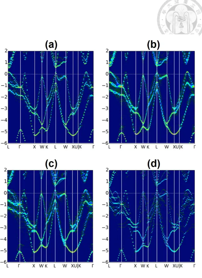
Here we consider the unfolded bands from SC calculations with different sizes where each contains one VGeor one SSb. The SC used and their corresponding normalized chem- ical formula and defect concentrations are listed in A.3. The smaller the SC is, the larger the defect concentration it has.
The result for the SC containing one VGeis shown in Fig. 3.7. As described by Eq. 3.3 and 3.2, we simultaneously lose 4 electrons and 1 state below VBM whenever a VGe is formed. Since the loss of state cannot compensate the loss of electrons, the Fermi level is lowered into the valence band. On the other hand, the result for the SC containing SSbis given in Fig. 3.8. On the contrary, in these cases the Fermi level moves into the conduction band due to the extra electrons provided by Sb. Clearly, for all the cases considered above, the region near the VBM barely reveals new features, and the overall dispersions remain very similar to the β-GeTe band structure up to 12 at.% of defect.
Figure 3.7: Unfolded bands for (a) 3×3×3 SC (b) 2×3×3 SC (c) 2×2×3 SC (d) 2×2×2 SC, each containing one VGe.
doi:10.6342/NTU201701378 Figure 3.8: Unfolded bands for (a) 3×3×3 SC (b) 2×3×3 SC (c) 2×2×3 SC (d) 2×2×2
SC, each containing one SSb.
3.5.3 Band structure with both V
Geand S
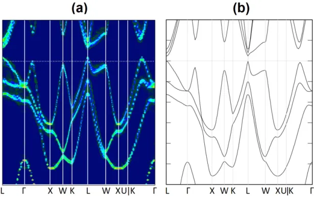
SbFor further confirmation, we investigate the combined influence by both types of de- fects on the band structure. Note that in Ref. [45], the unfolded band structure of a 4×4×4 SC containing a VGe and a SSb, arranged as first nearest neighbors on the Ge-sublattice, is already shown very similar to the β-GeTe band structure. Here, we want to consider a SC containing two VGeand one SSb, which was previously discussed in Sec. 3.3.3. Since 2VGe1 is shown to have the lowest total energy among all possible configurations listed in Table 3.2, it is chosen as our SC here. The unfolded bands of 2VGe1 is shown in Fig. 3.9(a).
Figure 3.9: (a) Unfolded bands of the 2VGe1 SC from Table 3.2. (b) Zoom-in band structure of β-GeTe for comparison.
In this case, the defect concentration is 4.7at.% (3.1 at.% of VGe, 1.6 at.% of SSb).
It is obvious from Eq. 3.2 and 3.3 that in this configuration, the system exhibits a p-type behavior with its Fermi level below the VBM. The dispersions are again very similar to those of β-GeTe. Although there are some splittings near−5 eV, they are too deep and is irrelevant to transport properties. However, it is noteworthy that there is also a minor splitting of about 0.3 eV at the W-point near−0.5 eV. This splitting gives an estimate of
doi:10.6342/NTU201701378 the error bar that we may have if we are to calculate the transport properties of cubic GST
using β-GeTe band structure.
3.5.4 Quantitative measure of band rigidity
To obtain a quantitative measure of the rigidities of SC electronic structures, we com- pute the “root-mean-square deviation (RMSD) per energy eigenvalue” of the unfolded spectra by comparing them to the PC spectrum. In order to do this, a Γ-centered 4× 4 × 4 Monkhorst-Pack k-mesh is adopted to calculate the PC spectrum, and the SC electronic structures are unfolded onto this k-mesh, subsequently. Here, only the states below the VBM are considered. And for the purpose of reducing numerical noise, in each unfolded spectra, the spectral points with intensities smaller than 9% of the maximum intensity are dropped. Then, using the bottom of valence band as the reference point for alignments, we assign each of the remainder spectral peaks to its closest energy eigenvalue in PC spectrum and calculate the distance between them. Lastly, with proper weighting and av- eraging, we derive the RMSD per energy eigenvalue for each SC’s unfolded spectrum.
From the fact that the bottom s-bands, as shown in Fig. 3.2, are irrelevant to the transport properties and are completely separated from other bands, we also compute the RMSD per energy eigenvalue solely for the p-bands near the VBM by excluding the contribution by the s-bands. Since Fig. 3.7(d), 3.8(d), and 3.9(a) are the most representative unfolded band structures for they have the largest concentration of defects or show the combined influence by both types of defects, we only calculate the RMSD per energy eigenvalue for the SCs corresponding to these figures. The results for the three unfolded spectra are listed in Table. 3.4. As we can see, the deviation per energy eigenvalue, which gives an estimate of the error bar that we may have when calculating transport properties, is less than a small value of 0.2 eV.
3.5.5 Summary of unfolded bands
It has been explicitly shown that the band structure of β-GeTe is barely affected by the presence of either VGe, SSb, or a combination of them up to large concentrations. This
Table 3.4: Root-mean-square deviation per energy eigenvalue for the unfolded spectra.
The unit is in eV.
s-bands
Corresponding supercell included excluded Fig. 3.7(d) 2× 2 × 2 w/ 1VGe 0.187 0.175 Fig. 3.8(d) 2× 2 × 2 w/ 1SSb 0.111 0.081 Fig. 3.9(a) 4× 4 × 4 w/ 2VGe& 1SSb 0.108 0.118
agrees with the prediction from the structural analyses in Sec. 3.4.
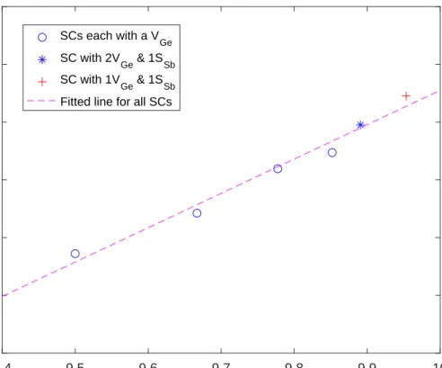
Moreover, if we set VBM as reference point (E = 0), the Fermi level and the number of electrons per normalized chemical formula (Eq. 3.2) of each SC will strictly follow a linear relation, as shown in Fig. 3.10.
9.4 9.5 9.6 9.7 9.8 9.9 10
Number of electrons per normalized chemical formula -0.6
-0.5 -0.4 -0.3 -0.2 -0.1 0
Fermi level (eV)
SCs each with a V
Ge
SC with 2V
Ge & 1S
Sb
SC with 1V
Ge & 1S
Sb
Fitted line for all SCs
Figure 3.10: Fermi level versus number of electrons per chemical formula of each SC.
These evidences suggest that the effect of adding VGe and SSb into GST system is actually just tuning the Fermi level of the system. Therefore, the validity of the rigid band
doi:10.6342/NTU201701378 is again verified.
3.6 Boltzmann theory calculations and direct comparison to experiment data
In the previous sections, the rigid band model approach of using the β-GeTe electronic structure to estimate cubic GST’s transport properties has been shown to be promising.
In this section, we test the applicability of the approach by directly comparing the ex- perimentally measured transport data to our Boltzmann theory calculations done by the B T P [25] code.
Since the GST thin films reported by Wong et al. [45] possess so far the best thermo- electric performance, we choose them as our subject of comparison.
3.6.1 Experimental results by Wong et al. [45]
We now introduce some information regarding the GST thin films that we will make comparisons with. They are prepared on Si substrates, and are shown to be in the F m¯3m cubic rocksalt phase throughout the operating temperature range of 25–300◦C. They are reported with an extreme stoichiometry of Ge0.566Sb0.171Te with up to 25 at.% vacancies, which can be explained by our energetics calculations in Sec. 3.3 and structural relaxation calculations in Sec. 3.4. Using the VBM as the reference point (E = 0), ultraviolet pho- toelectron spectroscopy (UPS) data show that their Fermi level decreases from−0.24 to
−0.52 eV with respect to the increase in temperature. Accordingly, we begin our calcula- tion by scanning the Fermi level from−0.1 eV to −0.5 eV on the β-GeTe band structure with an energy step of 0.1 eV. The positions of the scanned levels are illustrated in A.4.
For more details regarding the GST thin films, one can refer to Ref. [45].
3.6.2 Seebeck coefficient
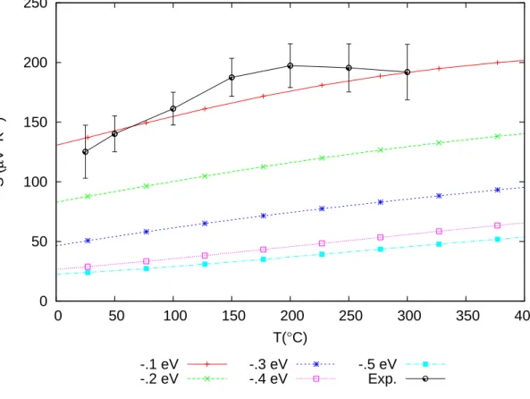
As explained in Section 2.3, Seebeck coefficients are quantities that can be calculated without ambiguity in Boltzmann theory under the constant relaxation time approxima- tion. The comparison of the computed and the measured Seebeck coefficient is shown in Fig. 3.11. Clearly, the Fermi level at−0.1 eV gives a very accurate estimation.
0 50 100 150 200 250
0 50 100 150 200 250 300 350 400
S (µV·K-1 )
T(°C) -.1 eV
-.2 eV
-.3 eV -.4 eV
-.5 eV Exp.
Figure 3.11: Seebeck coefficient as a function of temperature. “Exp.” is the measured Seebeck coefficient of the GST thin flims provided by Wong et al. [45]
3.6.3 Carrier concentration
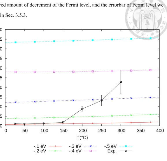
Carrier concentration is another quantity that can be obtained without ambiguity. The comparison of the computed and the measured carrier concentration is shown in Fig. 3.11.
The experimental result of the carrier concentration shows a significant increase with tem- perature. Wong et al. attribute this to the decrease of Fermi level into deeper bands [45].
Here, by directly comparing the computed curves and the measured curve, it is shown that
doi:10.6342/NTU201701378 the observed amount of decrement of the Fermi level, and the errorbar of Fermi level we
predicted in Sec. 3.5.3.
0 5 10 15 20 25 30 35 40 45 50
0 50 100 150 200 250 300 350 400
N (×1020 cm-3 )
T(°C) -.1 eV
-.2 eV
-.3 eV -.4 eV
-.5 eV Exp.
Figure 3.12: Carrier concentration versus temperature. “Exp.” is the measured carrier concentration of the GST thin flims provided by Wong et al. [45]
3.6.4 Relaxation time
As described in Sec. 2.3, under the constant relaxation time approximation for Boltz- mann theory, electrical conductivity and electronic thermal conductivity are inevitably derived with an relaxation time factor. This forbids us from directly comparing the com- puted data to the experimental data. However, we can estimate the relaxation time twice by comparing both the computed electrical conductivity and electronic thermal conductivity to the experiment results, and check if the two values derived individually are consistent.
The calculated electrical conductivity over the relaxation time (σ/τ ) and the mea- sured electrical conductivity of the GST thin films are plotted in Fig. 3.13. As shown in the figure, the observed electrical conductivity is ~105 Ω−1m−1. If we believe that the
0 1e+20 2e+20 3e+20 4e+20 5e+20 6e+20
0 50 100 150 200 250 300 350 400 0 500 1000 1500 2000 2500
σ/τ(Ω-1 m-1 s-1 ) σExp.(Ω-1 cm-1 )
T(°C) -.1 eV
-.2 eV
-.3 eV -.4 eV
-.5 eV σExp.
Figure 3.13: The curves labelled with “eV” are the calculated electrical conductivity over relaxation time (σ/τ ). “σExp.” is the data of the measured electrical conductivity of the GST films provided by Wong et al. [45]
Fermi level really does lie in the range in which we do the calculation (−0.1 to −0.5 eV), the computed σ/τ is ~1020 Ω−1m−1s−1. This means that the relaxation time should be
~10−15s.
The calculated electronic thermal conductivity over the relaxation time (κele/τ ) and the measured total thermal conductivity of the GST thin films are plotted in Fig. 3.14.
The computed κele/τ is ~1015W−1m−1K−1s−1, the observed total thermal conductivity is ~100 W−1m−1K−1. Here we cannot extract the electronic contribution to the total thermal conductivity. However, if we assume that the electronic thermal conductivity is approximately of the same order of magnitude of the total thermal conductivity, then the relaxation time should be ~10−15s, which is consistent with the estimation from electrical conductivity comparison.
doi:10.6342/NTU201701378 0
1e+15 2e+15 3e+15 4e+15 5e+15 6e+15 7e+15 8e+15 9e+15 1e+16
0 50 100 150 200 250 300 350 400 0 0.5 1 1.5 2
κele/τ (W·m-1 K-1 s-1 ) κtot,Exp.(Ω-1 m-1 K-1 )
T(°C) -.1 eV
-.2 eV
-.3 eV -.4 eV
-.5 eV κtot,Exp.
Figure 3.14: The curves labelled with “eV” are the computed electronic thermal conduc- tivity over relaxation time (κele/τ ). “κtot,Exp.” is the data of the measured total conductivity of the GST films provided by Wong et al. [45].
3.6.5 Summary of transport calculations and speculation on the sub- strate
We have demonstrated that by using the β-GeTe band structure, we can make rea- sonable estimates of the transport properties of the cubic GST systems. Furthermore, by comparing to the experimental transport data, our rigid band model predicts a Fermi level of the GST thin films to lie between −0.1 to −0.5 eV below VBM, which is in good agreement with−0.24 to −0.52 eV observed by the UPS measurement [45].
However, using Eq. 3.2 and the composition mentioned in Sec. 3.6.1, the number of electrons per normalized chemical formula of the GST thin films should be 9.12. If the linear relation between the number of electrons and the depth of chemical potential in Fig. 3.10 is correct, then the GST thin films should have their Fermi level much lower than−0.5 eV, which disagrees with both the experiment measurement and our calculation.
Thus, there must be some source that provides extra electrons to the GST thin films so that the Fermi level is pushed to the observed position. We speculate that it is the substrate that is responsible for such compensation. In other words, when it comes to the preparation of GST thin films, substrates may contribute a decisive influence, through the Fermi level tuning, on the transport properties of the films.
3.7 Conclusion
In this work, we have studied the cubic GST systems by comparing them to β-GeTe.
Our energetics calculations showed that the Ge vacancies and Sb substitution facilitate the presence of each other in β-GeTe system, which explains the often reported extreme stoichiometries of cubic GST compounds. By investigating the deformation of the crystal structure and the band structure, we showed that the Ge vacancies and Sb substitutions barely perturb the cubic GST systems from β-GeTe characteristics. This indicates that the function of them is merely tunning the Fermi level. Based on these facts, we proposed a rigid band model of using the β-GeTe band structure to estimate the transport properties of cubic GST systems. By directly comparing with the experiment results of the GST thin films reported by Wong et al. [45], we demonstrated the accuracy and usefulness of the rigid band model. Additionally, we speculate that the substrate play an decisive role in the transport properties of cubic GST thin films.
GST is a very promising type of thermoelectric material because of its superior and tunable thermoelectric properties. We believe that our work will serve as a guideline that expedites the understanding, design, and engineering processes of GST for thermoelectric applications.