Effect of Thermal Annealing on Ga-Doped ZnO Films
Prepared by Magnetron Sputtering
J. K. Sheu,a,zK. W. Shu,aM. L. Lee,bC. J. Tun,cand G. C. Chic a
Institute of Electro-optical Science and Engineering, National Cheng Kung University, Tainan 70101, Taiwan
b
Department of Electro-optical Engineering, Southern Taiwan University, Yung-Kang City,Tainan 710, Taiwan
c
Department of Physics and Optical Science Center, National Central University, Jhongli 32001, Taiwan
In this study, Ga-doped ZnO共GZO兲 films deposited on a sapphire utilizing magnetron cosputtering method using ZnO and Ga2O3
targets were demonstrated. The results revealed that the resistivities of the GZO films reduced by at least two orders of magnitude after the thermal annealing. The reduction in resistivity could be attributed not only to the activation of Ga dopants and to the increase of electron mobility, but also to the enlargement of the grain size that occurred as a result of thermal annealing. The resistivity of GZO films reduced from 1.4⫻ 10−1to 5.3⫻ 10−4⍀ cm after the films had undergone thermal annealing in nitrogen
ambience with temperature ranging from 400 to 800°C. Additionally, the GZO films exhibited semiconducting conductivity and metallic conductivity in as-deposited and annealed samples共⬎600°C兲, respectively.
© 2007 The Electrochemical Society. 关DOI: 10.1149/1.2721760兴 All rights reserved.
Manuscript submitted August 30, 2006; revised manuscript received January 29, 2007. Available electronically April 13, 2007.
Some optoelectronic devices such as flat panel displays, solar cells, and light-emitting diodes 共LEDs兲 require transparent elec-trodes to be used as the top contact layers. Transparent elecelec-trodes consist of low-resistivity transparent conducting oxides共TCO兲 and thin metal. Although indium tin oxide共ITO兲 thin films have been widely used in most practical applications of transparent electrodes, there are many reports demonstrating other areas of applications for TCO that include a range of deposition methods.1Recent research efforts have focused on the application of ZnO-based thin films as transparent electrodes. The transparent electrodes have been a sub-ject of extensive study because they exhibit great resource availabil-ity, nontoxicavailabil-ity, and high thermal and chemical stability. Although undoped ZnO films prepared by radio-frequency 共rf兲 magnetron sputtering demonstrate low resistivity of around 4.5⫻ 10−4⍀ cm,2 the films were found to be unstable at temperature levels exceeding 150°C.3The use of impurity-doped ZnO thin films1is considered as a suitable alternative to ITO, in particular for special applications. The doped ZnO films are viewed as a preferable alternative due to their very high stability. In the 1980s, transparent conducting ZnO films with resistivities equal to 104⍀ cm were prepared by impurity doping with a group III element4,5such as Al, Ga, In, and B. To be used as electrodes in LEDs, the resistivity of ZnO-based thin films must exhibit high thermal stability. High thermal stability is a nec-essary condition because most device process procedures consist of a series of heat-treatments with temperature levels reaching above 500°C. High-temperature treatments are the prerequisite when the films are intended to serve as transparent contact layers of GaN-based LEDs.6-9Furthermore, long-term reliability of the fabri-cated devices, featuring TCO that are used as electrodes, strongly depends on the stability of TCO films.
In this study, the Ga-doped ZnO共GZO兲 thin films were deposited on a sapphire substrate using magnetron sputtering method. ZnO and Ga2O3 targets were used as the sputtering sources during cosputtering deposition. The sputtering method in our experiment was different from the conventional process using a mixed target with fixed Ga2O3content serving as the source in magnetron sput-tering or pulsed laser deposition method.4,10-14Due to the difference in the sputtering method, one must prepare several mixed targets with different Ga2O3content to adjust the Ga doping level in GZO films. In this study, the cosputtering process offered flexibility in selecting the doping amount of Ga atoms by changing the sputtering power of ZnO and Ga2O3targets. Additionally, experimental results
showed that electrical resistivity and optical transparency of GZO films could be improved further by thermal annealing in nitrogen ambience.
Experimental
All films used in this study were deposited on c-face sapphire-共0001兲 substrates using magnetron sputtering method. Note that the substrate temperature during the deposition was well below 50°C. The GZO films were prepared by cosputtering of ZnO and Ga2O3 targets with purity of 99.99%. The cosputtering process was con-ducted in argon gas under a pressure of 1⫻ 10−2Torr. DC and rf powers were used for ZnO and Ga2O3targets, respectively. In this study, the dc power was fixed at 200 W for ZnO target. On the other hand, different rf powers共50, 100, and 200 W兲 were employed for Ga2O3target to produce GZO films with different Ga doping levels. Ga contents in the resulting GZO films were estimated to be around 0.5, 2.9, and 8%, for 50, 100, and 200 W rf power levels, respec-tively: The results above were obtained using X-ray photoelectron spectroscopy 共XPS兲 analysis. Note that the determination of Ga composition in GZO films was based on a calibrated standard sample. For comparison purposes, undoped ZnO films were also prepared using dc sputtering with power level equal to 200 W. The thickness of the GZO and the ZnO films was kept at 250 nm, as determined by variable angle spectroscopic ellipsometry. Deposited GZO and ZnO films were then thermally annealed for 1 min in nitrogen ambience at different temperatures ranging from 400 to 800°C. Electrical resistivity and electron mobility of the GZO and ZnO films were measured by van der Pauw technique共BIO-RAD HL5500 Hall measurement system兲 at different temperatures. Note that the as-deposited ZnO films exhibited highly resistive properties, with a sheet resistivity higher than 109⍀ cm, thus exceeding mea-surement limitations of our instruments. However, electrical proper-ties of ZnO films could be significantly improved after thermal an-nealing process at a temperature above 400°C. The crystallinity of the ZnO-based films was investigated using X-ray diffraction共XRD兲 with a conventional X-ray unit and a copper anode共BEDE Dl sys-tem兲. The transmission spectroscopy was measured using a Perkin Elmer Lambda 40 spectrometer.
Results and Discussion
It has been tentatively proposed that electron concentration in sputtered ZnO thin films could be attributed to the oxygen vacancy 共VO兲 and the Zn interstitial sites 共Zni兲.1-5,15,16Figure 1a shows
elec-tron concentration and resistivity of the ZnO films used in this study. Both as-deposited and 400°C annealed ZnO films showed highly resistive properties, which could be attributed to the hindered carrier z
E-mail: [email protected]
Journal of The Electrochemical Society, 154共6兲 H521-H524 共2007兲
0013-4651/2007/154共6兲/H521/4/$20.00 © The Electrochemical Society H521
transport across the grain barriers and deficiency of carrier density. Increased resistivity could also be attributed to lattice defect-induced trapping states occurring at grain boundaries. Defect-induced trap-ping states take place to compensate a fraction of carriers and/or result in a potential barrier across the depletion region. Conse-quently, the potential barrier will hinder the carrier transport from one grain to another.17 However, decreased resistivity observed in the annealed ZnO films can be attributed to the fact that crystallite size becomes larger. As a result, the defect induced trapping states occurring at grain boundaries to compensate the carriers will be
alleviated due to the enlargement of crystallite size.17We also ob-served an increase in electron concentration that took place along with the increase in annealing temperature, as shown in Fig. 1a. Furthermore, electron mobility also increased along with the anneal-ing temperature, as shown in Fig. 1b. Increase in mobility could occur due to the reduction of grain boundary scattering for electron transport.13 On the other hand, the highly resistive properties of undoped ZnO could be altered drastically by adding a number of group III impurities.1 As shown in Fig. 1c, the resistivity of as-deposited GZO films decreased when the rf powers applied to Ga2O3targets were increased. In other words, the incorporated Ga amount in the resistivity of GZO films increases along with rf pow-ers applied to Ga2O3target, thus resulting in a reduction in resistiv-ity. For example, as-deposited GZO films showed typical resistivity as low as 2.3⫻ 10−2⍀ cm when an rf power of 200 W was applied to the Ga2O3target during the deposition of GZO films. Applied rf power of 200 W corresponded to a Ga content of around 8%. Al-though the resistivity of the as-deposited GZO films was much lower than that of as-deposited ZnO films, it was still insufficiently low to serve as an electrode material. To further reduce the resistiv-ity of GZO films, all samples were annealed in N2 ambience at different temperatures. As shown in Fig. 1c, the resistivity of GZO films could be significantly reduced to as low as⬃10−4⍀ cm when the annealing temperatures exceeded 600°C. For typical TCO films, the resistivity was proportional to the reciprocal of the product of carrier concentration and mobility. Therefore, a decrease in resistiv-ity taking place along with the increase of annealing temperature could be attributed to the increase in mobility and the carrier con-centration, thus reflecting film qualities and the activation of dopants 共Ga兲, respectively.
We conducted XPS analysis共data not shown here兲 in an attempt to determine the concentration of VOin ZnO films. The results re-vealed that oxygen percentage in the ZnO-based films remained vir-tually unchanged after thermal annealing. Constant oxygen percent-age may possibly be explained by inefficient resolution of XPS. Therefore, in this case, we could not conclude whether increased electron concentration resulted in increase of VO or not. For in-stance, GZO films with Ga content of 2.9%共i.e., instance where rf power of 100 W was applied to Ga2O3 target兲, had resistivity that was reduced by at least two orders of magnitude when thermal an-nealing temperature was increased above 600°C, as shown in Fig. 1c. However, the difference in electron concentration between as-deposited films and GZO films annealed at 600, 700, and 800°C was about one order of magnitude. Our results indicate that reduction in resistivity also comes from increase in electron mobility in addition to the increase of electron concentration. The latter could be attrib-uted to the increase of Ga activation efficiency. This phenomenon is consistent with previous reports.13,14,19,21
According to the results of the Hall-effect measurements, elec-tron mobility of the annealed GZO films increased along with the increase of annealing temperatures, as shown in Fig. 1b. Thus, the increase in electron mobility should be taken into account when we analyze the decrease in resistivity of the annealed GZO films. The improvement in electron mobility could be attributed to the recrys-tallization of GZO films that takes place during the annealing pro-cess. Consequently, recrystallization results in reduction of electron scattering probability at grain boundaries.17,19,21 In other words, small crystallites coalesce to form larger crystallites during the an-nealing process.18To clarify our assumptions, XRD analyses were performed on the annealed GZO films with Ga content of 2.9%. Note that only one peak corresponding to the 共0002兲 plane was observed in the GZO films. The presence of one peak indicates that the GZO films exhibited strong c-axis orientation. In addition, the diffraction angle of GZO films increased from 2 = 34.16° to 2 = 34.46° when annealing temperature was increased from 400 to 800°C 共see Fig. 2兲. The diffraction angles were lower than the 34.47° angle observed for ZnO bulk material. Lower diffraction angles imply that the interplanar spaces of the GZO thin films were larger than those in ZnO bulk material. Hence, larger interplanar
Figure 1.共a兲 Resistivity and electron concentration of ZnO films as a
func-tion of annealing temperature.共b兲 Electron mobility of GZO and ZnO films as a function of annealing temperature.共c兲 Resistivity and electron concen-tration of GZO films as a function of annealing temperature.
H522 Journal of The Electrochemical Society, 154共6兲 H521-H524 共2007兲 H522
spaces could be attributed to the crystalline imperfections such as lattice strain and interstitial defects.18At the same time, the diffrac-tion angles of the annealed GZO films shifted toward the high-angle side by 0.3°, indicating that compressive strain components共parallel to c-faces兲 in the as-deposited samples could be relaxed using the thermal annealing process. Similar results were also observed in the ZnO thin films.18-20As shown in Fig. 2, the full width at half maxi-mum共fwhm兲 of XRD 共0002兲 peak decreases with an increase of annealing temperature, indicating that crystal quality of the GZO films could be improved by thermal annealing. The results of the XRD analysis were also consistent with the results of Hall measure-ments. Both XRD and Hall measurements suggest that improvement in electron mobility of the annealed GZO and ZnO films occur due to the recrystallization of GZO. The reduction of XRD fwhm origi-nates from the formation of larger crystallites during annealing pro-cess and thereby results in reduction of electron scattering probabil-ity.
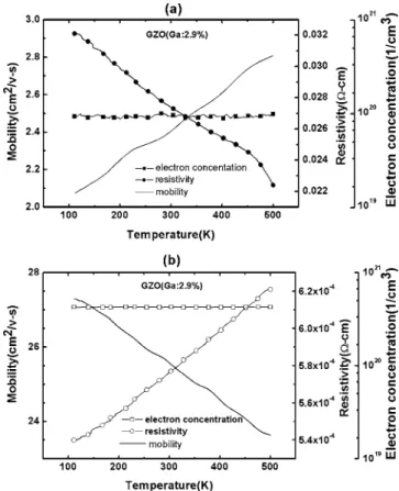
To further clarify the role of mobility and electron concentration in reduction of resistivity for as-deposited and annealed GZO films, we performed temperature-dependent Hall-effect measurements on the GZO films. Previous reports suggest that when measuring tem-perature is less than 130 K, electrical properties such as resistivity, carrier concentration, and mobility of Ga-doped ZnO films remain virtually unchanged. However, electrical properties of sputterd ZnO films change along with fluctuation of temperature above 130 K.21 In this study, the temperature-dependent Hall measurements were performed at temperatures ranging from 100 to 500 K. Figure 3a shows a typical result of temperature-dependent Hall measurement of as-deposited GZO films with Ga content of 2.9%. The resistivity decreases with an increase in temperature in the range of 100 to 500 K. Experimental observations suggest that the as-deposited GZO films with medium carrier concentration of around⬃1019/cm3 appear due to a combined effect of Ga doping and/or VOand Zni. On the other hand, the carrier concentration exhibits nearly temperature-independent behavior indicating that the as-deposited GZO films are degenerate semiconductors. Therefore, the resistivity with semicon-ducting properties in the as-deposited GZO films can be attributed to the increase in electron mobility under high-temperature conditions. The aforementioned observations imply that the electron scattering mechanism is dominated by grain boundary scattering due to small grain size in as-deposited GZO films.21In other words, the potential barrier between grain boundaries is high enough to lead to the phe-nomenon known as thermally activated mobility. However, after the GZO films were annealed at a given temperature 共700°C兲 men-tioned above, the Ga dopants were found to play an important role in increasing carrier concentration and hence reducing resistivity.
Annealed GZO films with carrier concentration of around ⬃1020cm−3, which is five times the magnitude of as-deposited samples, can be explained by the increase in activation efficiency of Ga dopants present in ZnO. The room-temperature electron mobility of annealed GZO films was around 25 cm2/v-s, which is one order of magnitude higher than the mobility of as-deposited samples. Higher mobility in annealed GZO films could be attributed to the coalescence of small grains and consequently reduced electron scat-tering at grain boundary. When we look at the 700°C annealed samples, the carrier concentration of the samples also shows a nearly temperature-independent behavior. Such behavior indicates that 700°C annealed samples are also degenerate semiconductors, as shown in Fig. 3b. In addition, one can see that the resistivity of 700°C annealed GZO films increases with temperature. Such behav-ior implies that the 700°C annealed GZO films have metallic con-ducting property which can be explained by the formation of a de-generate band appearing in heavy doped semiconductors, as suggested by Mott.22Positive coefficient of resistivity has been re-ported in the highly conductive Al-doped ZnO23 and Nb-doped TiO2,24which could be attributed to the fact that Hall mobility de-creased along with an increase in temperature, as shown in Fig. 3b. This phenomenon took place due to thermal lattice vibration scat-tering. Thus, the resistivity of 700°C annealed GZO films increased with increase in temperature because the carrier concentration of 700°C annealed samples remained unchanged while the mobility decreased along with increase in temperature.
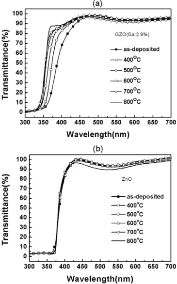
In this study, transmission spectra were also performed to deter-mine optical transmittance of the GZO and the ZnO films annealed at different temperatures. All films exhibited high transmittance in visible region over 90%. The films displayed a sharp fundamental absorption edge at around 380 nm. As shown in Fig. 4a, the absorp-tion band edge tends to shift to a shorter wavelength as the anneal-ing temperature is increased for GZO films. Blue shift is an indicator
Figure 2.共0002兲 XRD spectra and fwhm of GZO films 共with Ga content of
2.9%兲 annealed at different temperatures.
Figure 3. Typical results of temperature-dependent Hall-effect measurement
of共a兲 as-deposited and 共b兲 700°C annealed GZO films 共with Ga content of 2.9%兲.
H523 Journal of The Electrochemical Society, 154共6兲 H521-H524 共2007兲 H523
of a well-known Burstein-Moss 共BM兲 effect.25 Optical bandgaps 共Eg兲 of the GZO films were estimated by extrapolation of the linear portion of square of the absorption coefficient against photon energy 共h兲.26,27As shown in Fig. 4b, the absorption band edge of ZnO films does not shift to a shorter wavelength when the annealing temperature is increased. The optical bandgaps of ZnO films are almost identical falling within the range of 3.31–3.32 eV. In the case of the annealed GZO films, the optical bandgaps increased from 3.59 to 3.71 eV as the annealing temperature was increased from 400 to 800°C. The BM effect occurs when the Fermi level enters into the conduction band. For ZnO films, the Fermi level enters into the conduction band when the donor concentration is larger than 7⫻ 1019cm−3.28
As shown in Fig. 1a. electron concen-tration of the undoped ZnO films, used in this study, is smaller than the specified value of 7⫻ 1019cm−3, even after high-temperature annealing was performed. Thus, no bandgap widening can be ob-served for the annealed ZnO films. However, the carrier concentra-tion of the annealed GZO films increased significantly with increase of the annealing temperature. The carrier concentration of the an-nealed GZO films was well above 1⫻ 1020cm−3with the exception of the GZO films with Ga content of 0.5%, as shown in Fig. 1c.
Therefore, one can tentatively conclude that BM effect can be con-sidered as one of the possible causes of bandgap widening in the annealed GZO films.
Conclusion
We have demonstrated that Ga-doped ZnO共GZO兲 films deposited on a sapphire utilizing magnetron cosputtering method using ZnO and Ga2O3targets could have low resistivity and high transparency. According to the results of our experiments, post-deposition anneal-ing can significantly improve crystal quality of GZO and ZnO films. Both as-deposited and annealed GZO films exhibited high transmit-tance共⬎90%兲 in the wavelength range of 400 to 700 nm. On the other hand, we noted a decrease in the resistivity of GZO films, which occurred due to the activation of Ga dopants. We believe that resistivity decrease also takes place due to the increase in electron mobility, which can be attributed to the enlarged grain size after thermal annealing. Apart from the undoped samples 共ZnO films兲, significant blueshift was also observed in transmission spectra of the annealed films. The origin of the blueshift is explained by the Burstein-Moss effect.
Acknowledgments
The authors thank the Center for Micro/Nano Technology Re-search, National Cheng Kung University, Tainan, Taiwan, for pro-viding equipment. We also acknowledge technical and financial sup-port offered by the National Science Council under contract no. NSC 2221-E-006-416, NSC 2221-E-006-354, and NSC 95-2221-E-218-051.
National Cheng-Kung University assisted in meeting the publication costs of this article.
References
1. T. Minami, Mater. Res. Soc. Symp. Proc., 25, 38共2000兲, and references therein. 2. T. Minami, H. Nanto, and S. Takata, Appl. Phys. Lett., 41, 958共1982兲. 3. T. Minami, H. Nanto, S. Shooji, and S. Takata, Thin Solid Films, 111, 167共1984兲. 4. T. Minami, H. Nanto, S. Shooji, and S. Takata, Jpn. J. Appl. Phys., Part 1, 24,
L781共1985兲.
5. T. Minami, H. Nanto, and S. Takata, Jpn. J. Appl. Phys., Part 1, 23, L280共1984兲. 6. Y. C. Lin, S. J. Chang, Y. K. Su, T. Y. Tsai, C. S. Chang, S. C. Shei, C. W. Kuo, and
S. C. Chen, Solid-State Electron., 47, 849共2003兲.
7. S. M. Pan, R. C. Tu, Y. M. Fan, R. C. Yeh, and, J. T. Hsu, IEEE Photonics Technol. Lett., 15, 646共2003兲.
8. J. O. Song, K. K. Kim, S. J. Park, and T. Y. Seong, Appl. Phys. Lett., 83, 479 共2003兲.
9. L. Y. Chen, W. H. Chen, J. J. Wang, F. C. N. Hong, and Y. K. Su, Appl. Phys. Lett.,
85, 5628共2004兲.
10. V. Bhosle, A. Tiwari, and J. Narayan, Appl. Phys. Lett., 88, 032106共2006兲. 11. Z. F. Liu, F. K. Shan, J. Y. Sohn, S. C. Kim, G. Y. Kim, Y. X. Li, and Y. S. Yu, J.
Electroceram., 13, 183共2004兲.
12. E. Fortunato, V. Assuncao, A. Goncalves, A. Marques, H. Aguas, L. Pereira, I. Ferreira, P. Vilarinho, and R. Martins, Thin Solid Films, 451-452, 443共2004兲. 13. X. Yu, J. Ma, F. Ji, Y. Wang, X. Zhang, and H. Ma, Thin Solid Films, 483, 296
共2005兲.
14. T.-H. Kim, S.-H. Jeong, I. S. Kim, S. S. Kim, and B.-T. Lee, Semicond. Sci. Technol., 20, L43共2005兲.
15. P. Kasai, Phys. Rev., 130, 989共1963兲.
16. K. Vanheusden, C. H. Seager, W. L. Warren, P. R. Tallant, and J. A. Voigt, Appl. Phys. Lett., 68, 403共1996兲.
17. J. Y. W. Seto, J. Appl. Phys., 46, 5247共1975兲, and references therein. 18. V. Gupta and A. Mansingh, J. Appl. Phys., 80, 1063共1996兲.
19. K.-K. Kim, S. Niki, J.-Y. Oh, J.-O. Song, T.-Y. Seong, S.-J. Park, S. Fujita, and S.-W. Kim, J. Appl. Phys., 97, 066103共2005兲.
20. A. Kuroyanagi, J. Appl. Phys., 66, 5492共1989兲. 21. D. H. Zhang and H. L. Ma, Appl. Phys. A, 62, 487共1996兲.
22. N. F. Mott, Conduction in Non-Crystalline Materials, Clarendon, Oxford共1993兲. 23. R. C. Budhani, P. Pant, R. K. Rakshit, K. Senapati, S. Mandal, N. K. Pandey, and
J. Kumar, J. Phys.: Condens. Matter, 17, 75共2005兲.
24. Y. Furubayashi, T. Hitosugi, Y. Yamamoto, K. Inaba, G. Kinodo, Y. Hirose, T. Shimada, and T. Hasegawa, Appl. Phys. Lett., 86, 252101共2005兲.
25. E. Burstein, Phys. Rev., 93, 632共1954兲; T. S. Moss, Proc. Phys. Soc. London, Sect. B, 67, 775共1954兲.
26. I. Hamberg, C. G. Granqvist, K. F. Berggren, B. E. Sernelius, and L. Engstrom, Phys. Rev. B, 30, 3240共1984兲.
27. I. Hamberg and C. G. Granqvist, J. Appl. Phys., 60, R123共1986兲.
28. T. Makino. Y. Segawa, S. Toshida, A. Tsukazaki. A. Ohtomo, and M. Kawasaki, Appl. Phys. Lett., 85, 759共2004兲.
Figure 4. Typical transmission spectra of共a兲 GZO films 共with Ga content of
2.9%兲 and 共b兲 ZnO films annealed at different temperatures.
H524 Journal of The Electrochemical Society, 154共6兲 H521-H524 共2007兲 H524