Damped Input Filter Design of Matrix Converter
Hongwu She, Student Member, IEEE, Hua Lin, Xingwei Wang, and Limin Yue
Huazhong University of Science and Technology, 1037 Luoyu Road, Wuhan, Hubei Province, China [email protected]
Abstract -- This paper deals with the input filter design of matrix converter. Regard the matrix converter as a buck type PWM rectifier in the input side, the transfer function of input current using LC input filter is deduced. The parameter selection approach for the capacitor and inductor is presented.
It has been verified that when LC circuit is adopted in the input filter, the input current will oscillate near the LC resonant frequency in both steady state and start-up process for the very low damping factor, and then the input current waveforms will be distorted. An improved input filter topology to increase the damping factor is then presented, and the damping resistance parameter selection method of the input filter is presented based on frequency response approach. To avoid the current spike at the start-up process, a start-up circuit is then proposed. The improved input filter has been tested on a 5.5kW matrix converter prototype and good performances are achieved.
Index Terms-- matrix converter, input filter, input power factor, damping factor
I. I
NTRODUCTIONThe input filter is generally needed in matrix converter to smooth the input currents and satisfy the electro-magnetic interference (EMI) requirements. Since the matrix converter can be considered as a current source at the input side, a LC circuit is usually adopted in the input filter [1]. As a buck type converter, a salient advantage of matrix converter is that just small input filter is needed to eliminate the current spikes. Moreover, the adoption of input filter can avoid high frequency interferences on the matrix converter in the power system.
Many researchers have been working on the input filter of rectifiers for decades. Factors that contribute to power system pollution caused by diode rectifiers and some effective mitigating methods have been addressed in IEEE519 document [2]. Non-mandatory allowable level of current and voltage distortion for ensuring good power quality in an industrial plant is part of the IEEE519 document. However, the filters need to comply with IEEE519, either active type or passive type, add cost and occupy space [3]. As the matrix converter is high-frequency power electronics equipment, the harmonic contents in the input current are near the switching frequency, so the input filter design of the matrix converter is relatively easier.
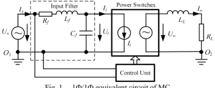
For convenient analysis of the input filter performance, conventional 3Ф/3Ф matrix converter could be equivalent to three 1Ф/1Ф converters in balanced input and balanced load condition. Since the LC circuit is usually adopted in the input filter, the single-phase equivalent circuit of matrix converter is shown in Fig. 1. It can be found from Fig. 1 that the matrix
converter can be considered as a current sink in the input side and a voltage source in the output side.
Fig. 1. 1Ф/1Ф equivalent circuit of MC.
For the past decades, many literatures addressed on input filter design of matrix converter have been published. A two- stage LC filter topology was proposed by in [4] and seems to be a good option of high performance solution. However, by analyzing of the frequency response characteristics, it can be found that the effect of two-stage filter is similar to that of one-stage ones with the same total inductance and capacitance. Moreover, two-stage topology will increase the complexity, reliability and cost of matrix converter. A complicated filter which integrates coupled input and output filters is presented in [5] for low common-mode current, low shaft voltage and sinusoidal output voltage waveforms;
however, this approach leads to a very complex and expensive solution. An input filter design approach based on Pareto optimization was proposed in [6] consider many factors, like construction cost, fundamental frequency phase shift and power dissipation; however, the constraints of these factors were not discussed in the paper.
For the LC filter can be described as a two-order less damping system by transfer function, the input filter is sensitive to input voltage and output current disturbances.
The input current spectrum of matrix converter is obtained by Saber simulation in [7], and then a damped input filter was given; however, the damping circuit design procedure was not presented. It is pointed out in [8] that the damping resister in LC filter can improve the stability of matrix converter;
however, the parameter selection method of damping resistor is also not presented.
This paper deals with the one-stage input LC filter design and optimization of the matrix converter. The single phase equivalent circuit is adopted to analyze the behavior of the input filter. The parameter selection of capacitor and inductor is presented and the transfer function of input current of the input filter is deduced. It can be found that the traditional LC input filter is unstable in steady-state and start-up process for very low damping factor. A topology to improve the damping factor of the filter is presented, and a general design method
PEDS2009
of the damping resistor is presented. The input filter design procedure is applied to a 5.5kW matrix converter and has been verified by simulations and experiments.
II. C
APACITOR ANDI
NDUCTORS
ELECTIONAs a buck type converter, the input current of matrix converter is discontinues, and the input capacitor is necessary to smooth the input current. Unlike boost type rectifiers, the input filter of matrix converter needs relative small inductance and relative large capacitor. In order to get smooth sinusoidal input current, high-quality capacitors with low ESR, ESL and high current rating are required. The existence of capacitor in the input filter will induce capacitive reactive power in the power system, which will lead to low input power factor especially in low power conditions. So the capacitance should be selected upon rated power level. J.
Andreul thinks the power factor should not less than 0.9 in 10% rated power [9]; and C. Klumpner thinks the power factor should not less than 0.85 in this power level [10]; when D. Casadei thinks the power factor should not less than 0.8 in the same condition [11]. The LC filter presented in [12]
exhibits an input power factor of 0.5 in 10% rated power.
YASKAWA said that the input power factor of its matrix converter product is larger than 0.95, although the power condition was not referred [7]. It can be found there are no uniform standard for input power factor in low power conditions. Consider there are generally too much inductance reactive power in low voltage power system, the introduction of capacitance reactive power aroused by the capacitor could improve the power factor of the power network. So the power factor of MC in low power level condition should not be a main constraint of capacitor selection. In order to get better input current waveforms, larger capacitor is appreciated. It seems that the input power factor larger than 0.8 in 10% rated power is a reasonable choice and the range of input filter capacitive power Q
cis presented in (1). The reactive power caused by inductor is ignored in this paper.
2
3
3 10%
c i f n
4
nQ = ω C U ≤ P . (1) The range of capacitor is
40
2 n fi n
C P
ω U
≤ . (2) After the selection of capacitor, the inductor of input filter can be designed to satisfy the standards for harmonic control in power systems. It is also known the design of the input filters is strictly related to the switching frequency and the voltage drop on the inductor should not than 5% of input voltage. Generally, the resonant frequency of the input LC filter is selected to be much higher than the input supply frequency and significantly lower than the PWM switching frequency. Typically, the resonant frequency is higher than 20 times the supply frequency and lower than one-third the PWM frequency [5].
This paper deals with the input filter design of a 5.5kW matrix converter, the system sample frequency is 5k Hz and the power supply is 380V/50Hz. It can be calculated from (2) that the capacitor of input filter should not larger than 9.02μF.
Here, capacitors with 10μF are selected for practical application. The inductance of input filter is 1mH when a resonant frequency of 1.6k Hz is selected.
III. LC F
ILTERC
HARACTERISTICSThe current and voltage relationships in the input filter can be described by transfer functions. As shown in Fig. 1, the L
fand C
fis the inductance and capacitance of the input LC filter, and R
fis the resistance of the inductor. The output current I
iof the LC filter is a series of PWM pulses and the width of the pulses is varying according to sine law. The voltage and current relationships of the input filter are
( ) ( ) ( ) ( )
( ) ( ) ( )
s i f f s
s i f i
U s U s R sL I s I s I s sC U s
− = +
⎧ ⎨ − =
⎩
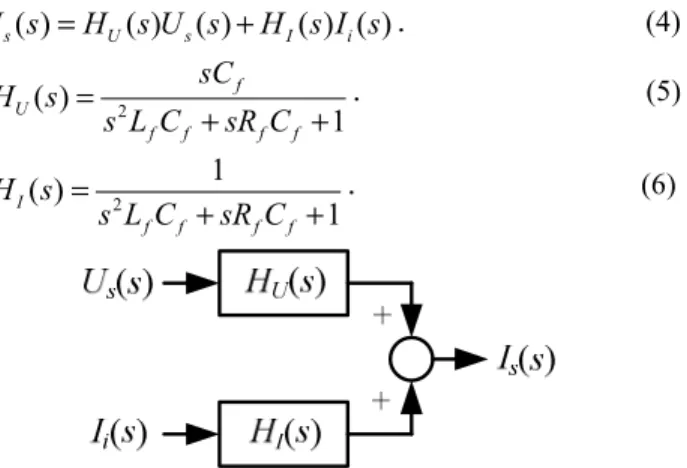
. (3) From (3) the transfer function of input current of input filter can be obtained as shown in (4), where H
U(s) and H
i(s) are shown in (5) and (6). The relationships of the input current I
s, output current I
iand input voltage U
sof the input filter can be described by signal flow diagram as shown in Fig. 2.
( ) ( ) ( ) ( ) ( )
s U s I i
I s = H s U s + H s I s . (4)
( )
21
f U
f f f f
H s sC
s L C sR C
= + + . (5)
2
( ) 1
I
1
f f f f
H s = s L C sR C
+ + . (6)
Fig. 2. Signal flow diagram of the input filter variables.
The H
U(s) is the transfer function related to the input voltage and it’s independent of the output current of the LC filter; when H
i(s) is the transfer function related to the output current and it’s independent of the input voltage. It could be found that the denominator of H
U(s) and H
I(s) is the same and the characteristic frequency ω
nand damping factor ζ of the transfer functions are
n
1/ L C
f fω = . (7)
1 /
2 R
fC
fL
fζ = . (8) Since the resistance of the inductor R
fis usually few milliohms and the value of C
f/L
fis usually less than 1, the damping factor of the input transfer function ζ is usually very small and approaches zero. The output current of the input
PEDS2009
filter I
iis high frequency PWM pulses and it contains plenty of harmonic contents near the switching frequency, which is a strong disturbance on the input filter. This will leads to oscillations of the LC circuit near the resonant frequency.
Resonant frequency harmonic contents will appear in the input current, which will leads to distortion of the input current waveform and instability of the matrix converter.
Although the input voltage also impacts the input current of input filter, the output current factor of the input filter will be solely investigated in this paper. Here, balanced and sinusoidal input voltages are assumed. The input filter of a 5.5kW matrix converter behavior has been investigated by MATLAB/Simulink simulation. The sample frequency of the system is 5k Hz and the detailed parameter of the system is shown in Table I.
TABLEI
MATRIX CONVERTER SIMULATION PARAMETERS Power Supply Input Filter Load
Us=220V (line-to-neutral, RMS),
fi=50Hz
Lf=1mH, Rf=0.01Ω,
Cf=10μF
LL=10mH,RL=22Ω(Y) Uo=185V(RMS), fo=30Hz
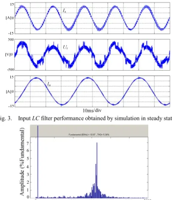
Using the parameter shown in Table 1, the damping factor
ζ of the input filter is 5×10⁻⁴, and the resonant frequency f
ris 1596Hz. The waveforms of output voltage U
i, input current I
sand matrix converter output current I
oget by simulation in steady state are presented in Fig. 3.
Fig. 3. Input LC filter performance obtained by simulation in steady state.
5 6
3
1 0 2 4
0 500 1000 2000 2500 3000
Fudamental (Hz)1500
7
Fig. 4. FFT analysis of LC filter input current waveform in steady state.
It could be noticed from Fig. 3 that there are high order harmonic contents appears on input current waveform, which are mainly because of the low damping factor. The oscillation impacts the waveform of the output voltage of the input filter
and then the output current waveform of matrix converter is also affected. It could be found that the harmonic contents in the input current I
sare near the resonant frequency (1596Hz) of the LC circuit from the FFT analysis presented in Fig. 4.
Start-up is also a strong disturbance on the LC filter, and it can also lead to input current and output voltage oscillation.
The input current I
sand output voltage U
iresponse of the input filter obtained by simulation are presented in Fig. 5. It can be noticed that high amplitude oscillations occurs on both
Isand U
i, and over current and over voltage are resulted. Over current and over voltage are harmful to matrix converter in any kinds of conditions and they should be avoided. The FFT analysis of input current waveform is presented in Fig. 6. It can be found that the harmonic contents of the input current are also near the resonant frequency of the LC circuit. Above all, the low damping factor of the input filter is the main reason of the input current oscillation and the damping factor should be increased.
0 200
-400 -200
10ms/div
400
0 -1000 1000
0 -40 40 500
-500
20
-20
Us
Ui
Is [V]
[V]
[A]
Fig. 5. LC filter performance obtained by simulation in start-up process.
0 1200 1600
0 1000 2000 3000 4000 5000
800 400
Fudamental (Hz)
Fig. 6. FFT analysis of the LC filter input current waveform in start-up process.
IV. I
MPROVEDI
NPUTF
ILTERD
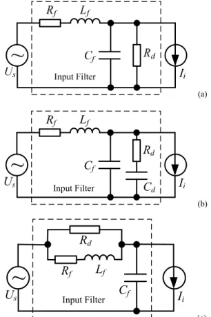
ESIGNThree general damped input filters for buck converters are shown in Fig. 7. They can also be used in matrix converter because of the matrix converter can be regarded as buck type converter in the input side. As the power supply of the matrix converter is usually AC voltages, the capacitors in the damped input filter should be bipolar capacitors. The topology shown in Fig. 7(a) uses a damping resistor paralleled with the capacitor to increase the damping factor, however, the power consumed by the damping resistor is too
PEDS2009
high. An improved RC damping circuit presented in Fig. 7(b) uses an extra bipolar capacitor connected with the damping resistor in series, the approach avoids the high power consumption problem of the damping resistor but the capacitance of the damping capacitor C
dis still large, which is undesirable for large volume and high cost. Fig. 7(c) shows a more suitable approach for damped input filter design, which uses a resistor paralleled with the inductor of input filter to increase the damping factor of the LC filter.
(a)
~
L
fC
fU
sI
iR
fR
dC
d Input Filter(b)
~ Lf C
U
s fI
iR
fR
dInput Filter
(c) Fig. 7. Topologies to increase the damping factor of buck converter.
The voltage and current relationships of the input filter shown in Fig. 7(c) can be described by transfer functions, and the input current transfer function can be obtained as (10).
( )
( ) ( ) ( )
( ) ( ) ( )
d f f
s i s
d f f
s i f i
R R sL
U s U s I s
R R sL I s I s sC U s
+
⎧ − =
⎪ + +
⎨ ⎪ − =
⎩
(9)
( ) ( ) ( ) ( ) ( )
s Ud s Id i
I s = H s U s + H s I s (10)
2
( )
( ) ( ) ( )
f d f f
Ud
d f f d f f f d f
sC R R sL H s
s R L C s R R C L R R
+ +
= + + + + (11)
( )
2( ) ( )
d f f
Id
d f f d f f f d f
R R sL
H s s R L C s R R C L R R
+ +
= + + + + (12)
It could be found that the denominator of H
Ud(s) and H
Id(s) is the same and the characteristic frequency ω
nand the damping factor ζ of the two transfer functions are
d f
n
d f f
R R R L C
ω = + (13)
2 ( )
d f f f
d f f d f
R R C L R L C R R
ζ = +
+ (14) It could be found that when R
dÆ∞, the characteristic frequency (13) is the same to (7). This is the special case of open circuit of R
d. As the resistance of the inductor is usually few milliohms, without lose of accuracy, (13) and (14) could be simplified as
n
1/ L C
f fω = (15) 1
2
f
d f
L R C
ζ = (16) The frequency response waveforms of H
Id(s) are shown in Fig. 8. The inductance and capacitance are 1mH and 10μF, the same as Table I. In Fig. 8, ζ=5×10
-4, ζ=0.05, ζ=0.1 and ζ=0.5 are correspond to R
d=∞Ω, R
d=100Ω, R
d=50Ω and
Rd=10Ω. From Fig. 8 we can see there is a contradiction between the damping factor and filtering performance. The higher the damping factor, the worse the high-frequency attenuation capabilities. ζ=0.1 is selected here for a compromise solution, in this condition R
d=50Ω. The performance of the damped input filter is obtained by simulation, and the input current and output voltage of the filter are presented in Fig. 9.
From Fig.9 we can notice that the harmonic contents in the current and voltage waveforms are well eliminated respect to that of Fig. 3 in steady state operation of matrix converter.
The output current waveform is also improved. The start-up performance of the input filter is shown in Fig. 10. The FFT analysis of input current in steady state and start-up process are showed in Fig. 11 and Fig. 12, respectively. The FFT results show that the harmonic contents near the resonant frequency have been well eliminated.
Amplitude(dB)Phase (deg)
Fig. 8. Bode diagrams of HId(s).
PEDS2009
0 200
-400 -200
10ms/div
400 0
-15 15
0 -15 15 [A]
[V]
[A]
Ui
Io
Is
Fig. 9. Input LC filter performance obtained by simulation in steady state (ζ=0.1).
0 200
-400 -200
10ms/div
400
0 -400 600
0 30 200 -200
20
-10 400
10
Us
Ui
Is [V]
[V]
[A]
Fig. 10. Input LC filter performance obtained by simulation in start-up process (ζ=0.1).
Amplitude (%Fundamental)
Fig. 11. FFT analysis of input current waveform of the improved input filter in steady state (ζ=0.1).
0 1 2 3
×10-13
0 1000 2000 3000 4000 5000
Fudamental (Hz)
Fig. 12. FFT analysis of input current waveform of the improved input filter in start-up process (ζ=0.1).
It can be also found from Fig. 10 that the current spike in the start-up process is up to 21 Ampere, this is harmful to the
capacitor C
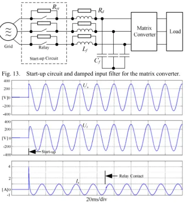
fof the filter and could cause EMI to the power system. A solution for this problem is to add a start-up circuit on the input side, which is shown in Fig. 13. A suitable time delay is inserted for capacitor C
fcharging, then the relays contact using the zero crossing signal of the input phase voltage. The start-up performance of the start-up circuit is investigated by simulation, the voltage and current waveforms obtained by simulation are shown in Fig. 14. It could be found that the input current spike has been reduced to a reasonable level.
Fig. 13. Start-up circuit and damped input filter for the matrix converter.
Fig. 14. Start-up process with improved start-up circuit.
V. E
XPERIMENTSA 5.5kW MC prototype with damped input LC filter has been built to testify the theory presented above. The parameter of the input filter is L
f=1mH, C
f=10μF and R
d=50Ω.
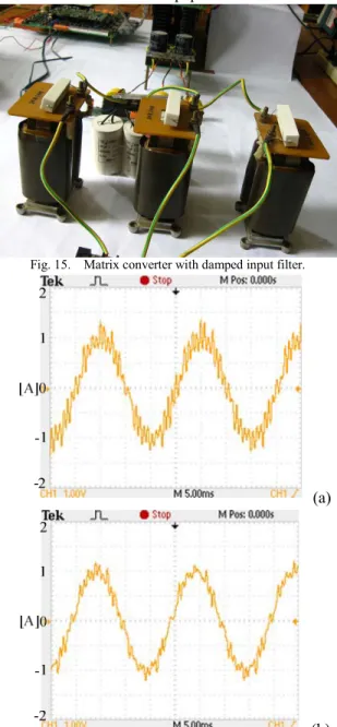
The matrix converter is constructed by eighteen discrete IGBTs. The digital control system of the prototype contains a MCU (TMS320LF2407A) and a FPGA (EP2C8). The cycle period of the digital control system is 200μs. The photo of the input filter with matrix converter is shown in Fig. 15.
The input filter has been tested in different damping resistor parameters. In experiment R
d=2kΩ and R
d=50Ω are tested, which are correspond to ζ=0.0025 and ζ=0.1. The input current waveforms of the input filter in steady state are presented in Fig. 16. It can be noticed that high damping resistor result in smooth input current waveform. The harmonic contents near the resonant frequency caused by the low damping factor have been well eliminated.
It could be found from Fig. 16(b) there are low frequency harmonic contents in the input voltage wavefom. It could be found the harmonic contents in the input current are caused
PEDS2009
by the low frequency harmonic contents in the input voltage, which will not discussed in this paper.
Fig. 15. Matrix converter with damped input filter.
(a)
(b)
Fig. 16. Input current waveforms. (a) Rd=2kΩ; (b) Rd=50Ω.VI. C
ONCLUSIONThe selection of inductor and capacitor of the input LC filter is presented in this paper by comprehensive review of the earlier literatures. For the output PWM current and start- up are both strong disturbances to the LC filter, the resonant phenomenon of LC circuit is mainly caused by low damping factor of the input filter. Method to improve the damping factor of input filter is then presented based on transfer function and frequency response methods. To avoid the current spike in the start-up process, a start-up circuit is proposed and good performance is exhibited. The validity of the damped input filter design has been verified by computer
simulation and experiment. The validity of start-up circuit will be investigated in future works.
R
EFERENCES[1] L. Huber and D. Borojevic, “Space vector modulated three-phase to three-phase matrix converter with input power factor correction. IEEE Transactions on Industry Applications,” vol. 31, no. 6, pp. 1234-1246, November/December 1995.
[2] IEEE Recommended Practices and Requirements for Harmonic Control in Electrical Power Systems. IEEE Standard 519-1992.
[3] M. M. Swamy and S. Rossiter, “Case studies on mitigating harmonics in ASD systems to meet IEEE 519-1992 standards,” Proceedings of IEEE IAS Annual Meeting, 1994: 685–692.
[4] P. Wheeler and D. Grant, “Optimised input filter design and low-loss switching techniques for a practical matrix converter,” IEE Proceedings of Electric Power Applications, 1997, 144(1): 53-60.
[5] T. Kume, K. Yamada, T. Higuchi, E. Yamamoto, H. Hara, T. Sawa, and M. Swamy, “Integrated Filters and Their Combined Effects in Matrix Converter,” IEEE Transactions on Industry Application, vol. 43, no. 2, pp. 571-581, March/April 2007.
[6] SU Mei, SUN Yao, QIN Heng-si. An Multi-objective Optimized Design of Input Filter of Matrix Converter. Proceedings of the CSEE, 2007, 27(1): 70-75(in Chinese).
[7] T. Podlesak, D. Katsis, P. Wheeler, J. Clare, L. Empringham, and M.
Bland, “A 150-kVA Vector-Controlled Matrix Converter Induction Motor Drive,” IEEE Transactions on Industry Applications. vol. 41, no.
3, pp. 841-847, May/June 2005.
[8] D. Casadei, J. Clare, L. Empringham, G. Serra, A. Tani, A. Trentin, P.
Wheeler, and L. Zarri, “Large-Signal Model for the Stability Analysis of Matrix Converters,” IEEE Transactions on Industrial Electronics, vol. 54, no. 2, pp. 939-950, April 2007.
[9] J. Andreul, I. Alegrial, I. Kortabarrial, S. Ceballos and I. Gabiola,
“Switching Frequency Behaviour for a Practical Matrix Converter,” in Proceedings of 32nd IEEE IECON Annual Meeting, 2006, Paris, France, pp. 1667–1672.
[10] C. Klumpner, P. Nielsen, I. Boldea, and F. Blaabjerg, “New Matrix Converter Motor (MCM) for Industry Applications,” IEEE Transactions on Industrial Electronics, vol. 49, no. 2, pp. 325-335, April 2002.
[11] D. Casadei, G. Serra, A. Tani, A. Trentin, and L. Zarri, “Theoretical and Experimental Investigation on the Stability of Matrix Converters,”
IEEE Transactions on Industrial Electronics, vol. 52, no. 5, pp. 1409- 1419, October 2005.
[12] AC7 Matrix Converter. Application Note, Yaskawa Electric America, 2008.
[13] M. Iftikhar, D. Sadarnac and C. Karimi, “Input Filter Damping Design for Control Loop Stability of DC-DC Converters,” Proceedings of ISIE 2007, IEEE International Symposium on Industrial Electronics, Vigo, Spanish, 2007, pp. 353-358.
[14] J. Andreu, J. Diego, I. Alegría, I. Kortabarria, J. Martín, and S.
Ceballos, “New Protection Circuit for High-Speed Switching and Start- Up of a Practical Matrix Converter,” IEEE Transactions on Industrial Electronics, vol. 55, no. 8, pp. 3100-3114, August 2008.