GaN Ultraviolet Photodetector with a Low-Temperature AlN
Cap Layer
S. J. Chang,a,zC. L. Yu,aP. C. Chang,band Y. C. Lina a
Institute of Microelectronics and Department of Electrical Engineering, Advanced Optoelectronic Technology Center, National Cheng Kung University, Tainan 701, Taiwan
b
Department of Electronic Engineering, Nan Jeon Institute of Technology, Yen-Hsui Township, Tainan County 737, Taiwan
We present the characteristics of GaN ultraviolet共UV兲 photodetectors 共PDs兲 with a low-temperature 共LT兲-AlN cap layer. With the LT-AlN cap layer, it was found that reverse leakage current became smaller by four orders of magnitude. With an incident wavelength of 360 nm, it was found that the responsivity under zero bias for the proposed PD was 0.063 A/W, which corresponds to a quantum efficiency of 21.7%. Furthermore, it was found that the UV to visible rejection ratio of the PD with a LT-AlN cap layer was larger than that of a conventional Schottky barrier PD.
© 2007 The Electrochemical Society. 关DOI: 10.1149/1.2722039兴 All rights reserved.
Manuscript submitted December 18, 2006; revised manuscript received February 14, 2007. Available electronically April 5, 2007.
GaN-based materials are useful in short-wavelength emitters such as light-emitting diodes and laser diodes. These materials are also useful for highly sensitive ultraviolet 共UV兲 photodetectors 共PDs兲.1,2
For example, GaN-based PDs can be used in space com-munications, ozone-layer monitoring, and flame detection. In the last few years, various types of GaN-based PDs have been demonstrated.3-5Compared with GaN-based p-n junction PDs, the epitaxial growth and device fabrication of Schottky barrier PDs are much simpler. The response speed of Schottky barrier PDs is also faster.6However, leakage current in Schottky barrier PDs is higher for a given applied bias.6,7Due to the large mismatches in lattice constant and thermal expansion coefficient between GaN and sap-phire, dislocation density in epitaxial layer is often high for GaN grown on sapphire. Thus, a leakage current problem in GaN-based Schottky barrier PDs will become severe. To reduce leakage current, we can insert an insulator between GaN and metal. Previously, it has been reported that SiO2, Ta2O5, Ga2O3, and Gd2O3can all serve as the insulator material of nitride-based metal-insulator-semiconductor devices.8-10However, these insulators were all ex situ deposited and contamination might occur at the insulator/semiconductor interface. Recently, it has been shown that one can in situ deposit a low-temperature共LT兲-GaN layer to reduce the leakage current of nitride-based Schottky barrier PDs and metal-semiconductor-metal PDs.11-13 However, it was also found that detector responsivity de-creased slowly as the wavelength of the incident light inde-creased from UV to the visible region due to the absorption of defect levels within the bandgap of the LT-GaN cap layer.11-13 Thus, UV-to-visible rejection ratio of the PDs with the LT-GaN cap layer became significantly smaller. Instead of LT-GaN, one may use LT-AlN to solve this problem. With a much larger bandgap, below bandgap absorption of LT-AlN should be less significant in the visible region. AlN with its high dielectric constant共i.e., 8.5兲 can serve as a good insulating material.14 Using capacitance-voltage 共C-V兲 measure-ments, Hashizume et al.14found that interface state density of LT-AlN/GaN is less than 1⫻ 1011cm−2eV−1. Later, Imanaga et al.15
found that leakage current of AlN/GaN heterostructure diodes
de-creases as the AlN growth temperature decreases from
990 to 650°C. These results suggest LT-AlN/GaN devices are promising. In this study, we report the fabrication of GaN-based PDs with LT-AlN cap layers. Properties of the fabricated devices are also discussed.
Samples used in this study were all grown by metallorganic chemical vapor deposition on 2 in. c-face sapphire 共0001兲 substrates.16-18 During the growth, trimethylgallium 共TMGa兲, trimethylaluminum共TMAl兲, and ammonia 共NH3兲 were used as
gal-lium, aluminum, and nitrogen sources, respectively. Disilane
共Si2H6兲 was used as the Si-doping source for the n-GaN layer. The
structure consists of a 30 nm thick LT-GaN nucleation layer, a 2m thick Si-doped GaN layer共n ⬇ 1018cm−3兲, a 0.3 m thick undoped
GaN layer共n ⬇ 1017cm−3兲, and a 30 nm thick LT-AlN cap layer
共i.e., PDគA兲. The growth temperature of LT-AlN was 600°C. For comparison, samples without the LT-AlN cap layer共i.e., PDគB兲 were also prepared. From X-ray diffraction共XRD兲 measurements, it was found that the full width at half-maximum 共fwhm兲 of the 共0002兲
GaN peaks observed from PDគA and PDគB were 170 and
168 arcsec, respectively. These values suggest that crystal qualities of the two samples were both good and similar. We also observed a broad and a weak LT-AlN related peak from PDគA.
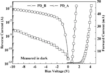
PDs were then fabricated. After mesa etching, we deposited Ti共13 nm兲/Al 共150 nm兲 followed by thermal alloying at 600°C for 8 min to serve as the ohmic contact. We then deposited semitrans-parent Ni共2 nm兲/Au 共4 nm兲 to serve as Schottky contact. The di-ameter of the fabricated circular PDs was 400m. A schematic diagram of PDគA is shown in Fig. 1. Figure 2 shows dark currents of the two PDs measured at room temperature. It can be seen that dark leakage current was significantly lower for PDគA. Such a reduction is attributed to the insertion of a LT-AlN cap layer, resulting in a thicker and higher potential barrier. With −5 V reverse bias, it was found that reverse leakage currents of PDគA and PDគB were 3.39 ⫻ 10−10 and 2.16⫻ 10−6A, respectively. Under forward bias, it
was found that turn-on voltages of PDគA and PDគB were 2.5 and 0.7 V, respectively. The 2.5 V turn-on voltage of PDគA is smaller than the 4.5 V turn-on voltage of previously reported PD with a LT-GaN cap layer.13It is known that resistance of the LT-GaN and LT-AlN depends on the thickness and trap density. Resistance of our 600°C-grown AlN cap layer is smaller than that of the previously reported GaN cap layer grown at 550°C.13Thus, we achieved a relatively smaller turn-on voltage from PDគA. Using the method
z
E-mail: [email protected] Figure 1. Schematic diagram of PDគA.
Electrochemical and Solid-State Letters, 10共6兲 H196-H198 共2007兲
1099-0062/2007/10共6兲/H196/3/$20.00 © The Electrochemical Society
H196
proposed by Lee et al.,19 we found that series resistances were 1.49⫻ 105 and 3.57⫻ 102⍀ for PDគA and PDគB, respectively.
The much larger turn-on voltage and series resistance observed from PDគA should be attributed to the highly resistive nature of the LT-AlN cap layer.
Figure 3 shows room-temperature spectral responses of the two fabricated PDs with zero bias. It can be seen clearly that the photo-responses were nearly constant in the above bandgap UV region 共i.e., smaller than 360 nm兲, while a sharp cutoff occurred at 360 nm for both samples. Because we performed the measurements at zero bias, we should be able to ensure that no gain was induced.20,21In other words, we could assume that the internal gain is 1 and the responsivity R for the fabricated PDs could be expressed by22-24
R = ⫻q hc
where, q, , h, and c are the external quantum efficiency, electron charge, incident wavelength, Planck constant, and speed of light, respectively. With an incident light wavelength of 360 nm, it was found that the responsivity for PDគA was 0.063 A/W. This value corresponds to an external quantum efficiency of 21.7%. It was also found that the responsivity at 360 nm for PDគB was 0.102 A/W, which corresponds to an external quantum efficiency of 35.1%. Such a dramatic difference could be attributed to the fact that some
photogenerated carriers are trapped in the LT-AlN layer.12,13 The inset of Fig. 3 shows measured responsivity at 360 nm as a function of applied bias for the two fabricated PDs. It was found that al-though measured responsivity increased with reverse applied bias for both PDs, it increased much more slowly for PDគA. Such a result suggests that the photoconductive gain in PDគA is smaller than that in PDគB.25It has been shown that internal gain is related to illumi-nation and trapping at the interface states.26,27We believe this inter-nal gain is related to the high dislocation density and poor metal/ semiconductor interface in PDគB. Similar to PDs with LT-GaN cap layer,13 our LT-AlN cap layer should be able to passivate surface defects on the undoped GaN layer and reduce interfacial defects. Thus, the photoconductive gain is less pronounced for PDគA. Here, we define the UV-to-visible rejection ratio as the responsivity mea-sured at 360 nm divided by the responsivity meamea-sured at 400 nm. With such a definition, we found that UV-to-visible rejection ratios were 6.09⫻ 103and 3.14⫻ 102for PDគA and PDគB, respectively.
Compared with PDគB, the larger UV-to-visible rejection ratio ob-served from PDគA should be attributed to its much smaller dark current. The slow decrease in the visible region observed from the PDs with the LT-GaN cap layer11-13was not observed in our PDគA. Thus, the UV-to-visible rejection ratio of PDគA is much larger than that observed from the PDs with the LT-GaN cap layer.11-13
Figure 4 shows C-V measurement of the two PDs. Under zero bias, it was found that the measured capacitances of PDគA and PDគB were 33 and 50 pF, respectively. The smaller total capacitance of PDគA could be attributed to the insertion of the LT-AlN cap layer and thus, an additional serial capacitance. Although the total capaci-tance of PDគA is smaller, its series resistance was much larger than that of PDគB due to the insertion of the highly resistive LT-AlN cap layer. As a result, the response speed of PDគA should be much slower than that of PDគB due to the larger RC delay time. In other words, there exists a tradeoff between dark leakage current, UV-to-visible rejection ratio, and response speed when we inserted a highly resistive LT-AlN layer on top of the conventional nitride-based PD. In summary, a GaN-based UV PD with a LT-AlN cap layer was proposed and fabricated. Compared with conventional Schottky bar-rier PDs, it was found that we can achieve smaller dark current and larger UV-to-visible rejection ratios by inserting the LT-AlN cap layer. However, the larger resistance-capacitance delay time may reduce the response speed of the PDs with the LT-AlN cap layer.
National Cheng Kung University assisted in meeting the publication costs of this article.
References
1. N. Biyikli, I. Kimukin, O. Aytur, and E. Ozbay, IEEE Photon. Technol. Lett., 16, 1718共2004兲.
2. S. J. Chang, C. L. Yu, R. W. Chuang, P. C. Chang, Y. C. Lin, Y. W. Jhan, and C. H. Chen, IEEE Sens. J., 6, 1043共2006兲.
3. S. J. Chang, T. K. Ko, Y. K. Su, Y. Z. Chiou, C. S. Chang, S. C. Shei, J. K. Sheu, Figure 2. Dark currents of the fabricated PDs measured at room
tempera-ture.
Figure 3. Room-temperature spectral responses of the fabricated PDs under zero bias. The inset shows measured responsivity as a function of applied bias for the fabricated PDs.
Figure 4. C-V characteristics of the fabricated PDs.
H197
Electrochemical and Solid-State Letters, 10共6兲 H196-H198 共2007兲 H197
W. C. Lai, Y. C. Lin, W. S. Chen, and C. F. Shen, IEEE Sens. J., 6, 406共2006兲. 4. J. K. Kim and J. L. Lee, J. Electrochem. Soc., 151, G190共2004兲.
5. J. L. Li, W. R. Donaldson, and T. Y. Hsiang, IEEE Photon. Technol. Lett., 15, 1141 共2003兲.
6. M. Razeghi and A. Rogalski, J. Appl. Phys., 79, 7433共1996兲.
7. A. P. Zhang, G. T. Dang, F. Ren, H. Cho, K. P. Lee, S. J. Pearton, J. I. Chyi, T. E. Nee, C. M. Lee, and C. C. Chuo, IEEE Trans. Electron Devices, 48, 407共2001兲. 8. H. C. Casey, Jr., G. G. Fountain, R. G. Alley, B. P. Keller, and S. P. DenBaars,
Appl. Phys. Lett., 68, 1850共1996兲.
9. L. W. Tu, W. C. Kuo, K. H. Lee, P. H. Tsao, C. M. Lai, A. K. Chu, and J. K. Sheu,
Appl. Phys. Lett., 77, 3788共2000兲.
10. C. T. Lee, H. W. Chen, and H. Y. Lee, Appl. Phys. Lett., 82, 4304共2003兲. 11. M. L. Lee, J. K. Sheu, Y. K. Su, S. J. Chang, W. C. Lai, and G. C. Chi, IEEE
Electron Device Lett., 25, 593共2004兲.
12. S. J. Chang, M. L. Lee, J. K. Sheu, W. C. Lai, Y. K. Su, C. S. Chang, C. J. Kao, G. C. Chi, and J. M. Tsai, IEEE Electron Device Lett., 24, 212共2003兲.
13. M. L. Lee, J. K. Sheu, W. C. Lai, Y. K. Su, S. J. Chang, C. J. Kao, C. J. Tun, M. G. Chen, W. H. Chang, G. C. Chi, and J. M. Tsai, J. Appl. Phys., 94, 1753共2003兲. 14. T. Hashizume, E. Alekseev, D. Pavlidis, K. S. Boutros, and J. Redwing, J. Appl.
Phys., 88, 1983共2000兲.
15. S. Imanaga, F. Nakamura, and H. Kawai, Jpn. J. Appl. Phys., Part 1, 40, 1194 共2001兲.
16. W. C. Lai, S. J. Chang, M. Yokoyama, J. K. Sheu, and J. F. Chen, IEEE Photon.
Technol. Lett., 13, 559共2001兲.
17. S. J. Chang, W. C. Lai, Y. K. Su, J. F. Chen, C. H. Liu, and U. H. Liaw, IEEE J.
Sel. Top. Quantum Electron., 8, 278共2002兲.
18. S. J. Chang, C. H. Kuo, Y. K. Su, L. W. Wu, J. K. Sheu, T. C. Wen, W. C. Lai, J. F. Chen, and J. M. Tsai, IEEE J. Sel. Top. Quantum Electron., 8, 744共2002兲. 19. J. I. Lee, J. Brini, and C. A. Dimitriadis, Electron. Lett., 34, 1268共1998兲. 20. O. Katz, V. Garber, B. Meyler, G. Bahir, and J. Salzman, Appl. Phys. Lett., 79,
1417共2001兲.
21. O. Katz, V. Garber, B. Meyler, G. Bahir, and J. Salzman, Appl. Phys. Lett., 80, 347 共2002兲.
22. M. Razeghi and A. Rogalski, J. Appl. Phys., 79, 7433共1996兲.
23. S. M. Sze, Physics of Semiconductor Devices, 2nd ed., p. 745, John Wiley, New York共1981兲.
24. E. Uiga, Optoelectronics, p. 208, Prentice Hall, Englewood Cliffs, NJ共1995兲. 25. H. Jiang, N. Nakata, G. Y. Zhao, H. Ishikawa, C. L. Shao, T. Egawa, T. Jimbo, and
M. Umeno, Jpn. J. Appl. Phys., Part 2, 40, L505共2001兲.
26. V. Adivarahan, G. Simin, J. W. Yang, A. Lunev, M. A. Khan, N. Pala, M. Shur, and R. Gaska, Appl. Phys. Lett., 77, 863共2000兲.
27. O. Katz, V. Garber, B. Meyler, G. Bahir, and J. Salzman, Appl. Phys. Lett., 79, 1417共2001兲.
H198 Electrochemical and Solid-State Letters, 10共6兲 H196-H198 共2007兲
H198