Anomalous increase in hot-carrier-induced threshold voltage shift
in n-type drain extended metal-oxide-semiconductor transistors
Jone F. Chen,1,a兲 Shiang-Yu Chen,1J. R. Lee,1Kuo-Ming Wu,2Tsung-Yi Huang,2and C. M. Liu2
1
Institute of Microelectronics, Department of Electrical Engineering, and Advanced Optoelectronic Technology Center, National Cheng Kung University, Tainan 70101, Taiwan
2
Taiwan Semiconductor Manufacturing Company, Hsinchu 30077, Taiwan
共Received 30 January 2008; accepted 4 March 2008; published online 19 March 2008兲
Anomalous increase in positive threshold voltage shift 共⌬VT兲 in n-type drain extended metal-oxide-semiconductor共DEMOS兲 transistors stressed under high drain voltage and gate voltage is observed. Charge pumping data and technology computer-aided-design simulations reveal that hot-electron injection and trapping in the gate oxide above channel region is responsible for⌬VT. Enhanced impact ionization rate resulted from the presence of large amount of negative oxide charge in channel region is identified to be the main mechanism for anomalous increase in ⌬VT. From the results presented in this letter, hot-carrier-induced anomalous increase in⌬VTcan become a serious reliability concern in DEMOS transistors. © 2008 American Institute of Physics. 关DOI:10.1063/1.2901878兴
To reduce chip size and cost in power applications, high-voltage devices integrated into mature complementary metal-oxide-semiconductor 共CMOS兲 process have attracted much attention recently.1–3Among many types of high-voltage de-vices, drain extended MOS共DEMOS兲 transistors are exten-sively used in display drivers. One major reliability concern in DEMOS transistors is hot-carrier reliability because de-vices are often operated under high drain voltage 共Vd兲 and high gate voltage 共Vg兲.4–7 It has been reported that hot-carrier-induced on-resistance 共Ron兲 degradation is much greater than threshold voltage shift 共⌬VT兲, indicating that hot-carrier-induced damage is mainly located in drift region.4,8In this letter, however, anomalous increase in posi-tive ⌬VT but small Ron degradation is observed in our DEMOS device stressed under high Vdand high Vg. Charge pumping data reveal that significant⌬VTis attributed to large amount of hot-electron injection and trapping in the gate oxide above channel region. Technology computer-aided-design 共TCAD兲 simulations suggest that enhanced impact ionization共I.I.兲 rate resulted from the generation of negative oxide charge in channel region is the main mechanism re-sponsible for anomalous increase in⌬VT. The effect of nega-tive oxide charge in channel region on vertical electric field 共Ey兲 of the device is also discussed.
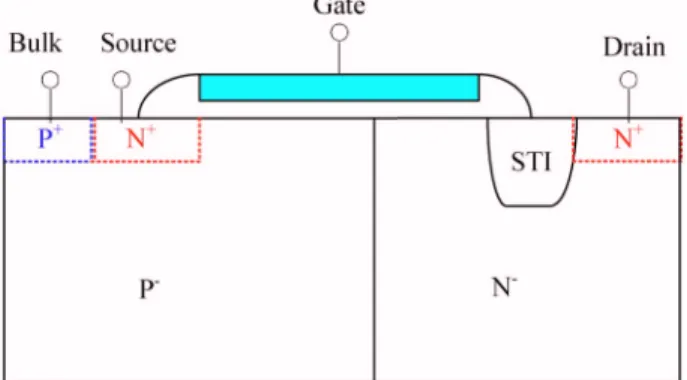
The device investigated in this letter is n-type DEMOS transistor processed by a 0.25m CMOS compatible high-voltage technology. Schematic cross section of the device is shown in Fig.1. The typical operation voltage of the device is 20 V for both Vd and Vg. dc hot-carrier stressing under
Vg= 20 V and various Vd is carried out at room temperature with the source and bulk terminals connected to the ground. To determine the bias condition in charge pumping measure-ment, flat-band voltage 共Vfb兲 and threshold voltage 共VT兲 in channel region are obtained from TCAD simulation. Vfband VTare defined as the Vg when the concentration at Si/SiO2 interface reaches 1014 cm−3 for hole and electron, respec-tively. From simulation results, Vfbis roughly −0.4 V, while
VTis about 1 V. The pulse with high level fixed at 4 V and low level共Vgl兲 varied from −0.4 to 2 V is applied to the gate under a frequency of 500 kHz. To extract hot-carrier-induced damage in the channel region, charge pumping current共Icp兲 is measured at source terminal while the drain is floating. From charge pumping data, a method similar to the one pro-posed by Cheng et al.8is used to extract hot-carrier-induced oxide charge density共⌬Not兲 and interface state density 共⌬Nit兲 in channel region. The stress tests are periodically inter-rupted to measure degradation of device parameters 共includ-ing VTand Ron兲 and Icp. VT is extracted at Vd= 0.1 V, while
Ron 共=Vd/Id, Id is drain current兲 is measured when Vd = 0.1 V and Vg= 20 V. In addition to stress tests, two-dimensional TCAD simulations are also performed and I.I. rate and Eyare analyzed to support the proposed degradation mechanism.
When the device is stressed under Vd= 26 V and the Vg to produce bulk current共Ib兲 maximum condition 共Vg⬇9 V兲 for 5000 s, both⌬VT 共1 mV兲 and Ron degradations 共⬍1%兲 are small. However, significant ⌬VT 共VT increases after stress兲 and some Ron degradations are exhibited when de-vices are stressed under Vg= 20 V with various Vd, as shown in Fig. 2. The time dependence of Ron degradation follows the expected power-law relationship. ⌬VT is small
a兲Electronic mail: [email protected]. FIG. 1.used in this letter.共Color online兲 Schematic cross section of the n-type DEMOS device APPLIED PHYSICS LETTERS 92, 113509共2008兲
0003-6951/2008/92共11兲/113509/3/$23.00 92, 113509-1 © 2008 American Institute of Physics
共⬍4 mV兲 during the early stage of stressing 共typically be-tween 101 and 102s兲. However, anomalous increase in ⌬VT is observed after about 102s. To investigate the physical degradation mechanism responsible for ⌬VT, Icp of the de-vice stressed under Vd= 26 V and Vg= 20 V is measured and shown in the rightward inset of Fig.3. Hot-carrier-induced ⌬Not in channel region is extracted from charge pumping data by
⌬Not=⌬VfbCox/q, 共1兲
where⌬Vfb is stress-induced shift in flat-band voltage and Coxis gate oxide capacitance.9The extracted⌬Notis shown in Fig.3 and the time dependence of ⌬Not is similar to the time dependence of⌬VT in Fig.2. On the other hand, hot-carrier-induced ⌬Nit can be extracted from a properly left-ward shift of Icpspectrum by the amount of⌬Vfb. The result-ing Icpdue to⌬Nitonly is shown in the leftward inset of Fig. 3. From the results in Fig.3, two distinct features are found. First, there is no apparent shift in Icp spectrum 共i.e., negli-gible⌬Not兲 during the early stage of stressing 共10 s兲. How-ever, a significant rightward shift in Icp spectrum 共i.e., sig-nificant negative⌬Not兲 is observed when the stressing is long enough共500, 1000, and 5000 s兲. Second, Icpincrease due to ⌬Nitis small, suggesting that⌬Nitis negligible. Such a result indicates that hot-electron injection and trapping in the gate oxide above the channel region is the main mechanism re-sponsible for positive⌬VT. The driving force of hot-electron injection is large Eyin the channel region and is discussed in the following paragraph.
To explain the anomalous increase in ⌬VT, normalized I.I. rate 共i.e., 兩Ib/Id兩, Ib/Id is bulk current兲 for the device
stressed under Vd= 26 V and Vg= 20 V is analyzed. As shown in Fig.4,兩Ib/Id兩 is close to unity during the early stage of stressing. However,兩Ib/Id兩 rapidly increases as the stress time is longer than 102s. In addition, Fig. 4 reveals that 兩Ib/Id兩 and ⌬VThave a similar anomalous increasing behav-ior, indicating that the anomalous increase in⌬VTis related to enhanced I.I. rate. To identify the mechanism responsible for enhanced I.I. rate, the effect of negative ⌬Not on the magnitude of I.I. rate and Eyis examined by TCAD simula-tions. Figures5共a兲and5共b兲show I.I. rate共where the impact ionization model proposed by Selberherr10 is used in simu-lation兲 and Ey 共along the dot line in the inset兲 under Vd = 26 V and Vg= 20 V for devices with or without the pres-ence of ⌬Not in the channel region. The origin of x axis in Fig.5共b兲 is the location of p−/n− junction and ⌬Not is uni-formly distributed between x = −0.8m and 0共where elec-tron injection probability is significant兲 in simulations. The amount of⌬Notis varied from small共5⫻1010cm−2兲 to large 共7⫻1011cm−2兲. The simulated ⌬V
Tis less than 4 mV when
FIG. 2.共Color online兲 Rondegradation shows the expected power-law rela-tionship.⌬VTis small during the early stage of stressing; however,
anoma-lous increase in⌬VTis observed after about 102s.
FIG. 3. 共Color online兲 Hot-carrier-induced ⌬Not in the channel region is extracted. Icpdata measured at various stress time are presented共rightward inset兲. The Icpspectrum due to⌬Nitonly is also extracted共leftward inset兲.
FIG. 4. 共Color online兲 During stressing, 兩Ib/Id兩 and ⌬VTshow a similar
anomalous increasing behavior, indicating that the anomalous increase in ⌬VTis related to enhanced兩Ib/Id兩.
FIG. 5.共Color online兲 Simulated 共a兲 I.I. rate and 共b兲 Eyunder Vd= 26 V and
Vg= 20 V for the devices with or without the presence of negative⌬Notin
channel region. I.I. rate and Eyare almost identical when small ⌬Not is
present. I.I. rate is greatly enhanced but Eyis reduced when large⌬Notis
present.
113509-2 Chen et al. Appl. Phys. Lett. 92, 113509共2008兲
⌬Not= 5⫻1010cm−2, while simulated ⌬VT is about 47 mV when ⌬Not= 7⫻1011cm−2. The relationship between ⌬VT and ⌬Not is similar in simulation and measurements when the above simulated ⌬VT results are compared to ⌬VT and ⌬Not data in Figs. 2 and 3. As shown in Fig. 5共b兲, large positive Ey 共favors for election injection into SiO2兲 in the channel region is exhibited, in agreement with the previous speculation that large Eyis the driving force of electron in-jection. Note that both I.I. rate and Ey are almost identical when small⌬Notis present, corresponding to small⌬VT dur-ing the early stage of stressdur-ing. However, when large amount of negative ⌬Not is present, significant positive mirror charges are induced in p− channel region, leading to the in-crease in effective doping in this region. Thus, as seen in Fig. 5共a兲, I.I. rate is greatly enhanced共especially near the p−/n− junction兲, leading to the anomalous increase in ⌬VT. From Fig.2,⌬VTseems to saturate when⌬VTis significant. This phenomenon can be explained by the reduction of Eywhen large ⌬Not is present as in Fig. 5共b兲. According to charge pumping data and simulation results, enhanced I.I. rate re-sulted from large amount of negative ⌬Not in the channel region is identified to be the main mechanism responsible for the anomalous increase in⌬VT.
In summary, hot-carrier-induced anomalous increase in ⌬VTin DEMOS transistors stressed under high Vd and high
Vg is examined. Hot-electron injection and trapping in the gate oxide above channel region causes positive ⌬VT. En-hanced I.I. rate during stressing resulted from the presence of large⌬Not is identified to be the main mechanism
respon-sible for the anomalous increase in⌬VT. The gradual satura-tion behavior in⌬VTwhen⌬VTis significant is attributed to the reduction of Ey. The results presented in this letter indi-cate that the anomalous increase in⌬VTmay become a seri-ous concern and should be taken into consideration in evalu-ating hot-carrier reliability of DEMOS devices.
1A. Moscatelli, A. Merlini, G. Croce, P. Galbiati, and C. Contiero, in
Pro-ceedings of IEEE International Symposium Power Semiconductor Devices and IC’s共IEEE, New York, 2000兲, p. 323.
2R. Zhu, V. Parthasarathy, V. Khemka, A. Bose, and T. Roggenbauer, in
Proceedings of IEEE International Symposium Power Semiconductor De-vices and IC’s共IEEE, New York, 2001兲, p. 403.
3T. Letavic, R. Cook, R. Brock, H. Effing, and R. Einerhand, in
Proceed-ings of IEEE International Symposium Power Semiconductor Devices and IC’s共IEEE, New York, 2005兲, p. 159.
4P. Moens, M. Tack, R. Degraeve, and G. Groeseneken, Tech. Dig. - Int. Electron Devices Meet. 2001, 877.
5J. F. Chen, K. M. Wu, K. W. Lin, Y. K. Su, and S. L. Hsu, in Proceedings
of IEEE International Reliability Physics Symposium共IEEE, New York,
2005兲, p. 560.
6P. Moens, G. V. den bosch, and G. Groeseneken, in Proceedings of IEEE
International Reliability Physics Symposium 共IEEE, New York, 2003兲,
p. 214.
7K. M. Wu, J. F. Chen, Y. K. Su, J. R. Lee, K. W. Lin, J. R. Shih, and S. L. Hsu,Appl. Phys. Lett. 89, 183522共2006兲.
8D. Brisbin, A. Strachan, and P. Chaparala, in Proceedings of IEEE
Inter-national Reliability Physics Symposium共IEEE, New York, 2002兲, p. 105.
9C. C. Cheng, K. C. Tu, T. Wang, T. H. Hsieh, J. T. Tzeng, Y. C. Jong, R. S. Liou, S. C. Pan, and S. L. Hsu, in Proceedings of IEEE International
Reliability Physics Symposium共IEEE, New York, 2006兲, p. 334.
10S. Selberherr, Analysis and Simulation of Semiconductor Devices 共Springer, Wien, 1984兲.
113509-3 Chen et al. Appl. Phys. Lett. 92, 113509共2008兲