行政院國家科學委員會專題研究計畫 成果報告
固態連續波雷射結晶於主動驅動有機電激發光顯示器低溫 複晶矽薄膜電晶體之研究
計畫類別: 個別型計畫
計畫編號: NSC94-2215-E-011-005-
執行期間: 94 年 08 月 01 日至 95 年 07 月 31 日 執行單位: 國立臺灣科技大學電子工程系
計畫主持人: 范慶麟
計畫參與人員: 楊宗憲、姜智淵、林政儀
報告類型: 精簡報告
處理方式: 本計畫可公開查詢
中 華 民 國 95 年 10 月 4 日
固態連續波雷射結晶於主動驅動有機電激發光顯示器 低溫複晶矽薄膜電晶體之研究
“Investigation of Low-Temperature Poly-silicon Thin-Film Transistors with Continuous-Wave Solid-State Laser Crystallization for Active-Matrix Organic light-Emitting Displays”
計畫編號:NSC 94-2215-E-011-005
執行期間:94 年 08 月 01 日至 95 年 07 月 31 日 主持人:范慶麟 台灣科技大學電子工程系助理教授
本計劃研究成果已刊登於 Japanese Journal of Applied Physics, Vol. 45, No. 36, 2006, pp. L973–L976
Abstract
We demonstrate the feasibility of continuous-wave laser crystallization (CLC) applied to product manufacturing with optimum laser parameters, paying particular attention to scan speed stability. With the optimized laser parameters, microscopic cracks at the interface between the buffer insulator and the crystallized polycrystalline silicon (poly-Si) film are significantly reduced. The optimization of laser parameters consists of increasing laser scan speed, decreasing scan speed deviation rate, and optimizing laser energy. We believe that CLC using the optimized laser parameters with a stable scan speed will provide a feasible and simple method for fabricating high-performance poly-Si thin-film transistors (TFTs).
中文摘要
主 動 驅 動 有 機 電 激 發 光 顯 示 器 (Active-Matrix Organic light-Emitting Displays;
AMOLEDs)具有高生命期、低秏電量與全彩面 板大型化等優點,將是未來中小尺寸面板的主 流。因此,用來驅動 AMOLEDs 的低溫複晶 矽薄膜電晶體 (Low-Temperture Poly-Silicon Thin-film Transistor; LTPS-TFT) 之技術開發 更顯得迫切。
AMOLEDs 對於驅動元件的要求除了高 驅動電流外,更要求元件具有高的均勻性及信 賴 性 。 本 計 劃 利 用 固 態 雷 射 源 (Solid-State Laser) 產 生 之 連 續 波 雷 射 (Continue-Wave
Laser) 取代現有的準分子雷射 (Excimer Laser) 來研製低溫複晶矽薄膜電晶體。從微調雷射參 數出發,並以材料分析驗証其薄膜結晶品質,
然 後 使 用 最 佳 化 的 雷 射 參 數 來 製 作 LTPS-TFT,並量測其元件特性,包含均勻性、
可靠度等。此外,並發展雙雷射源以製作出高 性能及高均勻性元件。最後,評估以此方法製 造出的 LTPS-TFT 應用在 AMOLEDs 的可行 性。
I. Introduction
There is an increasing interest in low-temperature (LT)-processed polycrystalline silicon thin-film transistors (poly-Si TFTs) for applications in display electronics, such as active-matrix liquid-crystal displays (AMLCDs) [1] and active-matrix organic light-emitting displays (AMOLEDs) [2]. Their primary advantage over conventional amorphous-silicon (α-Si) TFTs lies in their high driving current and the availability of both n- and p-channel TFTs.
These features facilitate the integration of high-performance complementary metal oxide semiconductor (CMOS) peripheral drivers with active switching elements on a single glass substrate, thus reducing the number of external connections for improved reliability and reduced cost [3]. Therefore, an integrated system- on-panel (SOP) high-performance poly-Si TFT with an enlarged grain size on a low-cost glass substrate is necessary. The channel films for
these devices are typically deposited in an amorphous phase, and are then crystallized to be in a large grain polysilicon phase with a low grain-boundary density. Excimer laser annealing (ELA) has been actively investigated as an alternative method for the crystallization of α-Si films [4-5]. The major advantages of this technique are the formation of polysilicon grains with excellent structural quality and the ability to process selected areas without thermal damage to the glass substrate. However, a grain size less than 100 nm as a result of the extremely high solidification velocity inherent to ELA has been a troublesome problem. In addition, non uniformity in laser-recrystallized poly-Si films may arise owing to laser beam overlap and poor pulse-to-pulse stability [6-7]. To cope with these problems, a number of schemes have been proposed to enlarge the grain size and improve the uniformity of poly-Si films [5-7]. Recently, low-cost easily maintained solid-state continuous-wave laser crystallization (CLC) [8-11] and a high-frequency pulse solid-state laser [12] (SSL) have been developed, which allows the growth of crystals as large as 3 × 20 μm2 extending along the laser scanning direction, resulting in high-performance poly-Si TFTs with excellent uniformity. However, the scan speed of high-frequency pulse SSL is very low (~mm/s) in order to connect the small grains formed at each pulse, resulting in low throughput in fabrication manufacturing. The CLC technique makes it easy to form large grains with high scan speed and wide energy range because of continuous energy supply, leading to a high-throughput process in product manufacturing. Unfortunately, the long melting time (~ 1 ms) due to the continuous energy supply induces random microscopic cracks at the interface between the buffer insulator and the crystallized poly-Si film as well as impurity diffusion from the substrate, resulting in product quality issues. Various measures [8-11] have
been reported to reduce the microscopic cracks between the buffer insulator and the crystallized poly-Si film. Thus, the feasibility and mechanism of CLC is unclear.
In this work, we will investigate and demonstrate the feasibility of the CLC technique applied to product manufacturing from the viewpoint of optimized laser parameters, particularly scan speed stability. To our knowledge, the correlation between scan speed stability and microscopic cracks has not been investigated. We believe that CLC using optimized laser parameters with a stable scan speed will provide a feasible and simple method for fabricating large grained poly-Si film for high-performance poly-Si TFTs on inexpensive glass substrates.
II. Experiment
Self-aligned top-gated n-channel solid-state CLC poly-Si TFTs were fabricated on a 100-nm-thick plasma-enhanced chemical vapor deposition (PECVD) silicon nitride and followed by a 400-nm-thick PECVD silicon-dioxide- covered 1737 Corning glass substrate according to the following procedures. A 100-nm-thick PECVD α-Si layer was first deposited using a SiH4 process at 350 ℃, followed by annealing at 450 ℃ to reduce the hydrogen content. All specimens were then crystallized using a scanning solid-state CW laser at room temperature in ambient air. A stable diode- pumped solid-state (DPSS) CW laser [532 nm (second harmonic (2
ω
) of Nd:YVO4)] was used.The power instability in the DPSS CW laser was less than 1% and the laser spot size was 200 × 10 μm2. No capping layer was formed on the Si film.
After laser annealing, the silicon film was patterned into individual active device islands, with a 120-nm-thick PECVD tetraethyl orthosilicate (TEOS) oxide deposited at 300 ℃ to serve as the gate insulator. A second poly-Si
film was subsequently deposited and patterned using reactive ion etching (RIE) dry etching to form the gate electrode. The source/drain and gate regions were then doped with phosphorus via self-aligned P+ ion implantation to a dose of 5 × 1015 cm-2, followed by thermal annealing at 600 ℃ for 6 h in N2 ambient. A 500-nm-thick PECVD-TEOS passivation oxide was then deposited at 300 ℃. After the contact holes were opened, the metallization of Al electrodes was completed, followed by sintering at 400 ℃ for 30 min in N2 ambient. Morphology images for the crystallized poly-Si films were obtained using optical microscopy (OM) and scanning electron microscopy (SEM). Thermal damage at the interface between the buffer insulator and the crystallized poly-Si film was confirmed by cross-sectional tunneling electron microscopy (TEM). The current-voltage characteristics of the fabricated devices were measured using an HP4145B semiconductor parameter analyzer.
III. Results and discussion
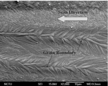
Figure 1 shows an SEM image of the crystallized poly-Si films fabricated by CLC with a laser energy of 4.1W at a rate of 10.5 cm/s in parallel traces. The image indicates that large-crystal growth starts from fine crystals located at the rim. Nucleation occurred at the edge region of the laser trace, and grain size increased toward the central region. This growth pattern may be explained by the temperature gradient during irradiation which leads to a colder rim region and a hotter center region [12].
During the solidification, grains grow laterally along the direction of laser scanning and push the liquid silicon toward the growth direction. At higher magnification, elongated crystallites can be observed extending obliquely from both rims of the laser trace to its center. The crystallites reach a length of more than 10 μm. In the final stage of solidification, when two growing grains meet to form the grain boundary at the central
region, a ridge develops. The grain boundaries are generally parallel to one another and to the laser beam scan direction. Moreover, it was found that there are some sub-grain boundaries.
The retarded nucleation at the rims upon optimizing the laser beam profile will be favored for undisturbed crystal growth in the center, and hence the occurrence of sub-grain boundaries will be decreased. The advanced studies of sub-grain boundaries are in progress. Note that the boundary energies of sub-grain boundaries are relatively low compared with those of random grain boundaries, and hence these defects in sub-grain boundaries are mostly electrically inactive and have a small effect on TFT performance. Only the boundaries in the center of the trace, where the grains originating from both rims meet, are electrically active random grain boundaries [13-14].
Fig. 1. SEM image of crystallized poly-Si films using CLC with laser energy of 4.1W at rate of 10.5 cm/s in parallel traces.
Figure 2 shows the dependence of grain size on irradiated laser energy. A change in the grain size increase rate is found to occur at a laser energy of 3.5 W. Below the turnaround point in laser energy (3.5 W), the silicon film is nearly solid during irradiation, causing a small change in grain size with laser energy. However,
Fig. 2. Dependence of grain size on irradiated laser energy of CLC for crystallized poly-Si films
above the turnaround point, the silicon film will be partially or completely molten, depending on irradiated laser energy, and crystallized by liquid-phase crystallization, resulting in a rapid increase in grain size with increasing laser energy. Thus, CLC makes it easy to form large grains within a wide energy range, as shown in Fig. 2, because of the slow molten Si cooling rate due to the continuous energy supply and directional solidification caused by laser scanning.
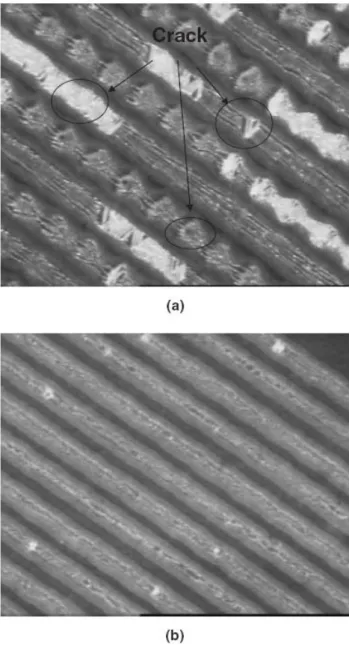
Figures 3(a) and 3(b) depict the correlation between the stability of laser scan speed and the morphology of the crystallized Si films. The scan speed is set at 10.5 cm/s for Figs. 3(a) and 3(b). The laser energy and the deviation rate in scan speed are 3.8W and 0.8 cm/s, respectively, for Fig. 3(a) and 4.1W and 0.3 cm/s, respectively, for Fig. 3(b). To discuss the correlation, the deviation rate in scan speed for Fig. 3(a) was intentionally designed to be larger than that for Fig. 3(b). In addition, to stress the effect of the deviation rate in scan speed on the film crack or temperature gradient, the laser energy for Fig.
3(b) was also intentionally designed to be higher than that for Fig. 3(a). In Fig. 3(a), cracks were
Fig. 3. Correlation between stability of laser scan speed and morphology of crystallized Si films. The scan speed is set at 10.5 cm/s for (a) and (b). The laser energy and the deviation rate in the scan speed are 3.8W and 0.8 cm/s, respectively, for (a) and 4.1W and 0.3 cm/s, respectively, for (b).
periodically produced in the irradiated Si films in each parallel trace. We presumed that the cracks were caused periodically owing to the inconsistent scan speed during the scanning process. Scanning was periodically slowed down, resulting in a longer melting time and an increase in temperature, leading to the cracks in the crystallized Si film as a result of the changing temperature gradient. Figure 3(b) shows the scan speed with a small deviation rate,
and the cracks in the Si film were significantly improved, even though the laser energy was higher than that for Fig. 3(a).
In CLC, the melting time is determined by speed and laser energy. From the perspective of a manufacturer, as fast a scan speed as possible is preferred to overcome the small laser beam size issue and to achieve high throughput.
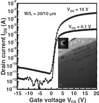
However, the faster the scan speed, the larger the scan speed deviation rate. A larger deviation rate will result in a longer melting time and cause an accumulation of heat, resulting in serious cracks in the crystallized Si films owing to the accumulated thermal stress between the melting silicon layer and the buffer insulator. On the other hand, the increasing laser energy will increase the melting time, resulting in increased grain size. However, at the same time, the probability of cracking is increased owing to the increasing thermal stress between the melting silicon layer and the buffer insulator. Thus, a higher laser energy will require a higher scan speed to decrease the melting time. Thus, the trade-off between high scan speeds, small deviation rates in scan speeds, and increased laser energy should be considered. The above discussion is confirmed by cross-sectional TEM analysis, showing that no thermal damage was induced in the glass substrate under the optimum conditions of 4.1W laser energy, 10.5 cm/s scan speed, and lower than 1% deviation rate, as shown in the inset in Fig. 4. The cross-sectional TEM analysis of poly-Si film shows a clear interface between the glass substrate and the buffer insulator. The interface between the buffer insulator and the crystallized poly-Si film is also clear. Figure 4 shows the typical transfer characteristics (IDS–VGS) of the LT poly-Si TFTs crystallized by the CLC technique using the same optimum conditions as for the inset in Fig.
4, measured at drain voltages VDS of 0.1 and 10 V. The field-effect mobility (
μ
FE) is calculated from the maximum value of the transconduc-tance at VDS = 0.1 V. Using the optimum laser conditions, the
μ
FE of the TFT is 234 cm2/(v·s), which is indicative of high-quality crystallized regions.Fig. 4. Typical transfer characteristics (IDS–VGS) for LT poly-Si TFTs crystallized by CLC with optimized laser parameters, including laser energy of 4.1 W, scan speed of 10.5 cm/s, and scan speed deviation rate below 1%. The inset shows a TEM cross-sectional image of between a crystallized poly-Si film and a glass substrate.
IV. Conclusion
The feasibility of CLC applied to product manufacturing with optimized laser parameters, particularly in the scan speed stability, has been demonstrated in this study. A higher laser energy will increase the grain size as a result of the increased melt time, but requires a high scan speed to avoid producing microscopic cracks.
However, the faster the scan speed, the larger the scan speed deviation rate. A larger deviation rate will result in a longer melt time, accumulating a larger amount of heat, therefore causing serious cracks in the crystallized Si films. Thus, the optimization of the laser parameters consists of increasing laser scan speed, decreasing scan
speed deviation rate, and optimizing laser energy.
These parameters should be considered and balanced simultaneously. With the optimized laser parameters, the microscopic cracks at the interface between the buffer insulator and the crystallized poly-Si film were significantly reduced. We believe that CLC, with the optimized laser parameters at a stable scan speed, will provide a simple method for fabricating high-performance poly-Si TFTs on inexpensive glass substrates.
Acknowledgements
The authors would like to acknowledge the financial support of the National Science Council (NSC) under Contract Nos. NSC 94-2215-E- 011-005 and the equipment support of the National Nano-Device Laboratory and Marketech International Corporation.
References
[1] B. C. Hseih, M. K. Hatalis and D. W. Greve: IEEE Trans. Electron Devices 35 (1988) 1842.
[2] M. Stewart, R. S. Howell, L. Pires and M. K. Hatalis:
IEEE Trans. Electron Devices 48 (2001) 845.
[3] H. Oshima and S. Morozumi: IEDM Tech. Dig., 1989, p. 157.
[4] T. Sameshima, S. Usui and M. Sekiya: IEEE Electron Device Lett. 7 (1986) 276.
[5] M. Miyasaka and J. Stoemenos: J. Appl. Phys. 86 (1999) 5566.
[6] A. Hara, K. Kitahara, K. Nakajima and M. Okabe:
Jpn. J. Appl. Phys. 38 (1999) 6624.
[7] H. Kuriyama, T. Kuwahara, S. Ishida, T. Nohda, K.
Sano, H. Iwata, S. Noguchi, S. Kiyama, S. Tsuda, S.
Nakano, M. Osumi and Y. Kuwano: Jpn. J. Appl.
Phys. 31 (1992) 4550.
[8] K. Kitahara, Y. Ohahi and Y. Katoh: J. Appl. Phys.
95 (2004) 7850.
[9] M. Tai, M. Hatano, S. Yamaguchi, T. Noda, S. K.
Park, T. Shiba and M. Ohkura: IEEE Trans. Electron Devices 51 (2004) 934.
[10] A. Saboundji, T. Mogammed-Brahim, G. Andra, J.
Bergmann and F. Falk: J. Non-Cryst. Solids 338–340 (2004) 758.
[11] Hara, K. Yoshino, F. Takeuchi and N. Sasaki: Jpn. J.
Appl. Phys. 42 (2003) 23.
[12] Y. Helen, R. Dassow, M. Nerding, K. Mourgues, F.
Raoult, J. R. Kohler, T. Mogammed-Brahim, R.
Rogel, O. Bonnaud, J. H. Werner and H. P. Strunk:
Thin Solid Films 383 (2001) 141.
[13] M. W. Geis, H. I. Smith, B. Y. Tsaur, J. C. C. Fan, D.
J. Silversmith and R. W. Mountain: J. Electrochem.
Soc. 129 (1982) 2812.
[14] N. Sotani, I. Hasegawa, D. Ide, T. Nohda and K.
Yamano: Jpn. J. Appl. Phys. 44 (2005) 21.