Visible electroluminescence from silicon nanocrystals embedded
in amorphous silicon nitride matrix
Liang-Yih Chen,a兲Wen-Hua Chen, and Franklin Chau-Nan Hongb兲
Department of Chemical Engineering and Center for Micro-Nano Technology, National Cheng Kung University, 1 University Road, Tainan, Taiwan, Republic of China
共Received 14 October 2004; accepted 24 March 2005; published online 5 May 2005兲
Visible electroluminescence from silicon nanocrystals 共Si-NCs兲 embedded in amorphous silicon nitride 共a-SiNx兲 films has been observed. The Si-NC/a-SiNxfilms were deposited by evaporating
silicon from electron gun into the inductively coupled plasma of nitrogen. The density of Si-NCs in the a-SiNx matrix was around 1012cm−2. Strong room temperature photoluminescence was
observed in 2.8 and 3.0 eV, different from literature values. The electroluminescence共EL兲 devices were fabricated with Si-NCs/ a-SiNxfilm as the active layer using the Al or Ca/ Ag cathode and the
indium tin oxide anode. Through tunneling, the electrons and holes were respectively injected from the cathode and anode into Si-NCs and confined within Si-NCs for light emission by the high band gap a-SiNxmatrix. For the device with Ca/ Ag cathode, the turn-on voltage was as low as 10 V and
the EL efficiency was about 1.6⫻10−1Cd/ A. The EL spectra consisted of two broad peaks centered around 2.5 and 2.8 eV. Our results demonstrate that Si-NCs/ a-SiNx nanocomposite films have
potentials to be fabricated into electroluminescence devices using the low work function cathode. © 2005 American Institute of Physics.关DOI: 10.1063/1.1925311兴
Since the observation of intensive visible light emission from porous silicon at room temperature,1silicon nanostruc-tures have received enormous interest and have been studied intensively for their potential applications in optoelectronics devices.2,3 The origin of visible light emission in porous Si remains under debate. Silicon nanostructure was originally believed to be responsible for the radiative recombination. Nevertheless, theoretical investigations further showed that the rupture of the translational symmetry in silicon nano-structure could cause the transition from indirect to direct band gaps, with a large increase in the probability of radia-tive recombination.4 Many problems remain to be solved in using porous Si for practical applications, such as the low efficiency in light emission under a bias, the instability of light emission due to spontaneous oxidation at ambient con-ditions, the sensitivity of luminescence to the preparation conditions, and the fragility in mechanical properties, etc.5
As an indirect band gap material, bulk Si is known to be inefficient in light emission. Besides, the low band gap of bulk Si at about 1.1 eV allows only for infrared emission, instead of visible light. Therefore, optoelectronic devices are currently built on compound semiconductors due to their high efficiency in light emission. Compound semiconduc-tors, however, are hard to integrate into cheap and versatile silicon circuits due to lattice mismatch problems. Once Si devices can be made exhibiting high electroluminescence 共EL兲 efficiency, the low cost and powerful optoelectronic integrated circuit Si devices will become feasible. Besides, due to mature processing technologies, the Si-based light-emitting diode共LED兲 may become a candidate for the next generation flat-panel display. Since the Si nanostructure has been believed to be responsible for the visible light emission in porous Si, various techniques have been attempted to im-prove the fabrication of Si nanostructures, including
chemi-cal vapor deposition,6 sputtering,7 Si ion implantation into SiO2 films,
8
cluster ion-beam deposition,9 laser ablation,10 etc.
Recently, silicon nanocrystals 共Si-NCs兲 embedded in a silica共SiOx兲 matrix have been demonstrated to emit visible
light by photoluminescence共PL兲 measurements. Sufficiently high efficiency of visible light emission with various colors could be observed from the Si-NCs/ a-SiOxcomposites, and
the PL intensity was high enough for LED applications.6,8,11 However, only a few papers have reported on the electrolu-minescence characteristics of Si-NCs/ a-SiOx,
12–14
mainly due to the difficulty of the tunneling of electrons and holes through the wide band gap oxide and their efficient optical recombination within the nanocrystals. Thus, silicon nitride, rather than oxide, is attempted as the matrix material due to its lower band gap for tunneling.
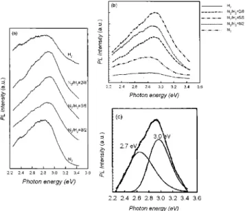
In this study, the optoelectronic nanocomposite films were deposited on Si共100兲 and indium tin oxide 共ITO兲 glass substrates at room temperature by e-beam evaporation of Si into the inductively coupled plasma 共ICP兲 in N2/ H2 gases. The deposited Si-NCs/ a-SiNx films were employed as the
active layer. Figure 1 shows the PL spectra of the films de-posited at various gaseous N2/ H2ratios. A Xe lamp operated at 150 W was employed as the excitation source for the PL spectra. The wavelength of excitation is 325 nm. The PL spectra show that the positions of emission peaks are insen-sitive to the N2/ H2ratios. However, the intensity reaches the maximum when the nitrogen is at 50% in the N2/ H2mixture. When starting to increase N2 in H2, the interface between silicon nitride and silicon starts to appear with the interface passivated by hydrogen, so that the PL intensity is enhanced. However, when increasing nitrogen above 50%, the ioniza-tion of nitrogen becomes low and the hydrogen passivaioniza-tion is also reduced, so that the PL intensity is decreased. In addi-tion, the emission peak can be deconvoluted into two broad peaks at 2.7 and 3.0 eV.
a兲Electronic mail: [email protected]
b兲
Electronic mail: [email protected]
APPLIED PHYSICS LETTERS 86, 193506共2005兲
0003-6951/2005/86共19兲/193506/3/$22.50 86, 193506-1 © 2005 American Institute of Physics
Since the band gap of bulk silicon is only 1.1 eV, the observed high-energy values of emission peaks at 2.7 and 3.0 eV are likely due to the quantum confinement effect 共QCE兲 from ultrafine nanoparticles. Figure 2 shows the im-age from high-resolution analytical electron microscopy 共HRAEM兲. Si-NCs were clearly observed to be embedded in amorphous silicon nitride matrix. The sizes of Si-NCs were in the range of 1 – 5 nm, and the density of Si-NCs was about 5⫻1012cm−2. The selective area diffraction ring confirmed the formation of Si crystallites. The nitrogen element map-ping of the film was further obtained using electron energy loss spectroscopy 共EELS兲 by measuring the N K edge at 400 eV. By comparing the EELS energy filter image with the corresponding transmission electron microscope共TEM兲 im-age, Si-NCs were clearly observed to be embedded in the silicon nitride matrix. Assuming spherical Si nanocrystals with finite barrier height and effective electron mass me* = 0.15m0, the band gap energy can be shifted to 2.7 or 3.0 eV when the Si crystal size reduces to 1 – 2 nm due to the QCE.
On the other hand, the emission peaks at 2.7 and 3.0 eV might also be ascribed to the electronic transitions of the interface states,wSi→ vN−and Siⴰ→Ev, as calculated by Robertson et al.15and experimentally verified by Mo et al.16 The active centers for light emission at 2.7 and 3.0 eV were not clear, either in the ultrafine nanoparticles around 1 – 2 nm or at the interface between Si nanocrystal and silicon nitride matrix.
The structure of the EL device was glass/ ITO/ Si-NCs/ Al. The thickness of the active layer measured by cross-sectional TEM was about 20 nm. In this study, we employed the ITO substrate as the anode and used a metal electrode as the cathode. The current density-voltage 共J-V兲 characteristics of the EL device under the forward bias are shown in Fig. 3共a兲. The ITO anode was positively biased and the metal cathode was negatively biased. The Si-NCs/ a -SiNxdevice exhibited significantly higher current densities 共800 mA/cm2兲 and electroluminescence intensities
共0.12 Cd/m2兲 than did the Si-NCs/a-SiO
xdevices. The EL
spectra were measured using a double-grating monochro-mator with a charge-coupled diode detector. The EL spec-trum, shown in Fig. 3共b兲, was deconvoluted into two broad peaks centered around 2.5 and 2.8 eV. The positions of two peaks are very close to those of the PL peaks.
The effects of the cathode material, Al or Ca/ Ag, on the current density and luminescence of the EL devices are also shown in Fig. 4. For the device with Al cathode, the turn-on voltage was around 14 V, above which the current density and luminance began to rise sharply. The maximal luminance was 0.12 Cd/ m2, and the maximal EL efficiency achieved FIG. 1.共a兲 PL spectra of the films deposited at various N2/ H2ratios,共b兲 the
intensity of photoluminescence as a function of nitrogen composition in the gas, and共c兲 the deconvolution of PL spectra at N2/ H2= 5 / 5 into two peaks: 2.7 and 3.0 eV.
FIG. 2. HRAEM image of the Si-NCs/ a-SiNxnanocomposite. The inset shows a selective area diffraction pattern of Si nanocrystals.
FIG. 3.共a兲 The characteristics of the current density 共J兲 and the luminance
共L兲 versus the forward bias voltage 共V兲 for the Si-NCs/a-SiNxfilm with the
Al cathode measured at room temperature, and共b兲 the corresponding EL spectrum. The inset in共b兲 is the photograph of EL device emission. The diameter of the pattern is about 2 mm.
193506-2 Chen, Chen, and Hong Appl. Phys. Lett. 86, 193506共2005兲
was about 6⫻10−4Cd/ A. By replacing Al with a Ca/ Ag cathode, the turn-on voltage could be reduced to 10 V, and the maximal luminance was increased to 0.25 Cd/ m2. The maximal EL efficiency achieved was 1.6⫻10−1Cd/ A, much higher than that for the Al cathode. Even at the maximal luminance, the Ca/ Ag cathode still outperformed the Al cathode 共e.g., luminance: 0.25 versus 0.12 Cd/m2, current density: 10.5 versus 7.8⫻103A / m2, voltage: 10 versus 14 V兲. Evidently, the Ca/Ag cathode improved the device performance by simultaneously increasing the current den-sity, the maximal luminance, and the EL efficiency.
Here, we deduced that the device performance should be dependent on the work function of the cathode material. The work functions of Ca/ Ag and Al are 2.8 and 4.3 eV, respec-tively. The electrons’ injection from the Ca/ Ag cathode to the lowest unoccupied molecular orbital states at nanocrys-tals is easier than that from the Al cathode due the lower energy barrier. Therefore, the current density and EL effi-ciency of the device with Ca/ Ag cathode are higher than those with the Al cathode. As suggested from the results just presented, the light emission mechanism in our devices is dominated by the injection of electrons and holes from the cathode and anode, respectively, and relies much less on the excitation of hot electron carriers by a high electric field. This conclusion is further supported by our observation that no light was emitted from the device under a reverse bias. In our devices, ITO also played an important role in injecting the holes into the highest occupied molecular orbital states at nanocrystals owing to its high work function of 4.7 eV. Our results suggest that the EL efficiency of the Si-NCs can be further improved by choosing appropriate cathode and anode materials.
In summary, Si-NCs were deposited by electron-gun evaporation of Si into the ICP of N2/ H2 in order to control the sizes of nanocrystals. In the PL spectra, the main emis-sion is a blue band 共3.0 eV兲 for the Si-NCs/a-SiNx
nano-composite film. The emission wavelength is much shorter than those共1.5–1.8 eV, red band兲 reported in the literature.17 For the EL devices containing Si-NCs/ a-SiNx, the J-V
curves exhibit diode characteristics. The EL efficiency of the Si-NCs/ a-SiNx device was also dependent on the cathode
and anode materials used. The Ca/ Ag cathode outperformed the Al cathode by simultaneously increasing the current den-sity, the maximal luminance, and the EL efficiency of the device. The ITO anode was essential for the hole injection owing to its high work function. For the EL device using ITO, Si-NCs/ a-SiNxand Ca/ Ag as the anode, active layer,
and cathode, respectively, the emission was observable with the naked eye through the ITO glass in the dark.
The authors are grateful for assistance from L. C. Wang for HRAEM analysis and Professor W. Chen for photolumi-nescence measurement. The support for this work from Na-tional Science Council, under contract no. NSC-93-2811-E-006-018, contract, and Center for Micro-Nano Technology, National Cheng Kung University is gratefully acknowledged.
1
L. T. Canham, Appl. Phys. Lett. 57, 1046共1990兲. 2
L. T. Canham, Nature共London兲 408, 411 共2000兲. 3
L. Pavesi, L. D. Negro, C. Mazzoleni, G. Franzo, and F. Priolo, Nature 共London兲 408, 440 共2000兲.
4
L. Brus, J. Phys. Chem. 98, 3575共1994兲; S. S. Iyer and Y. H. Xie, Science
260, 40共1993兲; T. Takagahara and K. Takeda, Phys. Rev. B 46, 15578
共1992兲.
5
M. A. Tischler, R. T. Collins, J. H. Stathis, and J. C. Tsang, Appl. Phys. Lett. 60, 639共1992兲.
6
N.-M. Park, T.-S. Kim, and S.-J. Park, Appl. Phys. Lett. 78, 2575共2001兲; B. H. Augustine, E. A. Irene, Y. J. He, K. J. Price, L. E. McNeil, K. N. Christensen, and D. M. Maher, J. Appl. Phys. 76, 4020共1995兲; D. J. Dimaria, J. R. Kertley, E. J. Pakulis, D. W. Dong, T. S. Kuan, F. L. Pesavento, T. N. Theis, J. A. Cutro, and S. D. Brorson, ibid. 56, 401 共1984兲; J. F. Tong, H. L. Hsiao, and H. L. Hwang, Appl. Phys. Lett. 74,
2316共1999兲.
7
S. Furukawa and T. Miyasato, Jpn. J. Appl. Phys. 27, L2207共1988兲. 8
T. S. Iwayama, S. Nakao, and K. Saitoh, Appl. Phys. Lett. 65, 1814 共1994兲; L.-S. Liao, X.-M. Bao, X.-Q. Zhang, N.-S. Li, and N.-B. Min, ibid. 68, 850共1996兲; K. Lutervá, T. Pelant, I. Mikulskas, R. Tomasiuas, D. Muller, J.-J. Grob, J.-L. Rehspringer, and B. J. Hönerlage, J. Appl. Phys.
91, 2896共2002兲. 9
M. Ehbrecht, B. Kohn, F. Huisken, M. A. Laguna, and V. Paillard, Phys. Rev. B 56, 6958共1997兲; G. Ledoux, J. Gong, and F. Huisken, Appl. Phys. Lett. 79, 4028共2001兲.
10
L. Patrone, D. Nelson, V. I. Safaov, M. Sentis, W. Marine, and S. Giorgio, J. Appl. Phys. 87, 3829共2000兲.
11
Y. Kanemitsu, T. Ogawa, K. Shiraishi, and K. Takeda, Phys. Rev. B 48,
4883共1993兲; L. Meda, E. Grilli, and M. Guzzi, Appl. Phys. Lett. 66, 851
共1995兲; J.-J. Wu, T.-C. Wong, and C.-C. Yu, Adv. Mater. 共Weinheim, Ger.兲
12, 1643共2002兲. 12
G. Franzò, A. Irrera, E. C. Moreira, M. Miritello, F. Iacona, D. Sanfilippo, G. Di Stefano, P. G. Fallica, and F. Priolo, Appl. Phys. A: Mater. Sci. Process. 74, 1共2002兲.
13
P. Photopoulos and A. G. Nassiopoulou, Appl. Phys. Lett. 77, 1816 共2000兲.
14
K. Luterová, I. Pelant, J. Valenta, J.-L. Rehspringe, D. Muller, J. J. Grob, J. Dian, and B. Hönerlage, Appl. Phys. Lett. 77, 2952共2000兲.
15
J. Robertson and M. J. Powell, Appl. Phys. Lett. 44, 415共1984兲. 16
C. M. Mo, L. Zhang, C. Xie, and T. Wang, J. Appl. Phys. 73, 5185共1993兲. 17
A. P. Li, I. Zhang, Y. X. Zhang, G. G. Qin, X. Wang, and X. W. Hu, Appl. Phys. Lett. 69, 4共1996兲; K. Chen, M. Wang, W. Shi, L. Jiang, W. Li, J. Xu, and X. Huang, J. Non-Cryst. Solids 198, 833共1996兲; G. F. Bai, Y. P. Qiao, Z. C. Ma, W. H. Zong, and G. G. Qin, Appl. Phys. Lett. 72, 3408 共1998兲.
FIG. 4. The characteristics of the current density共J兲 and the luminance 共L兲 versus the forward bias voltage共V兲 for the Si-NCs/a-SiNxfilm with the Ca/ Ag cathode measured at room temperature.
193506-3 Chen, Chen, and Hong Appl. Phys. Lett. 86, 193506共2005兲