行政院國家科學委員會專題研究計畫 成果報告
混模電磁干擾雜訊與濾波器設計之間的關聯性
計畫類別: 個別型計畫
計畫編號: NSC93-2218-E-002-143-
執行期間: 93 年 11 月 01 日至 94 年 10 月 31 日
執行單位: 國立臺灣大學電機工程學系暨研究所
計畫主持人: 陳德玉
計畫參與人員: 謝宏毅、李;忠樹、林;天麒、曾成德、莊湘微、
歐宗翰、林;育政
報告類型: 精簡報告
處理方式: 本計畫可公開查詢
中 華 民 國 95 年 1 月 11 日
基本資料
計畫主持人:陳德玉 教授
計畫參與人員(學生)
:謝宏毅、李忠樹、林天麒、曾成德、莊湘微、
歐宗翰、林育政
計畫名稱:混模電磁干擾雜訊與濾波器設計之間的關聯性
計畫編號:NSC93-2218-E-002-143
計畫執行起迄:2004.11.01 至 2005.10.31
執行機關:國立臺灣大學電機工程學系暨研究所
計畫核定日期:2004.11.11
報告應繳日期:2006.1.31
[1] 附件中之“Effects of X capacitors on EMI Filter Effectiveness”文章已呈現於
國際會議 IEEE Asia Pacific Symposium on EMC, 6-9 Dec. 2005.
[2] 附件中之“Use of a Cz Common-Mode Capacitor in 2-wire and 3-wire
Off-line Power Supplies” 文 章 已 呈 現 於 Taiwan Power Electronics
Conference, 2005。並在經由修改後已投出至國際會議 IEEE Internal Power
Electronics and Motion Control Conference, Portoroz, Slovenia, August 30
- September 1, 2006 等待審查。
國科會專題研究計畫成果報告
混模電磁干擾雜訊與濾波器設計之間的關聯性
計畫編號:NSC93-2218-E-002-143 計畫類別:個別型計畫
執行期限:93 年 11 月 1 日 至 94 年 10 月 31 日
計畫主持人:陳德玉 教授 E-mail:
[email protected]
計畫參與人員(學生)
:謝宏毅、李忠樹、林天麒、曾成德、莊湘微、歐宗翰、林育政
執行機關:國立臺灣大學電機工程學系暨研究所
第一部份 傳導性EMI 濾波器中之 X 電容的效應探討Effects of X capacitors on EMI Filter Effectiveness 摘要 對於切換式電源供應器之濾波器元件的設計探討 中,在X電容對於差模雜訊(DM noise;differential-mode noise)的抑制貢獻,可以劃分為兩個部份,一者為傳統之 阻抗不匹配(impedance mismatch)的概念,另一者為平 衡 由 寄 生 電 容Cp所 產 生 之Cp·(dv/dt) 混 模 雜 訊 電 流 (mixed-mode(MM)noise current balancing)的概念。 透過對於此兩現象機制的了解,我們能夠更加精確掌握濾 波器的設計,進而得到更緊密(compact)的濾波器設計 考量準則。最後再提出設計實例,來驗證理論與實務的一 致性。 第一章 簡介 電磁干擾(electromagnetic interference;EMI)濾波器, 雖然已被廣泛應用在切換式電源供應器中,用來解決傳導 性電磁干擾的問題。但至今仍存在有許多令人不解的部 份,常使工程師們必須花費許多時間在濾波器元件的選用 上。傳導性差模(DM)電磁干擾雜訊之干擾源可分為兩 部份,一者為濾波器元件間或與封裝環境間,所產生之鄰 近 電 磁 感 應 問 題 (proximity electromagnetic coupling effect),另一者為混模(MM)雜訊存在於差模(DM) 和共模(CM)之間的問題。一般而言,前者的問題發生 在頻譜頻率較高的部份,後者的問題發生在頻譜頻率較低 的部份,本研究著重於後者;即討論混模雜訊的現象。由 於混模雜訊的觀念與理論至今仍未被完全透析,以致於工 程師們對於傳導性濾波器的設計考量方面,仍存在著迷 思。本研究不僅著重於觀念釐清,此外還提出假設問題並 附上實驗結果,並驗證考慮混模雜訊效應來設計 EMI 濾 1-a 由寄生電容放電所產生之混模雜訊電流,此時功率晶 體為turned-on 狀態 1-b 由寄生電容充電所產生之混模雜訊電流,此時功率晶 體為turned-off 狀態 圖1 混模雜訊電流之耦合路徑 波器,確實能夠有效減少濾波器元件的體積,進而達成節 省成本之目的。 第二章 本質性差模雜訊(Intrinsic Differential-mode noise;IDM)與混模雜訊(Mixed-mode noise;MM) 傳導性電磁干擾雜訊可分為兩部份,差模雜訊(DM) 和共模雜訊(CM)。在最近的研究中,混模雜訊(MM) 逐漸被提及。混模雜訊是屬於差模雜訊中的一部分,他能 夠在橋式整流器(bridge diodes)中之四顆二極體關閉 (turned off)時被量測得到。然而有別於四顆二極體皆關 閉的傳統概念,其中一顆二極體會處在導通狀態,以致於 會產生高頻電流通過二極體,此高頻電流為寄生電容Cp所 產生之Cp·(dv/dt)混模雜訊電流。此電流會流經阻抗穩態網
2-a 零展開模式(zero span mode),without Cx
2-b 使用單一個平衡電容器(Cx)
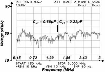
2-c 零展開模式(zero span mode),with Cx=0.68μF 圖2 在 200KHz時之DM noise時域波形(time-domain waveform)。系統之工作條件為:Vin(ac)=110V, Po=40W and
fs=50KHz
單一個電阻中,於是在量測差模訊時,利用頻譜分析儀中 的“零展開模式(zero span mode)”,可以觀察出混模雜 訊的存在。由於混模雜訊的產生機制類似共模雜訊,但卻 須由差模雜訊抑制元件來作壓制,於是稱其為作傳導性混 模電磁干擾雜訊。圖1 說明了混模雜訊經由寄生電容所產 生的耦合路徑。當功率晶體開啟(turned-on)時,寄生電 容會放電,由於此時橋式整流器僅單一顆二極體導通,所 以混模雜訊電流,便流經阻抗穩態網路中的單一個電阻, 圖3 典型 EMI 濾波器之示意圖 如圖1-a 所示。當功率晶體關閉(turned-off)時,寄生電 容會被充電,由於此時橋式整流器僅另單一顆二極體導 通,所以混模雜訊電流,便流經阻抗穩態網路中的另單一 個電阻,如圖1-b 所示。除了於圖 1 中所量測得到之差模 雜訊(MM noise)之外,其餘的部份;即在一對橋式整 流二極體導通的時段,所量測得到之差模雜訊,則統稱為 本質性差模雜訊(IDM noise),即傳統所謂的差模雜訊 (DM noise)。 為了可以實際的觀察到DM noise和IDM noise,我們利 用頻譜分析儀中的“零展開模式(zero span mode)”,能
夠觀察其個別雜訊的存在。圖2 為系統在 200KHz時之DM
noise時域波形(time-domain waveform),在圖2-a中,Period A為一對橋式整流二極體導通的時段,Period B為僅單一 顆二極體導通的時段。在Period A中被量測到的雜訊稱為 IDM noise,在Period B中被量測到的雜訊稱為MM noise。
當單一個平衡電容器(Cx)被使用後,若其電容器的阻抗 足夠小,則流經兩LISN電阻中的混模雜訊電流會被平 衡,如圖2-b中的虛線所示,因此在Period B中所量測到的 雜訊會大幅減小,如圖2-c中所示。注意,此時在Period A 中所量測到的雜訊衰減並無太大差別。於是由此觀之,對 於DM noise的衰減濾除,須由兩方面來著手,一者為須抑 制IDM noise,另一者為須抑制MM noise。圖 3 為典型EMI 濾波器之示意圖,傳統之X capacitors對於DM noise的抑 制,為阻抗不匹配(impedance mismatch)的概念;即X capacitor的阻抗若能遠小於所並聯元件之阻抗,則衰減的 效 益 將 會 十 分 的 明 顯 。 由 於 電 容 器Cx1並 聯 於LISN之 100Ω,而且電容器Cx2並聯於高阻抗之power supply端,所 以IDM noise由於阻抗不匹配的概念,能夠被有效的抑制。 然而對於MM noise的抑制準則,則與傳統之阻抗不匹 配的觀念大不相同。由於MM noise的現象,是由於LISN 中的兩個電阻,分別流經了由寄生電容所產生之Cp·(dv/dt) 的不平衡電流所導致,如圖1 所示。在使用了X capacitor 之 後 , 若 電 容 器 的 阻 抗 足 夠 小 , 則 流 經 於LISN
4-a complete diagram with EMI filter
4-b zero span mode (Top: Cx1=Cx2=0 and Bottom: Cx1=0, Cx2=0.22μF)
4-c zero span mode (Cx1=0, Cx2=0.22μF)
中兩個電阻的雜訊電流便能夠被平衡,於是所量測得到的 DM noise 會大幅減小,如圖 2 所示。所以 X capacitors 若 能符合公式(1)與公式(2),則能達到 MM noise 被壓制的結
果。因此X capacitor 對於 DM noise 的抑制,提供了兩方
4-d zero span mode (Cx1=0.68μF, Cx2=0.22μF) 圖4 Effectiveness of Cx1 and Cx2 under various conditions
5-a zero span mode (Cx1=0.68μF, Cx2=0.22μF)
5-b zero span mode (Cx1=0.68μF, Cx2=0)
面的作用,一為Impedance mismatch,另一方面作為平衡
電容。此兩方面對於雜訊的抑制準則概念大不相同。 第三章 一般常見之問題討論
問題一:完整的實驗架構如圖4-a所示。若Cx1和Cx2皆
5-c DM EMI noise (Cx1=0.68μF, Cx2=0.22μF)
5-d DM EMI noise (Cx1=0.68μF, Cx2=0)
圖5 Cx2 be removed and DM noise without much difference
圖6 Zero span mode (Cx1 can be effective in suppressing MM noise when Cx2 is not present)
的減少?或者甚至是消除掉其中之一顆X 電容?
回應一:當Cx1和Cx2同時應用在濾波器中時,依據
Impedance-mismatch和Mix-mode noise balancing的概念, 則仍有空間來作X電容的減少。依據圖 4-b所示,頻譜分 析 儀 採 用 零 展 開 模 式 (zero-span mode ) 來 觀 察
7-a zero span mode (Cx1=0, Cx2=0.22μF)
7-b zero span mode (Cx1=0, Cx2=0.68μF) 圖7 Increasing Cx2 does not help the overall DM noise
DM noise。比較皆未使用Cx1、Cx2 case和僅使用單一個Cx2 (= 0.22μF)case而言,則在Period B(MM)段的DM noise 有大幅度的降低,而在Period A(IDM)段的DM noise僅 只有小幅度的降低,其原因為MM noise已被平衡;符合 公式2 所示,而Impedance-mismatch的部分由於缺乏Cx1, 所以IDM noise仍大,如圖 4-b和圖 4-c所示。若此時加上 Cx1(= 0.68μF)於濾波器中時,Period A(IDM)段的DM noise則會被有效抑制,如圖 4-d所示。若Cx1(= 0.68μF) 已存在於濾波器中,並以符合公式 1 可平衡MM雜訊所 示,則電容Cx2可被宜除,而DM noise不會有太大影響, 如圖5 所示。 問題二:假如X 電容已經存在於濾波器中,將其放在 LISN-side 較好,還是放在 EUT-side 較好?
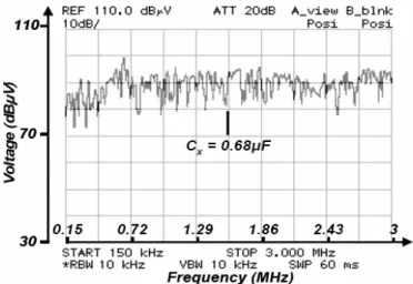
回應二:若MM noise 較 IDM noise 為大,則將 X-cap
放在EUT-side 較好,因為此時為了平衡 MM noise 所需的
公式 2,僅需要較小的 X-cap 電容值便可達成。若 IDM
8-a zero span mode in CM noise (Top: Cx=0.22μF and Bottom: Cx=0)
8-b zero span mode in CM noise (Top: Cx=0.68μF and Bottom: Cx=0)
8-c CM EMI noise (Cx=0)
因為此時是為了要達成Impedance-mismatch。不過由於使
了Cx1電容,所以MM noise也有達到被抑制的效果,如圖
6 所示,Cx1電容對於Period A(IDM)段的DM noise與Period B(MM)段的DM noise皆能達到有效的抑制。
問題三:為何有時增加X-cap 的值,但 DM noise 卻無
8-d CM EMI noise (Cx=0.68μF)
圖8 Increasing of CM noise due to usage of a Cx
法達到有效的抑制效果? 回應三:若X-cap 已經符合 MM noise 的平衡,並且 對於 Impedance-mismatch 的貢獻若不大,則增加 X-cap 的值便無法達到有效的抑制效果,如圖7 所示。 問題四:兩個串接的Y-cap 是否也能提供作為平衡電 容使用? 回應四:可以,只要其阻抗能夠符合公式 3,則兩個 串接的Y-cap 可以提供作為平衡電容使用。 問題五:X-cap 是否也會影響共模雜訊(common-mode noise)? 回應五:是的,X-cap 會增加共模雜訊的大小,並且隨著 電容的大小值增加而增加;即阻抗值減少而增加,如圖8 所示。 第四章 結論 DM noise 的 被 抑 制 , 一 部 份 依 靠 Impedance mismatch,另一部份依靠 MM noise balancing。數學分析
公式也被提出用來解釋MM noise balancing 的現象。所以
本研究有助於解決傳導性電磁干擾的問題,並且更能有助 於得到濾波器的最佳化分析。
References
[1] Shuo Wang, F.C. Lee, D.Y. Chen, W.G. Odendaal, “Effects of
parasitic parameters on EMI filter performance”, IEEE
Page(s):869 – 877.
[2] Dongbing Zhang, Dan Chen, D.Sable, “Non-intrinsic differential
mode noise caused by ground current in an off-line power supply”,
Power Electronics Specialists Conference, Volume 2, 17-22 May 1998 Page(s):1131 - 1133 vol.2.
[3] Qu, S. and Chen, D., “Mixed-mode EMI noise and its implications
to filter design in offline switching power supplies,” IEEE
Transactions on Power Electronics, Volume 17, Issue 4, July 2002 Page(s):502 - 507.
[4] Hung-I Hsieh, D. Chen, Song Qu, “A filter design procedure
incorporating mixed-mode EMI noise for off-line switching power supplies”, Power Electronics and Motion Control Conference,
Volume 3, 14-16 Aug. 2004 Page(s):1527 – 1532 Vol.3.
[5] M. J. Nave, Power Line Filter Design for Switched-Mode Power Supply. Chapter 5. New York: Van Nostrand Reinhild, 1991.
[6] Shuo Wang, F.C. Lee, W.G. Odendaal, “Improving the
performance of boost PFC EMI filters”, Applied Power
Electronics Conference and Exposition, Volume 1, 9-13 Feb. 2003 Page(s):368 - 374 vol.1.
第二部份
傳導性共模雜訊抑制電容(Cz)在兩線與三線式之切換式
電源供應器的使用探討
Use of a Cz Common-Mode Capacitor in 2-wire and 3-wire Off-line Power Supplies
摘要 在兩線式電源輸入之切換式電源供應器中,通常使用 一個電容來連接變壓器一次和二次側端點,其目的為了減 少傳導性電磁干擾雜訊中之共模雜訊。三線式電源供應器 有時也以此電容取代了傳統使用的 Y 電容,並達成抑制 共模雜訊的目的。雖然業界與學界應用此電容十分頻繁, 但是對於此電容之理論了解並不明確。在此篇文章中,針 對此電容對於雜訊的抑制過程,與此電容的動作機制作了 深入的解釋和探討,並且對於不同的轉換器架構,提供了 使用此電容的建議。在本文中也提及了變壓器的纏繞結 構,與轉換器的輸出電感位置的擺放,對於共模雜訊所產 生的效果,並且提供建議以達成抑制共模雜訊的目的。 第一章 簡介 由於兩線切換式電源轉換器應用在電池充電器和手 提式電子產品上十分普遍,但是此種系統多半是屬於兩線 式系統,即沒有第三隻地腳位(chassis ground)的存在, 所以在其傳導性共模(common-mode noise)電磁干擾雜 訊的抑制方面,便無法使用傳統之Y電容(Cy)元件來作 雜訊防治。一般而言在此種系統中,皆採用Z電容(Cz) 元件來作共模雜訊抑制。圖1 中為"Z電容"與"Y電容"之使 用示意圖。由於Z電容在學界與產業界已廣泛被使用,但 是對其為何能夠壓制共模雜訊的原理不甚清楚,在本研究 中已將其理論作完整的分析與解釋,並且提出模擬與實驗 的結果來驗證理論與實務的符合性。 第二章 Z 電容元件對於共模雜訊的抑制機制介紹 傳統之Y 電容應用在切換式電源轉換器中,對於抑制 所產生之傳導性共模(CM)電磁干擾雜訊如圖 2 所示。 若圖中之 Y 電容的阻抗足夠小,則共模雜訊電流會欲流 經Y 電容,所以流經 LISN 電阻中的剩餘共模雜訊電流便 較小,於是經由頻譜分析儀中所量測到之共模雜訊量便會 較小。若改採用Z 電容接在如圖 1 中之位置,則也能達到 共模雜訊抑制的效果,其原因為混模(MM)雜訊會使橋 式整流器中原本關閉的4 顆二極體,其中單一顆導通,如 圖1 "Z 電容"與"Y 電容"之使用示意圖
圖2 共模雜訊之耦合路徑示意圖(with two Cy capacitors)
3-a 由寄生電容充電所產生之混模雜訊電流(Q 為 turned-off 狀態) 3-b 由寄生電容放電所產生之混模雜訊電流(Q 為 turned-on 狀態) 圖3 儘單一顆二極體導通,此時Cz連接至輸入端;即L或 N 圖3 所示。當只有單一顆二極體導通時,Z電容會時續性 的接到電源端的L端(by D1)或接到電源端的N端(by D3),在輸入 60Hz電壓為正半週的時候;同樣的在輸入 60Hz電壓為負半週的時候,Z電容會時續性的接到電源端 的N端(by D2)或接到電源端的L端(by D4)。
圖4 Cz(以連接在點B和E之間為例)和寄生電容使得共 模雜訊更加嚴重 圖5 反馳式轉換器之兩線式系統 EMI 雜訊的量測 第三章 Z 電容元件的建議連接點選擇與漏電流的測試 適當的選擇 Z 電容的連接點能夠有效的抑制共模雜 訊,但Z 電容的連接點選擇若不適當,則會造成共模雜訊 更加嚴重。我們以返馳式電源轉換器的架構來做說明,如 圖4 所示。由於在 E 點存在著高頻的大電壓脈波,所以由 C·(dv/dt)會造成大電流經由寄生或 Z 電容流至地端,於是 便會使得共模雜訊更糟。 圖5 為返馳式(flyback)電源轉換器的電路架構圖, 若將電容接在點 A-B 和 C-B,則共模雜訊能夠得到有效 的抑制,若將電容接在點A-D、C-D、E-D 和 E-B,則會 導致共模雜訊更加嚴重。以模擬結果為例,如圖6 所示由 此可知,將Z 電容連接在兩固定電壓(大信號)準位上時, 共模雜訊才能夠得到有效的抑制。若連接至兩浮動電壓準 位,或其中之一連接至單一浮動電壓準位上時,則會導致 共模雜訊更加嚴重。以實驗結果為例,如圖7 所示由此可 知,將Z 電容連接在兩固定電壓(大信號)準位上時,共 模雜訊才能夠得到有效的抑制。若連接至兩浮動電壓準 位,或其中之一連接至單一浮動電壓準位上時,則會導致 共模雜訊更加嚴重。 Cz電容的漏電流的測試與Z電容值的選用相關,Z電容 值的選用可以視為兩Y電容的並聯,如圖 8 所示。 圖9 為順向式(forward)電源轉換器的電路架構圖, 若將電容接在點A-B、A-H、C-B 和 C-H,則共模雜訊能 導
6-a without a Z-cap
6-b Z-cap connected properly (between Pts. A and B)
6-c Z-cap connected improperly (between Pts. E and D)
圖6 反馳式轉換器之 CM 模擬雜訊電壓波形
夠得到有效的抑制,若將電容接在其餘的各點之間,則會
致共模雜訊更加嚴重。以模擬結果為例,如圖13 所示由
此可知,將Z 電容連接在兩固定電壓(大信號)準位上時,
7-a without a Z-cap
7-b Z-cap connected improperly (between Pts. E and D)
7-c Z-cap connected properly (between Pts. A and B)
圖7 反馳式轉換器之 CM 實驗雜訊電壓波形 位,或其中之一連接至單一浮動電壓準位上時,則會導致 共模雜訊更加嚴重。 圖10 為全橋式(full-bridge)電源轉換器的電路架構 圖,若將電容接在點A-B、A-G、C-B 和 C-G,則共模雜 訊能夠得到有效的抑制,若將電容接在其餘的各點之間, 則會導致共模雜訊更加嚴重。以實驗結果為例,如圖14 所示由此可知,將Z 電容連接在兩固定電壓(大信號)準
8-a testing of the leakage current in a three-wire system
8-b testing of the leakage current in a two-wire system 圖8 Setup of the leakage current test
圖9 順向式轉換器之兩線式系統 EMI 雜訊的量測
13-a without a Z-cap
位上時,共模雜訊才能夠得到有效的抑制。若連接至兩浮 動電壓準位,或其中之一連接至單一浮動電壓準位上時, 則會導致共模雜訊更加嚴重。 圖11 為半橋式(half-bridge)電源轉換器的電路架構 圖,若將電容接在點A-B、A-G、C-B、C-G、E-B 和 E-G, 則共模雜訊能夠得到有效的抑制,若將電容接在其餘的各
13-b Z-cap connected improperly (between Pts. E and D)
13-c Z-cap connected properly (between Pts. C and B)
圖13 順向式轉換器之 CM 模擬雜訊電壓波形 圖10 全橋式轉換器之兩線式系統 EMI 雜訊的量測 點之間,則會導致共模雜訊更加嚴重。同樣的,圖12 為 推挽式(push-pull)電源轉換器的電路架構圖,若將電容 接在點A-B、A-G、C-B 和 C-G,則共模雜訊能夠得到有 效的抑制,若將電容接在其餘的各點之間,則會導致共模 雜訊更加嚴重。 第四章 變壓器的結構與輸出電感的擺置對於共模雜訊的 抑制介紹
14-a without a Z-cap
14-b Z-cap connected improperly (between Pts. E and I)
14-c Z-cap connected properly (between Pts. A and G)
圖14 全橋式轉換器之 CM 模擬雜訊電壓波形 在變壓器中我們若採用不同繞線的方式,可得到大小不同 的寄生電容,經由透過將此寄生電容的適當安置,則共模 雜訊能夠被有效的抑制。如圖9 與圖 15 所示,依據圖 15-a 的變壓器繞線的方式所產生的效果,較圖 15-b 的效果為 佳,因為圖15-a 所產生之寄生電容恰位於穩定電壓點。
圖11 半橋式電源轉換器的電路架構圖。Z 電容接在點 A-B、A-G、C-B、C-G、E-B 和 E-G 時,則共模雜訊能夠 得到有效的抑制 圖12 推挽式電源轉換器的電路架構圖。Z 電容接在點 A-B、A-G、C-B 和 C-G 時,則共模雜訊能夠得到有效的 抑制
15-a larger CBC and smaller CED
15-b smaller CBC and larger CED
圖15 Forward converter transformer construction
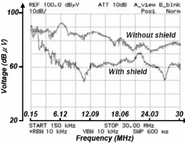
若採用在變壓器內部附上shielding 並將其接於穩定電
壓點處,如圖16 與圖 17 所示,則所產生之寄生電容,能
夠將共模雜訊作有效的抑制。
輸出電感的擺放位置對於共模雜訊也有影響,若將輸
出電感擺放在low-rail side(如圖 18-a),或分開成為兩個
電感(如圖18-b),則由於變壓器二次側皆為脈動電壓,
所以改便變壓器的結構並無法使共模雜訊被抑制,必須仍
要經由外接Z-cap 來抑制共模雜訊,如圖 19 所示。
圖16 Using shields placed between primary and secondary
圖17 CM noise measurement of Flyback converter. Transformer without and with shielding. Parasitic
capacitance between the shields is about 3300pF
18-a remove the output inductor and Z-cap improperly connected between Pts. C and B
18-b split the output inductor and Z-cap improperly connected between Pts. C and B
19-a Z-cap improperly connected between Pts. C and B
19-b Z-cap properly connected between Pts. C and G 圖19 CM voltage simulation of Forward converter with
output choke placement. 第五章 結論 本文章對於Z 電容元件於共模雜訊的抑制機制介紹, 作了詳細的解釋和探討,並且對於不同的轉換器架構,提 供了使用此電容的建議。此外也提及了變壓器的纏繞結 構,與轉換器的輸出電感位置的擺放,對於共模雜訊所產 生的效果,並且提供建議以達成抑制共模雜訊的目的。 References
[1] P. Chen, H. Zhong, Z. Qian, and Z. Lu, “The passive EMI
cancellation effects of Y capacitor and CM model of transformers used in switching mode power supplies (SMPS),” Power
Electronics Specialists Conference, June 2004, Aachen, Germany, pp. 1076–1079.
[2] S. Qu and D. Chen, “Mixed-mode EMI noise and its implications
to filter design in offline switching power supplies,” IEEE
Effects of X capacitors on EMI Filter Effectiveness
Hung-I Hsieh
Tien-Chi Lin
Dan Chen
Department of Electrical Engineering National Taiwan University
Taipei, Taiwan, R.O.C.
Abstract – The suppression mechanism of differential-mode noise of an X capacitor in off-line power supplies is attributed to two distinct concepts, impedance mismatch and C·(dv/dt) noise current balancing. Understanding of the two aforementioned mechanisms gives better insight into filter effectiveness which may lead to a more compact filter design. Several commonly raised questions about the effectiveness of X capacitors are answered with this theory and experimental supports.
Keywords – Mixed-mode (MM) EMI noise, impedance mismatching, noise current balancing
I. INTRODUCTION
EMI filters have been widely used for years to solve conducted EMI problems for off-line switching power supply applications. But even up to date, some sort of ‘cut-and-try” effort has been necessary in normal design process for the filter. Progress has been made in the recent past in this regard and better understanding of the problems has been achieved. However, in authors’ opinion there are two major problem areas that are still confounding to the designers. One is the proximity electromagnetic coupling problems in filter components and packaging environment [1]. The other area arises from the fact that there is a mixed-mode noise in addition to the differential-mode (DM) and common-mode (CM) noise conventionally associated with off-line power converters [2-5]. Generally speaking, the former problem area occurs in the upper end and the latter occurs in the lower end of the conducted EMI frequency spectrum.
This paper intends to address problems in the latter area. Discussions of mix-mode noise phenomenon have been reported in several recent papers [2-4]. However, the implications of the mix-mode noise theory have not been fully exploited yet for filter design purpose and to resolve some mysteries often cited by the designers. Investigation in this area revealed that some common questions confusing many designers in their efforts to minimize the filter size can be dealt with. Understanding of this intricate phenomenon can sometimes be very useful in solving their problems and may provide guidance for improving their designs.
II. INTRINSIC DIFFERENTIAL-MODE (IDM) NOISE AND MIXED-MODE (MM) NOISE
Conducted EMI noise is normally classified into two modes,
Q L1 Cp imm(t) D1 D4 D2 D3 Cb N L C1 C2 R2 R1 LISN L2 G D5 C3 R Cw Q L1 L1 Cp imm(t) D1 D4 D2 D3 D1 D4 D2 D3 Cb N L N L C1 C2 R2 R1 C1 C2 R2 R1 LISN L2 LISN LISN L2 G D5 C3 R D5 C3 C3 R Cw
1-a noise current flow during the “one diode conduction” period when Cp is being discharged
D1 D4 D2 D3 L1 LISN L2 C1 C2 R2 R1 N L imm(t) Q Cb G Cp D5 C3 R Cw D1 D4 D2 D3 D1 D4 D2 D3 L1 L1 LISN L2 LISN LISN L2 C1 C2 R2 R1 C1 C2 R2 R1 N L imm(t) Q Cb G Cp D5 C3 R D5 C3 C3 R Cw Cw
1-b noise current flow during the “one diode conduction” period when Cp is being charged
Figure.1 Illustration of mix-mode (MM) noise coupling
DM noise and CM noise. The recent addition, MM noise, accounts for some phenomenon unexplainable before. MM noise is actually part of the DM noise. It's the DM noise measured during the period when all the four bridge rectifying diodes of an off-line power supply are thought to be off. During this period, contrary to conventional thinking, one of the diodes actually conducts high- frequency C·(dv/dt) current through parasitic capacitances in the circuit, as pointed out first by [3]. This current, if flowing through the two LISN resistors with imbalance, accounts for the DM noise measured during that period. Because the generating mechanism of this noise is similar to that of CM noise but the suppression of the noise can be done with DM filter, it is called mix-mode noise. Fig.1 shows the paths of the C·(dv/dt) current in an off-line supply. The other part of the DM noise is measured during the period when one pair of the rectifying diodes conducts. This part of DM noise, called the Intrinsic Differential-mode (IDM) noise, is conventionally known as the DM noise. To see the MM noise and the IDM noise on a spectrum analyzer, one can use the "zero span" mode of the analyzer which displays the time-domain waveform of the noise spectrum at a selected frequency. Fig.2-a shows the time-domain waveform of the DM noise at the selected frequency at 200 KHz. In the figure, Period A is the diode conduction period, and Period B is the This work was supported by The National Science Council
of Taiwan under Award No.: NSC92-2218-E-002-051 and No.: NSC93-2218-E-002-143.
Vo lt ag e ( d B μV ) 100 60 20 Time (ms)
0 A: Diodes on (IDM) B: Diodes off (MM) 50
A B A B Vin(ac) Vo lt ag e ( d B μV ) 100 60 20 Vo lt ag e ( d B μV ) 100 60 20 Time (ms) 0
0 A: Diodes on (IDM)A: Diodes on (IDM) B: Diodes off (MM)B: Diodes off (MM) 5050
A B A B
A B A B
Vin(ac)
2-a zero span mode (without Cx)
D1 D4 D2 D3 C3 X cap L2 C1 C2 R2 R1 vac(t) N L G L1 LISN imm(t) Cx v1(t) v2(t) Q Cp R D5 C4 Flyback converter Cw D1 D4 D2 D3 C3 X cap L2 C1 C2 R2 R1 vac(t) N L G L1 LISN imm(t) Cx v1(t) v1(t) v2(t) v2(t) Q Cp R D5 C4 D5 C4 C4 Flyback converter Flyback converter Cw
2-b a balanced capacitor (X cap) is used
V o lt age ( d B μV ) 100 60 20 Time (ms) 0 A B A B 50 V o lt age ( d B μV ) 100 60 20 V o lt age ( d B μV ) 100 60 20 Time (ms) 0 5 0 AA BB AA BB 500
2-c zero span mode (with Cx=0.68 F)μ
Figure.2 Display of Time-domain waveforms of the DM noise. Circuit operating conditions: Vin(ac)=110V, Po=40W, Vo=12V and
switching frequency is 50KHz
period when only one diode conducts. The noise measured during Period A is called IDM, and called MM during Period B. When an X capacitor Cx is added to the circuit, as
illustrated in Fig.2-b, then the noise current through the two LISN resistors are balanced as indicated by the dotted lines. The MM noise is therefore much reduced for Period B as shown by Fig.2-c. Notice that very little noise attenuation occurs for IDM (Period A).
Filtering of the complete DM noise, therefore, must be considered into two parts: one for IDM and the other for MM noise. Using a typical EMI filter topology shown in Fig.3,
L C C R R G L LISN 50Ω 50Ω Cx1 LC EMI filter LD LD Cx2 Cy Cy G Power Supply AC Power Line L C C R R C C R R G L LISN LISN 50Ω 50Ω 50Ω 50Ω Cx1 LC EMI filter EMI filter LD LD LD LD Cx2 Cy Cy Cy Cy G G Power Supply AC Power Line
Figure.3 Typical EMI filter topology
explanation of DM filtering mechanism will be given below. The effectiveness of an X capacitor, according to conventional theory, depends on the degree of impedance mismatching [5]. That means that if the impedance of the X capacitor is much smaller than the impedance of the paralleled element, then the attenuation would be effective. The elements in parallel with the two X capacitors are the noise source impedance of the power supply (for Cx2) and the LISN 100-ohm resistor (for
Cx1). So, for an effective suppression of IDM noise, the X
capacitor used must be with low enough impedance compared to that of the respective paralleled element. For effective suppression of MM noise, however, the criterion is much different. The root cause of MM noise is the unbalance flow of high-frequency C·(dv/dt) current through the two LISN 50-ohm resistors as depicted in Fig.1. When an X capacitor Cx
is used, however, current flows through the two LISN resistors becomes balanced if the impedance of Cx is low compared to
the rest of the path. Fig.2 shows such a case. When the current path is balanced, the DM noise is much reduced, because DM noise is defined as the difference of the voltages across the two LISN resistors. Therefore, the effectiveness of Cx on MM
noise suppression depends on the degree of LISN current balancing. To be effective in his regard, the impedance of the X cap must be insignificant compared the impedance of the rest of the path. The condition is written down mathematically as follow: A. For Cx1: C j C Z x Cx ⋅ + << ⋅ = ω ω 1 50 1 1 1 Equation (1) B. For Cx2:
(
C D)
x C j L L C j C Z x =ω⋅ << + ω⋅ + ω⋅ + 1 50 1 2 2 Equation (2) where C2 is the 0.1uF capacitor inside LISN. 1/wc is usuallymuch less than 50 ohms.
An X capacitor is, therefore, serving both as an impedance-mismatching capacitor and a balancing capacitor. The effectiveness of each function depends on different criteria. For example, Cx1 is effective as an IDM filter only if
its impedance is small compared to LISN 100 ohms. But its effectiveness for suppressing MM noise lies on the inequality Eq.(1). Therefore, the same Cx1 exerts different influences on
L2 C1 C2 R2 R1 vac(t) N L LC LD LD Cy Cy D1 D4 D2 D3 C3 EMI filter G L1 LISN Q Cp Cx2 Cx1 R D5 C4 Flyback converter Cw L2 C1 C2 R2 R1 vac(t) N L LC LD LD Cy Cy D1 D4 D2 D3 C3 EMI filter G L1 LISN Q Cp Cx2 Cx1 R D5 C4 Flyback converter Cw R D5 C4 D5 C4 C4 Flyback converter Flyback converter Cw
4-a complete diagram with EMI filter (LD=100 H, μ LC=8.5mH,
Cy=3300pF). Circuit operating conditions: see Fig.2 caption.
V o lt age ( d B μV ) 110 70 30 Time (ms) Top: Cx1= Cx2= 0 Bottom: Cx1= 0 , Cx2= 0.22μF A B A B 0 50 V o lt age ( d B μV ) 110 70 30 V o lt age ( d B μV ) 110 70 30 Time (ms) Top: Cx1= Cx2= 0 Bottom: Cx1= 0 , Cx2= 0.22μF A B A B A B A B 0 50
4-b zero span mode (Top: Cx1=Cx2=0 and Bottom: Cx1=0,
Cx2=0.22 F)μ Cx1= 0 , Cx2= 0.22μF V o lt age ( d B μV ) 110 70 30 Time (ms) 0 50 A B A B Cx1= 0 , Cx2= 0.22μF V o lt age ( d B μV ) 110 70 30 Time (ms) 0 50 A B A B V o lt age ( d B μV ) 110 70 30 V o lt age ( d B μV ) 110 70 30 Time (ms) 0 0 5050 A B A B A B A B
4-c zero span mode (Cx1=0, Cx2=0.22 F)μ
III. ADDRESSING SOME COMMON QUESTIONS There are questions often raised by practicing engineers about the elusiveness of filter issues. Some of the questions are related to the IDM/MM issue. It should be pointed out that one cannot see the full picture by just looking at the total EMI noise. Better knowledge of the "behind-the-scene" CM, IDM, and MM noise would allow the designers to deal with the root causes and often end up with a more compact filter design. Answers to some commonly raised questions will be given below.
Question 1: If Cx1 and Cx2 already exist in a filter design
that meets the specification, how does one tell if there is still room for X capacitor reduction, either by reducing the
V o lt age ( d B μV ) 110 70 30 Time (ms) 0 50 A B A B Cx1= 0.68 μF , Cx2= 0.22μF V o lt age ( d B μV ) 110 70 30 V o lt age ( d B μV ) 110 70 30 Time (ms) 0 5 0 500 A B A B A B A B Cx1= 0.68 μF , Cx2= 0.22μF
4-d zero span mode (Cx1=0.68 F, Cμ x2=0.22 F)μ
Figure.4 Effectiveness of Cx1 and Cx2 under various conditions capacitance value or by eliminating one of the X capacitors?
Answer: Cx2 is in general not very effective for IDM noise
suppression because of low DM noise source impedance of an off-line power supply [5]. But is effective for MM noise suppression because it’s relatively easier to meet Eq.(2). On the other hand, Cx1 is relatively more effective for IDM
suppression because of paralleling with 100-ohm total LISN resistance but relatively poorer for MM noise suppression because Eq.(1) is more difficult to meet than Eq.(2) due to the presence of the inductors. The aforementioned assertion is supported by the experimental waveforms shown in Fig.4. Fig.4-a shows the complete circuit diagram including the complete EMI filter. Fig.4-b shows the time-domain display of DM noise at 170KHz for both cases, one without Cx1 and
Cx2, and the other with Cx1=0, but Cx2=0.22 F. μ One can see
that the suppression effect of Cx2 is very evident for Period B
(MM noise) but very little for Period A (IDM noise). However, when Cx1 is added, the suppression for Period A is very
evident hurt for Period B is slight because the circuit has already been balanced before Cx1 was added. Therefore, if
certain value of Cx1 is necessary for keeping IDM noise under
acceptable level, and that capacitance value is large enough to meet Eq.(1), then Cx1 plays the major role in suppressing both
IDM and MM noise. Cx2 would then plays minor role and can
be removed without much difference as shown in Fig.5. If the Cx1 value keeping IDM under acceptable level is not large
enough to also meet Eq.(1), then there are two options. One option is to keep Cx2 with value barely large enough to meet
Eq.(2). The other option is to eliminate Cx2 all together but
increase Cx1 value to the point that Cx1 meets Eq.(1).
Question 2: If only one X cap is allowed, is it better to put it on the LISN side or power-supply side?
Answer: That depends on the IDM noise level before any X capacitor is used. For the convenience of discussion in the paper, this level will be called the “pre-X cap” IDM level. If the pre-X cap IDM and MM level already exceeds the specification, then Cx1 should be used, i.e., an X cap should be
V o lt age ( d B μV ) 90 50 10 Time (ms) 0 50 Cx1= 0.68μF , Cx2= 0.22μF A B A B V o lt age ( d B μV ) 90 50 10 V o lt age ( d B μV ) 90 50 10 Time (ms) 0 5 0 5 Cx1= 0.68μF , Cx2= 0.22μF 0 0 A B A B A B A B
5-a zero span mode (Cx1=0.68 F, Cμ x2=0.22 Fμ )
V o lt age ( d B μV ) 90 50 10 Time (ms) 0 50 Cx1= 0.68μF , Cx2= 0 A B A B V o lt age ( d B μV ) 90 50 10 V o lt age ( d B μV ) 90 50 10 Time (ms) 0 5 0 5 Cx1= 0.68μF , Cx2= 0 0 0 A B A B A B A B
5-b zero span mode (Cx1=0.68 F, Cμ x2=0)
V o lt age ( d B μV ) 90 50 10 Frequency (MHz) 0.15 0.72 1.29 1.86 2.43 3 Cx1= 0.68μF , Cx2= 0.22μF V o lt age ( d B μV ) 90 50 10 Frequency (MHz) 0.15 0.72 1.29 1.86 2.43 3 Cx1= 0.68μF , Cx2= 0.22μF V o lt age ( d B μV ) 90 50 10 90 50 10 Frequency (MHz) 0.15 0.72 1.29 1.86 2.43 3 Cx1= 0.68μF , Cx2= 0.22μF 5-c DM EMI noise (Cx1=0.68 F, Cμ x2=0.22 Fμ )
placed on the LISN side. The Cx1 value would have to be
enough for both IDM suppression and meeting Eq.(1). Fig.6 shows the waveforms comparison when Cx1 value was
increased from 0.22 F to 0.68 F, which Cμ μ x2=0. It can be
seen that Cx1 is effective in suppression both IDM and MM
noise level when its value is increased. This does not contradict the answer to Question 1 in which it is asserted that Cx1 is in general more effective in suppressing IDM but not
V o lt age ( d B μV ) 90 50 10 Frequency (MHz) 0.15 0.72 1.29 1.86 2.43 3 Cx1= 0.68μF , Cx2= 0 V o lt age ( d B μV ) 90 50 10 Frequency (MHz) 0.15 0.72 1.29 1.86 2.43 3 Cx1= 0.68μF , Cx2= 0 V o lt age ( d B μV ) 90 50 10 90 50 10 Frequency (MHz) 0.15 0.72 1.29 1.86 2.43 3 Cx1= 0.68μF , Cx2= 0 5-d DM EMI noise (Cx1=0.68 F, Cμ x2=0)
Figure.5 Cx2 be removed and DM noise without much difference
90 50 10 Time (ms) V o lt age ( d B μV ) 0 50 Top: Cx1= 0.22μF, Cx2= 0 Bottom: Cx1= 0.68μF, Cx2= 0 A B A B 90 50 10 90 50 10 Time (ms) V o lt age ( d B μV ) V o lt age ( d B μV ) 0 50 Top: Cx1= 0.22μF, Cx2= 0 Bottom: Cx1= 0.68μF, Cx2= 0 A B A B A A B A B
Figure.6 Zero span mode (Cx1 can be effective in suppressing MM
noise when Cx2 is not present)
MM. Notice thatCx2=0 in the experiment leading to Fig.6.
When Cx2 is absent, there is no effective way to suppress MM
noise and the burden is shifted to Cx1. As long as Cx1 satisfies
Eq.(1), then it’s effective. But this may lead to a much larger Cx1 (than Cx2). On the other hand, if the pre-X cap IDM noise
level is below but the MM noise level is above the specification, then Cx2, the X cap on the power-supply side,
should be used. Cx2 as long as meets the condition of Eq.(2)
it’s fine. Fig.4-b shows the effectiveness of Cx2 on MM noise,
but not on IDM. But since IDM is not a concern in this case, it doesn’t matter. One can see from the answers to both Qusetions why the filter issue is so elusive. The solution depends a lot on particular condition and may not be generalized. Understanding of the issues allows sophisticated designers to have a better grip on this elusive subject. It should be pointed out that one-cap solution may not be optimal because two-cap solution may end up with less total capacitance.
Question 3: Why increasing the X capacitance value sometimes does not affect the total DM noise spectrum?
V o lt age ( d B μV ) 90 50 10 Time (ms) Cx1=0 , Cx2= 0.22μF A B A B 0 50 V o lt age ( d B μV ) 90 50 10 V o lt age ( d B μV ) 90 50 10 Time (ms) Cx1=0 , Cx2= 0.22μF A B A B A B A B A B A B 0 50
7-a zero span mode (Cx1=0, Cx2=0.22 F)μ
Vol ta g e ( d B μV ) 90 50 10 Time (ms) Cx1=0 , Cx2= 0.68μF A B A B 0 50 Vol ta g e ( d B μV ) 90 50 10 Time (ms) Cx1=0 , Cx2= 0.68μF A B A B 0 50 Vol ta g e ( d B μV ) 90 50 10 Vol ta g e ( d B μV ) 90 50 10 Time (ms) Cx1=0 , Cx2= 0.68μF A B A B A B A B A B A B 0 50
7-b zero span mode (Cx1=0, Cx2=0.68 F)μ
Figure.7 Increasing Cx2 does not help the overall DM noise
Answer: The zero-span waveforms used in the discussion tells the insight of the noise nature. The peak value of the waveform becomes the magnitude of the noise at that particular frequency in a normal frequency spectrum noise display. So, if MM noise dominates, and the X cap is primarily used for IDM suppression, then increasing X capacitance would not affect the MM noise, and therefore would not be noticeable from frequency spectrum display. On the other hand, if the total DM noise is dominated by the IDM noise, then increasing Cx2 may not be helpful to the total DM noise
because Cx2 is in general not very effective for IDM
suppression. Fig.7 illustrates this assertion. Increasing Cx2
does not help the overall DM noise.
Question 4: Can the two serially connected Y-capacitors alone be used as a balancing capacitor, i.e., for MM noise suppression? Should it be placed on the LISN side or the power-supply side?
Answer: Y capacitors alone can be a balancing cap as long as its impedance meets the balancing condition:
V o lt age ( d B μV ) 110 70 30 Time (ms) 0 50 Cx= 0.22μF Cx= 0 A B A B V o lt age ( d B μV ) 110 70 30 V o lt age ( d B μV ) 110 70 30 Time (ms) 0 50 0 50 Cx= 0.22μF Cx= 0 A B A B A B A B
8-a zero span mode in CM noise (Top: Cx=0.22 F and Bottom: μ
Cx=0) V o lt age ( d B μV ) 110 70 30 Time (ms) 0 50 Cx= 0.68μF Cx= 0 A B A B V o lt age ( d B μV ) 110 70 30 V o lt age ( d B μV ) 110 70 30 Time (ms) 0 50 0 50 Cx= 0.68μF Cx= 0 A B A B A B A B
8-b zero span mode in CM noise (Top: Cx=0.68 F and Bottom:μ
Cx=0)
(
C D)
y C j C j L L C Z y + ⋅ + ⋅ + << ⎟ ⎠ ⎞ ⎜ ⎝ ⎛ ⋅ ⋅ = ω ω ω 1 50 2 1 1 2 1 Equation (3) Because of the small Cy value normally used, the chance ofmeeting Eq.(3) is enhanced if there are chokes used in the filter. It’s easier to meet Eq.(3) if the Y capacitors are placed on the power-supply side. Because of relatively large CM noise source impedance associated with a power supply [5], it’s also better to put the y capacitor on the power-supply side for CM noise suppression.
Question 5: Does the use of Cx affect the CM noise?
Answer: That may. The fact that balancing provided by Cx
makes the two C·(dv/dt) current equal implies that CM noise, which is defined as the average of the two voltages across the LISN two 50-ohm resistors, will be increased. Fig.8 shows the increase of CM noise due to usage of a Cx.
V o lt age ( d B μV ) 110 70 30 Frequency (MHz) 0.15 0.72 1.29 1.86 2.43 3 Cx= 0 V o lt age ( d B μV ) 110 70 30 Frequency (MHz) 0.15 0.72 1.29 1.86 2.43 3 Cx= 0 V o lt age ( d B μV ) 110 70 30 110 70 30 Frequency (MHz) 0.15 0.72 1.29 1.86 2.43 3 Cx= 0 8-c CM EMI noise (Cx=0) Vo lt ag e ( d B μV ) 110 70 30 Frequency (MHz) 0.15 0.72 1.29 1.86 2.43 3 Cx= 0.68μF Vo lt ag e ( d B μV ) 110 70 30 110 70 30 Frequency (MHz) 0.15 0.72 1.29 1.86 2.43 3 Cx= 0.68μF 8-d CM EMI noise(Cx=0.68 Fμ )
Figure.8 Increasing of CM noise due to usage of a Cx
IV. CONCLUSIONS
Part of the DM noise is suppressed by impedance mismatching action and other part by balancing action of the X capacitors in EMI filters. The effectiveness of the two separate actions of an X capacitor varies with frequency, capacitance value, and filter topological arrangement. The phenomenon was explained, mathematical conditions for effective filter attenuation were pointed out in the paper. Discussions of how one may exploit this new understanding to make a more compact filter were given. The optimal solution often depends on particular conditions and cannot be generalized. Understandings of the issues allow sophisticated designers to have a better grip on this elusive subject.
REFERENCES
[1] Shuo Wang, F.C. Lee, D.Y. Chen, W.G. Odendaal, “Effects of parasitic parameters on EMI filter performance”, IEEE
Transactions on Power Electronics, Volume 19, Issue 3, May
2004 Page(s):869 – 877.
[2] Dongbing Zhang, Dan Chen, D.Sable, “Non-intrinsic differential mode noise caused by ground current in an off-line power supply”, Power Electronics Specialists Conference,
Volume 2, 17-22 May 1998 Page(s):1131 - 1133 vol.2. [3] Qu, S. and Chen, D., “Mixed-mode EMI noise and its
implications to filter design in offline switching power supplies,” IEEE Transactions on Power Electronics, Volume 17, Issue 4, July 2002 Page(s):502 - 507.
[4] Hung-I Hsieh, D. Chen, Song Qu, “A filter design procedure incorporating mixed-mode EMI noise for off-line switching power supplies”, Power Electronics and Motion Control
Conference, Volume 3, 14-16 Aug. 2004 Page(s):1527 - 1532
Vol.3.
[5] M. J. Nave, Power Line Filter Design for Switched-Mode
Power Supply. Chapter 5. New York: Van Nostrand Reinhild,
1991.
[6] Shuo Wang, F.C. Lee, W.G. Odendaal, “Improving the performance of boost PFC EMI filters”, Applied Power
Electronics Conference and Exposition, Volume 1, 9-13 Feb.
Use of a C
zCommon-Mode Capacitor in 2-wire and 3-wire Off-line Power Supplies
Hung-I Hsieh
Tien-Chi Lin
Dan Chen
Department of Electrical Engineering National Taiwan University
Taipei, Taiwan, R.O.C.
Abstract – In a two-wire input off-line power supply, a capacitor is often connected between the primary and the secondary side of the transformer for common-mode EMI reduction. For a three-wire off-line power supplies, such a capacitor, is also used sometime for the same purpose. It’s unclear how this capacitor works. In this paper, explanation of the noise suppression mechanism of such a capacitor is given. From the understanding of the mechanism, suggestions were made for the use of such a capacitor for transformer winding schemes and output inductor placement to avoid the pitfalls and achieve desirable effects. Keywords – Common-mode (CM) EMI noise, 2-wire system, 3-wire system
I. INTRODUCTION
Two-wire input off-line power supplies are popular in many battery charger applications for hand-held electronic devices. In such a system, there is no “chassis ground” connection point, which is available in a three-wire system. Figure.1 shows a circuit diagram of a three-wire off-line Flyback power supply in which the two so-called “Y capacitors” Cy are connected across
LINE (L) and NEUTRAL (N) to chassis ground (G). Y capacitors are normally effective and necessary for common-mode (CM) EMI reduction. In a two-wire system, however, there is no chassis ground available, and therefore Y capacitors cannot be connected as such. In such a system, a substituting capacitor Cz is often connected between the
primary and the secondary of transformer to reduce CM noise. In fact, similar connection using Cz as shown by the dotted line
connection in Fig.1, has been found even for some three-wire systems.
It’s not clear why this capacitor can be used to suppress CM noise. In this paper, explanation of the noise suppression mechanism of Cz will be given for both the two-wire and the
three wire systems. Understanding of such mechanism led to suggestions for alternative connection schemes, avoidance of pitfalls, and proper transformer construction. Discussion of the same issue for other power converter configurations will also be given. Throughout the paper, the term “Z capacitor” or Cz
will be used to mean the capacitor connecting the primary and the secondary, and Y capacitor or Cy will be used to mean the
capacitor connecting between either Line or Neutral and chassis ground.
II. NOISE SUPPRESSION MECHANISM OF A “Z” CAPACITOR
As shown in Fig.1, Y capacitors Cy are connected between G
D1 D4 D2 D3 L1 L2 Cy Cy C1 C2 R2 R1 vac(t) C3 N L Q D5 C4 R CM filter
LISN Flyback converter
Cz Chassis ground G D1 D4 D2 D3 D1 D4 D2 D3 L1 L1 L2 Cy Cy C1 C2 R2 R1 C1 C2 R2 R1 vac(t) C3 N L Q D5 C4 R CM filter
LISN CM filter Flyback converter
LISN Flyback converter
Cz
Cz
Chassis ground G
Figure.1 Using Y capacitors for common-mode EMI reduction in a three-wire
system. Capacitor Cz is sometimes used for the same purpose.
2C
yC·(dv/dt)
LISN
CM filter
25
Ω
v
CMG
Noise current2C
y2C
yC·(dv/dt)
LISN
LISN
CM filter
25
Ω
v
CM25
Ω
v
CMv
CMG
Noise currentFigure.2 Equivalent circuit of CM noise coupling
LISN L1 L2 C3 G N L Q D5 C4 R Flyback converter C B D E A F Cz C1 C2 R2 R1 D1 D4 D2 D3 vac(t) X Cp LISN L1 L1 L2 L2 C3 G N L Q D5 C4 R Flyback converter C B D E A A F F Cz C1 C2 R2 R1 C1 C2 R2 R1 D1 D4 D2 D3 D1 D4 D2 D3 vac(t) X Cp Cp
Figure.3 Measurement of EMI noise in a two-wire system
and, respectively, LINE and NEUTRAL. So, both LINE and NEUTRAL are always connected through a Cy to G. Figure.2
shows a simplified equivalent circuit of CM noise coupling to the LISN resistors. The Cdv/dt current source represents the displacement current going through a variety of parasitic capacitances in the system, including semiconductor switching device package-to-ground capacitances, transformer inter-winding capacitances, and parasitic capacitances between other components and ground point G. Y capacitors are used to provide a path to divert part of the Cdv/dt noise current from flowing into LISN and achieve CM noise reduction.
For a two-wire system, EMI noise measurement is normally conducted under the condition shown in Fig.3, in which the secondary side Point X is connected to LISN Ground which, in turn, is connected to G ground in the measurement setup. So, Pt. A is connected to L when one pair of diodes (D2, D4) conducts
and is connected to N when the other diode pair (D3, D1)
This work was supported by The National Science Council of Taiwan under Award No.: NSC92-2218-E-002-051 and No.: NSC93-2218-E-002-143.