國 立 交 通 大 學
影像與生醫光電研究所
碩
士
論
文
雙接面砷化鎵量子點太陽能電池之數值分析
Numerical Study of GaAs-Based Dual Junction Quantum Dot
Solar Cells
研 究 生:石謦毓
指導教授:林建中 助理教授
雙接面砷化鎵量子點太陽能電池之數值分析
Numerical Study of GaAs-Based Dual Junction Quantum Dot
Solar Cells
研 究 生:石謦毓 Student:Ching-Yu Shih
指導教授:林建中 Advisor:Chien-Chung Lin
國 立 交 通 大 學
影像與生醫光電研究所
碩 士 論 文
A ThesisSubmitted to Institute of Imaging and Biomedical Photonics National Chiao Tung University
in partial Fulfillment of the Requirements for the Degree of
Master In
Institute of Imaging and Biomedical Photonics, September 2012
Tainan, Taiwan, Republic of China
I
雙接面砷化鎵量子點太陽能電池之數值分析
學生:石謦毓 指導教授:林建中
國立交通大學影像與生醫光電研究所碩士班
摘要
我們提出了一種新的組合,即雙接面砷化鎵量子點太陽能電池和數值研究。我們建立了 我們的結構,並且使用 MATLAB® 以及商用軟體 Silvaco®和 APSYS®。通過修改後的吸收係數 k,和有效的量子點相關太陽能電池的帶隙的載子吸收適於一個適當的參雜物。 最後的計算示出的最佳效率增強功能是約 1.11 倍的非量子點的嵌入式太陽能電池。這 樣的設計有很大的潛力,實現三接面的串聯型太陽能電池。
II
Numerical Study of GaAs-Based Dual Junction Quantum Dot Solar
Cells
Student:Ching-Yu Shih Advisor:Dr. Chien-Chung Lin
Institute of Imaging and Biomedical Photonics
National Chiao Tung University
Abstract
A novel combination of quantum dot intermediate band solar cell and dual-junction tandem cell is proposed and studied numerically. We built our device model by using Matlab® coding and commercial software Silvaco® and APSYS®. A proper inclusion of quantum-dot-related carrier absorption is adapted through modified extinction coefficient k, and effective band gap of the device. The final calculation shows the optimal efficiency enhancement is about 1.11 times of the non-quantum-dot embedded device. This design has great potential to realize a triple junction result with a dual-junction photovoltaic device.
III
致謝
碩班兩年期間,轉眼就過去了,相當的不捨,首先感謝學問淵博及脾氣很好的林建 中老師,佛心來的收下了一個什麼都不會的我,且細心與耐心的教導,真的是辛苦老師 您了,學生我受益匪淺,於此獻上最深的敬意與感謝,論文口試承蒙中興大學電機系賴 聰賢老師以及交通大學照明與能源所蘇海清老師給予的指導及寶貴意見,使我的論文更 加完善而嚴謹,至此致上由衷的感謝。 在台南念書時是我人生中最美好的時光之一,威麟,印聰,禹軒,一正,孟勳,懷 翔在空曠的校園中有你們而充實。,感謝威麟,不厭其煩的教導與照顧,也是我心中的 榜樣。感謝中山大學光電所貴雅學姊,各方面的協助,總是幫忙我許多麻煩的事情,還 有感謝隆興學長的照顧。感謝哲斌,明瑄,禎佑,蕭亞,愷威,善允等的各位學弟在我 碩二期間的陪伴及幫忙。感謝大學同學藍萍,冠毓,宜瑩,婷宇,慕潔,泱瑜,一起在 台南唸書的日子真的很快樂,感謝你們的幫忙照顧跟包容。感謝書凡,玉筑多年來陪伴。 感謝超多年的有如家人的政秀,庭榕,昱彣,瑞淳,沒有你們多年的陪伴沒有今天快樂 的我,感謝這麼多朋友多年的包容與幫助以及支持,讓我的生活變得充實與快樂。 最後感謝我的家人,爸爸,媽媽,哥哥,外婆給我最大的疼愛,尤其是我的父母給我 無憂無慮的生活,讓我專心唸書,給我最好的教育與環境。還有感謝冠昕的陪伴及體貼 與包容我的任性。IV Content 摘要 ... I Abstract ... II 致謝 ... III Content ... IV List of Table ... VI List of Tables ... I Chapter 1 Introduction ... 1
1-1 The advantage of solar cell ... 1
1-2 Types of solar cells ... 1
Chapter 2 Quantum dot Ⅲ-Ⅴ solar cell ... 7
2-1 Motivation ... 7
2-1-1 III-V solar cell ... 9
2-2 Theory ... 10
2-2-1 Physics of p-i-n solar cells ... 11
2-2-2 Detailed Balance Model ... 15
2-2-3 Intermediate band ... 19
2-2-5 Quantum Dot Solar Cell ... 24
2-2-4Tunnel Junction ... 28
2-2-5Tandem Cell ... 28
Chapter 3 Simulation and Results Discuss ... 34
3-1-1 Silvaco® ... 34
3-1-2 Matlab® ... 35
V
3-2 Simulated structure ... 35
3-2-1 Single junction solar cell ... 35
3-2-2 Solar cell with quantum dots ... 38
3-2-3 Dual junction solar cell ... 52
3-2-4 Dual junction solar cell with quantum dots ... 56
Chapter 4. Summary& future work ... 61
VI
List of Table
Fig. 1-1 Types of solar cells. ... 2
Fig. 1-2 Monocrystalline solar cell ... 3
Fig. 1-3 Cadmium telluride thin film solar cell ... 4
Fig. 1-4 CIGS device ... 5
Fig. 1-5 Gallium arsenide multijunction solar cell ... 7
Fig. 2-1 Lattice constant versus energy gap ... 10
Fig. 2-2 The solar cell IV curve ... 13
Fig. 2-3 The blackbody radiancy solar spectra at6000 K ... 16
Fig. 2-4 Efficiency versus band gap/eV ... 19
Fig. 2-5 The original design of the intermediate band solar cell ... 20
Fig. 2-6 Intermediate band theoretical maximum efficiency of the celll ... 23
Fig. 2-7 Schematic structure of energy-band diagram of p – i – n QD solar cell. .... 24
Fig 2-8. QD layer thickness and QD volume density impact to (a)Jsc (b) Voc(C) efficiency[19] ... 27
Fig. 2-9 Use dichroic mirror to separate the spectrum to allow other cell absorption ... 29
Fig. 2-10 jsc with Eg diagram, Ts = 5800K ... 31
Fig. 2-11 The two energy gaps, respectively Eg1 = 1.8eV, Eg2 = 0.98eV of the solar cell current - voltage properties ... 33
Fig. 3-1 Optimization of the solar cell (a) GaAs single cell (b) InGaP single cell ... 36
Fig.3-2 The optimize structure of single cells (a)InGaP cell (b) GaAs cell ... 36
Fig.3-3 Calculated EQE / IV characteristics of InGaP and GaAs solar cell by softwares (a)and(c) EQE versus wavelength (b)and (e) IV curves. ... 38
Fig. 3-4 Schematic diagram of the quantum dots in solar cell ... 39
Fig 3-5. The different density of quantum dots on GaAs solar cell calculated by APSYS® ... 40
Fig. 3-6 The different percentage of quantum dots in the i-layer of GaAs solar cell ... 41
APSYS® [(a) and (b)] ,and Silvaco® [(c) and (d)] ... 41
Fig. 3-7 The different position of the absorption of the quantum dots ... 42
Fig. 3-8 Different QDs wavelength absorption in solar cell calculated by Silvaco (a) EQE versus wavelength (b) IV curves ... 43
Fig. 3-9 Different intensities of quantum dots absorption ... 44 Fig. 10 different QDs intensities in solar cell calculated by Silvaco (a) EQE versus
VII
wavelength (b) IV curves ... 45 Fig. 3-11 The schematic diagram of a single junction InAs-QD solar cell. ... 46 Fig. 3-12 Single junction InAs-QD solar cell Energy band (a) V=0 (b) V=0.5. ... 46 Fig. 3-13 Comparison of calculated and measured EQE / IV characteristics of GaAs
solar cell with QD by Silvaco® [(a) and (b) with QD×3] ,[(c) and (d) with QD×5] ... 48 Fig. 3-15 Optimization of the InGaP/GaAs tandem cell calculated by Silvaco® ... 52 Fig. 3-16 IV curve of tandem cell simulated by three software (a) Matlab® (b)
Silvaco® (c) APSYS® ... 54 Fig. 3-17 EQE vurses wavelength of tandem cell simulated by three software (a)
Matlab® (b) Silvaco® (c) APSYS® ... 55 Fig. 3-18 InGaP/GaAs QD tandem solar cell schematic diagram ... 56 Fig. 3-19 Calculated EQE / IV characteristics of Tandem solar cell with QD by
Matlab®[(a) and (c)], and Silvaco® [(b) and (d)] ... 58 Fig. 3-20 Efficiency vs. percentage of QD volume in the intrinsic region calculated
I
List of Tables
Table 3-1 Simulated in Silvaco® and measured values ... 49 Table 3-2 Simulated in Matlab® and measured values ... 51
1
Chapter 1 Introduction
The growing phenomenon of global warming is causing the world adapting strict control on carbon dioxide emissions. Together with fossil fuel depletion, these factors have contributed to the emphasis on alternative energy and demand, also stimulate the booming of solar industry. Semiconductor solar cells, which can directly convert sunlight into electricity, has been one of the alternative energy sources to meet our expectation[1].
1-1 The advantage of solar cell
The solar cell is a promising new type of power supply with three major advantages: permanent, clean, and flexible. Solar power can be available as long as there is sun, so the solar cells can be an investment in long-term use; and compared with thermal power, nuclear power, solar cells will not cause environmental pollution. Different solar cells can be adapted into different formats, which greatly increase its flexibility in the applications.
1-2 Types of solar cells
Today, there are many different types of solar cells. Therefore, we will give a brief introduction about their characteristics of the different types solar cells.
2
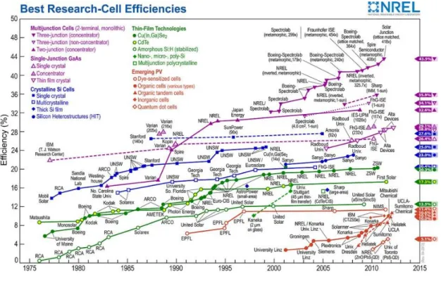
Fig. 1-1 Types of solar cells.
http://en.wikipedia.org/wiki/File:PVeff(rev100414).png
Silicon solar cell
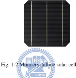
There are three major categories of silicon solar cells: single-crystal silicon,
polycrystalline silicon and amorphous silicon. At present, most of the applications are using single-crystal and polycrystalline silicon because of the following reasons: A. single-crystal silicon has the highest efficiency. B. the polysilicon technology is mature, and the price is cheaper. Most important of all, its efficiency can be competitive with the single-crystal silicon. Meanwhile, amorphous silicon has lowest
efficiency, and it can only be used in low-end products [2]. Single-crystal silicon solar cell boasts the highest efficiency in the silicon device family. The current available devices ranging from 11% to 27.6% depend on their sizes and designs. The multiple
3
crystalline device can be as high as 20.4%, and the amorphous device can be 12.5% when stacking different cells together. Even though amorphous cell is not very popular at this moment, we have to remember that its manufaturing is currently the lowest cost. If the lifetime and efficiency issues can be solved, the flexibility of amorphous silicon will be the key for its wide application.
Fig. 1-2 Monocrystalline solar cell (source: http://www.archiexpo.com)
Group II-VI material related solar cell
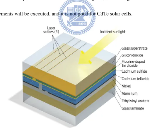
Group II-VI materials (like CdTe) with special characteristics such as good p-type conductivity and right energy band gap remain a strong contender for the advanced solar cell technology. Emission layer with n-type CdS or ZnSe, and other third group elements are usually needed to adjust the energy gap for the optimized design. In order to reduce the cost of CdTe thin films, often polycrystalline structure mainly available a variety of methods for the preparation.
4
Many designs of n-CdS/p-CdTe solar cells have been published and the highest record of power conversion efficiency can achieve 17.3%. Large area CdTe solar cell module has recently been in the mass production stage, and the energy conversion efficiency of is more than 10%, with the lifetime up to 25 years. The CdTe solar cell unit with one US dollar per watt, is the lowest-cost thin film solar cells. One of the great concerns about this technology, however, is the Cd element, which is environmentally unfriendly. In Europe, due to the environmental protection protocol, most of the hazardous material are banned from use, such as the electronic parts. The solar cell currently is not in the list. But in the long run, more stringent environmental requirements will be executed, and it is not good for CdTe solar cells.
Fig. 1-3 Cadmium telluride thin film solar cell
5 Copper-Indium Gallium Selenide
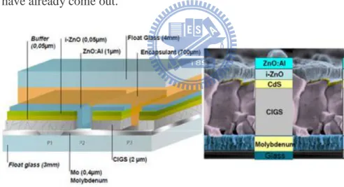
Copper Indium Gallium Selenide (CIGS) is a direct band gap semiconductor. With different combinations with ZnO (3.30eV), CdS (2.42eV), and CIS (1.02eV), high performance solar cells can be achieved. Energy conversion of CIS-based absorption layer solar cells is up to 15.4%[4], and can be as high as 20.3% in the research lab
sample.
The efficiency of CIGS solar cell module is almost comparable to silicon family. Although CIGS production technology is not mature, a small amount of production lines have already come out.
Fig. 1-4 CIGS device
(source:http://www.solarserver.com/solar-magazine/solar-energy-system-of-the-mo nth/photovoltaic-production-in-the-cigsfab-integrated-factories-provide-competitive-s
olar-electricity.html)
6
Multi-junction photovoltaic cells are composed of multiple epitaxial layers. By using different alloys of III - V semiconductors, the band gap of each layer may be adjusted to absorb the specific ranges of electromagnetic radiation from sun, but each layer must be lattice matched and each cell needs to be current-matched. These matching criteria dominate the design and performance of the current multi-junction solar cell design.
Each layer of III - V solar cells has optical absorption in series which has the highest band gap material at the top. It receives the entire spectrum in the first junction. Then top layer with a higher band gap material will first absorb the shorter wavelength (i.e. higher energy) photons, and bottom layer will absorb photons which are transmitted through the top cell.
GaAs-based devices are the most efficient multi-junction solar cells so far. By October 2010, the triple junction metamorphic cell reached a record high of 42.3%[5]
[6]
7
Fig. 1-5 Gallium arsenide multijunction solar cell
(source:http://spie.org/Images/Graphics/Newsroom/Imported-2010/003124/003124 _10_fig1.jpg)
Chapter 2 Quantum dot Ⅲ-Ⅴ solar cell
2-1 Motivation
Fossil fuels such as oil and coal nature accumulated over the years, and finally exhausted. Use too much fossil fuel emissions of carbon dioxide caused by the greenhouse effect also very worried about the future of the Earth's environment. By the semiconductor manufacturing process of solar cells can convert sunlight directly converted into electrical energy, has long been one of the great hopes of alternative energy production methods.
Currently used as a power generation of solar cells mainly Flatbed polycrystalline silicon solar cells and single crystal silicon solar cell, solar cell grade silicon material quality equal to semiconductor grade silicon, so many high-quality silicon material needs. So many high-quality silicon material requirements, use of solar energy power generation goal to become very difficult. And to produce so many of the silicon wafer must also consume a lot of energy. A feasible method is the use of concentrating technology, and use a cheap lens or mirror to focus sunlight on a small solar cell, significantly reduce the amount of solar cells. Focus on one type of solar cell power
8
generation system, the condenser the higher the magnification, and the higher the amount of conversion efficiency of solar cells used, the lower the cost of power generation.
III-V solar cell has two main aspects of concentrating solar energy power generation system with the help[7][8][9][10].
1. A higher rate of condenser: Silicon semiconductor material properties, silicon solar cell concentrator magnification is limited to about 200 times to 300 times, GaAs solar cells can be up to 1,000 times to 2,000 times.
2. Provide a higher conversion efficiency can practice: Single-crystal silicon solar cell production, 20% energy conversion efficiency is almost the upper limit, but InGaP / GaAs dual-junction solar electricity, you can reach 25 to 30%. Among the various material systems of the solar cells, the III-V solar cell has been the forerunner of the power conversion efficiency (PCE)[11]. The multiple junction tandem cell can run as high as 40% in PCE, but is still bounded by the famous Shockley-Queisser limit[12]. To break through this limit, however, requires different thoughts in the solar cell. One of the possible solutions is to use intermediate band (IB) to increase the utilization of solar spectrum. It can be shown theoretically that the single band gap material with addition of IB can convert more than 60% of received solar energy into electricity [13].
9 2-1-1 III-V solar cell
III-V semiconductor energy gap is direct bandgap. In theory, group III-V solar cell materials used in weight less and thin thickness than silicon. For the transfer of electrons and holes, thin materials only need to pass the shorter the distance you can reach the electrode, as long as the lattice of the material do not have too many defects in the natural loss of smaller, high cell efficiency. Another feature of the group III-V solar cells is the deployment of different bandgap materials, similar to the lattice dimensions of these materials can create stacked solar cell[2].
GaAs characteristics
GaAs as a direct bandgap materials at room temperature, the GaAs lattice
constant 5.6532Å band gap was 1.42 eV, its bandgap theoretically quite suitable
for the production of a single junction solar cell.
InGaP characteristics
InGaP material lattice constant match with GaAs, Ga and In, the proportion of
about 0.5:0.5 (a more precise figure is 0.51:0.49), and usually InGaP / GaAs
dual-junction solar cell, In0.5Ga0. 5P as the upper sub-solar material.
A typical Multijunction cells III-V solar cells construct the top anti-reflective layer, then the positive electrode, the top-level components for high-energy band gap of
10
GaInP, followed by the tunneling junction. Next is low band gap in the underlying
components GaAs and then finally Ge substrate. and the back electrode. GaInP lattice
constant changes by the proportion of the adjustment of In and Ga, Ga and In is about
1:1, the lattice constant is very close to the GaAs lattice, these two kinds of materials
with very good access surface at the stress and defects can be reduced to a minimum,
and is conducive to electron transfer. In addition, the Tandem Cell theoretical
efficiency with upper and lower components of the energy gap with the absolute
relationship, with a bandgap of GaInP and GaAs is quite suitable for high theoretical
efficiency[14][15].
Fig. 2-1 Lattice constant versus energy gap
http://www.tf.uni-kiel.de/matwis/amat/semitech_en/kap_2/backbone/r2_3_1.html
11 2-2-1 Physics of p-i-n solar cells
Semiconductor solar cells for an optimal design can absorb part of the conversion
of sunlight to produce voltage, current semiconductor photodetector. Semiconductor
materials absorb photons to produce electronic and electrical, combination of
semiconductor materials of different types of mixed together to form a diode, the
diode body built-in electric field will be electronic and electric separation, and in
particular the direction of current is potential difference at the p-n junction[16].
Solar cells need sunlight to work, so most of the solar cell in series with the battery,
there will be electricity generated when the sun first store to discharge to use for
non-sun. Basically, solar cells can absorb the solar spectrum energy is larger than the
semiconductor bandgap, and the amount of solar energy into electrical energy. All
electromagnetic radiation, including sunlight by photons with specific energy photons
have a wave nature, with the wavelength λ; photon energy and wavelength
corresponding relationship
hc E
(2-1) h is Planck's constant, c is the speed of light, onlygreater thanthesemiconductor material bandgapphotons to generate electron holepairs, so the solar spectrum isan important considerationinthedesignofsolar cells.
12
When the sun light shines on this P-N structure, the P type and N-type
semiconductor due to the absorption of sunlight and produce electron - hole pairs.
Due to the depletion region provided by the built-in electric field, allowing the
semiconductor electron flow within the battery, through electrode leads to the current,
we can form a complete solar cell.
Relative to the original ideal diode, solar illumination light current is a negative
current. The solar cell current - voltage relationship is the ideal diode with a negative
current to the light, that is, illumination, the solar cell is an ordinary two diode
current:
L V V s e I I I / T 1 (2-1)When the solar cell short-circuit, that is, V = 0, the short-circuit current, compared
with, that is when the solar cell short circuit, short circuit current is the incident
photocurrent, if the solar cell open circuit(open circuit), that is, I = 0, the open circuit
voltage (open-circuit voltage) was
ln 1 s L T oc I I V V (2-3)
In addition, the main applications of solar cells to convert light energy into
13
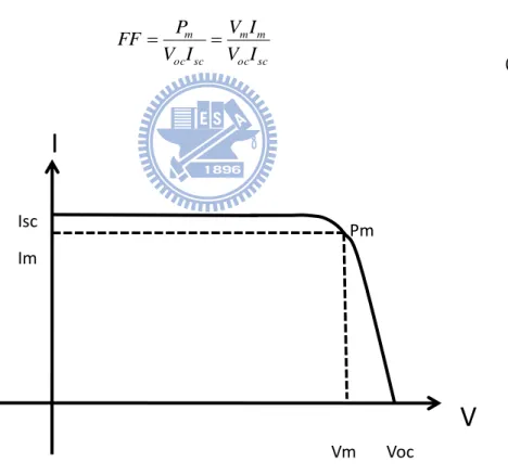
current multiplied by voltage, the former little corresponding to the voltage with
current in the current - voltage curve can be thought out a rectangle Fig.2-2, the area
of the rectangle is power, in order to facilitate analysis of solar cell device
characteristics from the current - voltage curve, in particular, the maximum power
voltage Vm and maximum power current Im shall be a rectangular area, and open
circuit voltage Voc withshort-circuit current (Isc) for the rectangular area ratio defined
fill factor, which is
oc sc m m sc oc m I V I V I V P FF (2-4)
Fig. 2-2 The solar cell IV curve
Semiconductor solar cells as an energy conversion element, most important, of course, the power conversion efficiency, output power with the ratio of the incident
I
V
Isc Im Pm Vm Voc14 power is in sc oc in m P I FFV P P (2-5)
Which the incident power Pin can measure the incident light spectrum to determine.
Semiconductor solar cells is another important parameter is the quantum efficiency as a measure of the photon conversion efficiency of the electronic, can be
divided into external electronic efficiency and internal efficiency.
The external electronic efficiency (EQE) means: a given wavelength of light
irradiation, the components can collect the maximum number of electrons and output
photocurrent with the ratio of the number of incident photons, can be expressed as
S A q I E P q I E Q E sc ph in sc / / / (2-6)Internal quantum efficiency (IQE): in a given wavelength of light irradiation, the
components can collect the output photocurrent of the maximum number of electrons
with the ratio of the number of photons absorbed, can be expressed as
1 1 1 1 / 1 / / / Wo p t ph in sc ph in sc e R m EQE T R EQE E P T R q I E P Abs q I IQE (2-7)15
transmittance; and Wopt for is the so-called optical thickness, which is equivalent to
the optical absorption length.
2-2-2 Detailed Balance Model
One of the fundamental limit on the power conversion efficiency of a solar cell was proposed by Shockley and Queisser [12]. This limit is based on detailed balance model. Detailed balance provides a technique to evaluate the maximum efficiency of photovoltaic devices under ideal situation. The calculations for detailed balance model only consider the particle flux for electrons and photons. The theory can be easily used in the analysis of solar cell designs and thus serves as the basis for our research In the following, we will follow the derivation in ref. 17 to explain the detailed balance model, and its significance towards the device physics.
There are two simplest and most common basic assumptions in detailed balance:[12][17]
1. The mobility is infinite, allowing collection of carriers no matter where they are generated.
16
Fig. 2-3 The blackbody radiancy solar spectra at 6000 K[17]
For the source of light, the blackbody spectrum is most often used in theoretical analysis. The AM0 spectrum is useful for space-based photovoltaics. The AM1.5G spectrum is often used for non-concentration solar cells while the AM1.5D spectrum is used for concentration devices[17].
Planck’s law for blackbody radiation
1 1 2 2 3 2 kT E s e c h E dE d (2-8)
represents a photon flux per unit energy flowing out of a blackbody cavity, where E is the energy, h is Planck’s constant, c is the speed of light, k is Boltzmann’s constant, and T is the temperature of the blackbody.
The sun can be treated as an ideal blackbody, so the solar energy can be summed up as:
17
g s E TT g s dE d dE E , (2-9) where Ts is the temperature of the sun. Actually, since (2-8) represents the spectral flux flowing out of the blackbody, then (2-9) represents the absorbed total flux at the sun’s surface. For a solar cell on earth, the incident solar lights are almost the same as the plane waves. Therefore the photon flux absorbed by the solar cell is actually decreased by a factor offs (2-10)
where is the solid angle subtended by the sun and the factor of 1
accounts for plane waves impingent on a planar surface. A standard value for fs is 2.1646×10⁻⁵ .
Similarly, The solar cell may be treated as an ideal blackbody at some temperature Tc.
g c E TT g c dE d dE E , (2-11) When a voltage V is applied across the device, due to the increased carrier injection, the p-n junction will see an increase in radiative recombination proportional to the Boltzmann factor, which is similar to what we saw in the forward bias current formula, and the expression for radiative recombination is thus given asc kT qV ce A U (2-12) where A is the surface area of the device and q is the elementary charge. Similarly,
18
the recombination rate due to non-radiative transitions is c kT qV e R R 0 (2-13) where R0 is the thermal generation rate. Applied to a photovoltaic device, the
principle of detailed balance implies that the sum of the overall variation of the electron-hole pair populations must be zero; thus:
Af A
A U R R
Iq q I R R U Af c c s s s s 0 0 0 (2-14) where I is the current. The term in parentheses is the net generation rate of electron hole pairs when the device is at thermal equilibrium with its surroundings. Substituting the quantity (Ac–R0) , Solving for I yields the expression for thecurrent density of the solar cell
qV kTc 1
c c c s s f e f q J (2-15) It is instructive to compare this result with the photovoltaic form of the Shockley equation: 0
1
kT qV sc I e I I (2-16) The maximum efficiency is approximately 44% for the sun with an energy gap value of 1.1 ev.19
Fig. 2-4 Efficiency versus band gap/eV
2-2-3 Intermediate band
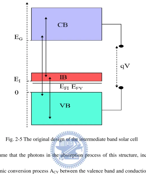
For increasing the efficiency of solar cell we add the intermediate band in the structure to absorbs additional lower energy photons, Intermediate band can be by several means like (lone pair bands, low dimensionality superlattices, quantum dots, impurities), Fig. 2-5 is the original design of the intermediate band solar cell. The traditional solar cell had only one band gap. By adding intermediate band, we can extend our absorption into longer wavelength region. In theory, the cell added intermediate band, its efficiency can exceed the Shockley and Queisser efficiency for ideal solar cells[12][13][18].
20
Fig. 2-5 The original design of the intermediate band solar cell
We assume that the photons in the absorption process of this structure, including the electronic conversion process ACV between the valence band and conduction band
electrons in the valence band and intermediate band conversion process AIV in as well
as electronic band in the middle band and conduction band between the the conversion ACI; we assume that the photons are absorbed to produce a free
electron-hole pairs the same time, the electron-hole pairs will be the opposite compound emit photons, so we will use the detailed balance deduced. Like the model of SQ of derivation, we assume that any irreversible process, the following derivation is derived under the assumption of an ideal solar cell of the following seven:
21
takes place between any two energy levels.
The ideal condition 2 (IC2): assume that the carrier has infinite mobility.
The ideal condition 3 (IC3): assume that the composition of the external current, only the conduction band of free electrons and the valence band free holes, and the middle band in any of the electron and hole flow external.
The ideal condition 4 (of IC4): assume that the battery is thick enough to absorb all the incident photons, in order to ensure that all three conversion process will occur. The ideal condition 5 (IC5): assume that the bottom of the battery or other locations are set to have a perfect mirror to ensure that the photon escaping from the battery to the front area.
The ideal condition 6 (of IC6): Suppose that in any photon energy range, only a photoelectric conversion process will occur.
The ideal condition 7 (IC7): assume that the light in the isotropic within the battery. As shown, we assume that the three quasi-Fermi levels were ∈FC, ∈ FI, and ∈ FV the
battery chemical potential μCV in = the the ∈FC-∈FV, the μCI = ∈FC,-∈ FI, μIV = ∈FI- ∈FV;
set the energy gap between the energy gap between the conduction band and valence band is set to ∈G, the conduction band and intermediate band ∈C, the energy gap
between the intermediate band and the valence band is set to ∈I, andlocated ∈I <∈C,
22
modes:
1. ∈ <∈ I: no photon is absorbed.
2. When ∈I <∈ <∈C: the photon is absorbed and lead to the transition between
the electron and hole in the middle of the band and the valence band.
3. When and ∈C <∈ <∈G: photons are absorbed and lead to electron-hole
interband transitions in the conduction band and the middle
4. ∈G <∈: the photon is absorbed and lead to electron and hole in the
conduction band and valence interband transitions.
Assume that the cell has a maximum condenser 46000 times, the incident photons and emit the photon flux will meet the following thermodynamic equation [3]:
(2-17) Where T is temperature, c is the speed of light, h is Planck's constant, μ is the chemical potential; μ set to 0 and T is set to sun the temperature TS, you can get the
incident photon flux . Then we can get the flow to the external current conduction band to meet the following formula:
(2-18) Output current in an external potential difference is equal to the conduction band and valence band between the Fermi gradient qV = μCV = μCI + μIV. In the absence of
23
any current outflow from the middle band, so you can launch the current conservation equation:
( 2 - 1 9 )
calculate the maximum power divided by the incident radiant power
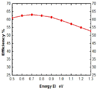
(σ is the Boltzmann constant) can be the theoretical maximum efficiency. Calculation results shown in Fig. 2-6, calculated in arbitrary ∈I, ∈G maximum
efficiency corresponds to the intermediate band, perfect backlit mirror and the largest condenser the theoretical maximum efficiency) curve; results showed that with the middle of the band structure of photoelectric conversion efficiency can reach 63.1%, 40.7% higher than that of SQ the model calculation results.
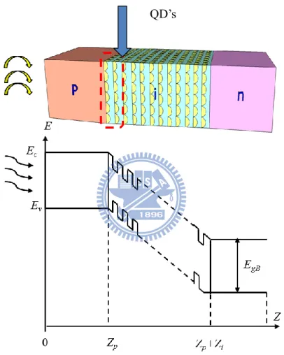
24 2-2-5 Quantum Dot Solar Cell
We can divide the photocurrent into three sections, where the first and second are current generated from n and p-type regions and the final is current generated from QD’s structure. For one thing, at the p-type region, we can define the scope is extended from Z=0 to Z=Zp.
Fig. 2-7 Schematic structure of energy-band diagram of p – i – n QD solar cell. Because of the standard equations for electron current density and electron continuity, we can figure out the distribution of minority carriers and obtain the electron–hole generation rate [18].
Gp
,z
1 R
F
e x p
z
(2-20)25
Which is under room temperature situation and where R(λ) is the surface reflection coefficient and a(λ) is the light absorption coefficient of GaAs. For overall understanding, we should find out the inconvenient part of solar flux F(λ). In this we make use of the model of solar spectrum described by a black body curve at the temperature of 5760 K, and acquire that
1 2 , 1 4 21 1 exp 10 5 . 3 m s cm photon kT hc F (2-21) where h is the Plack’s constant, c is the velocity of light, k is the Boltzmann’s constant, and T1=5760K.
To follow we induce continuity equation since the excess electrons.
, 0 2 2 n p D z G Ln z n dz z n d (2-22) where Ln and Dn are the electron diffusion length and diffusion constant,
respectively. Furthermore, owning to there is no bias voltage, we learn that the generation current only in proportion to the Dn=ә△n(x)/әx section . On account of the boundary conditions we can obtain
0 0 n S dz n d D n z n (2-23)
Finally, by solving the continuity equation we have
n p n n n p n n n n p n n n n n n L z a b L z a b L a z a b a a R eF j sinh 1 cosh( exp 1 1 2 (2-24) Where e is the electronic charge,
1sinh cosh p n n p n n z L b z L , bnSnLn Dnand n n a L
a , the total photocurrent collected by p-type region is equal to
1 0 d j Jp n n (2-25)26
where λ1 is the absorption cut-off wavelength. Similarly, we can obtain the
photocurrent of the intrinsic and n-type region by the same derivation. The final short-circuit current Jsc can be written as:
Jsc=fi(Jn p
+Jp n
+Ji) (2-26)
The results obtained from equations (2-20) to (2-23) are generic and no quantum dots effects are considered. To properly include the contribution from quantum dots, we have to modify several things. First, the carriers generated from bulk GaAs and quantum dots can be calculated separately using similar concept in equation (2-20) to (2-23). However, when we consider the summation of all currents and the solar cell circuit model, the ordinary current-voltage relation: J=Jsc-J0[exp(eV/kT)-1], needs to
be changed. The saturation current J0 can be divided into two components: one from the edge of depletion layers (js,bulk), and the other from interior of depletion
region(js,QD) [19]. By detailed balance between the radiation and thermal equilibrium,
these components can be written in the form of: [19][20]
kT E A
jseff edd geff
,
, exp
(2-27) where Aeff is a constant proportional to Eg,eff2,and Eg,eff is the effective band gap
defined by percentage of i-region volume occupied by quantum dots (denoted by P): Eg,eff=(1-P)×Eg,bulk+P×Eg,QD. For the bulk case, the Aeff and Eg,eff(=Eg,GaAs) can be
27
js,QD. With J0 changed due to quantum dots, we can calculate the I-V (or J-V)
characteristics of a quantum dot device more accurately. Second, the spectral absorption line shape of quantum dot needs to be considered when we model the generation rate G(λ,z) in equation (2-20). The shape of absorption of quantum dot can directly affect the photo-generated currents and thus the efficiency of the solar cell. In the ideal case, the quantum dot absorption is a delta function located at the discretized levels. However, in practical case, the quantum dot absorption is broadened by the non-homogenous size distribution of the dots, and imperfect of the material. The Fig. 2-8 shows our simulation on the single junction device in the ref. [22],
(a) (b) (c)
Fig 2-8. QD layer thickness and QD volume density impact to (a)Jsc (b) Voc(C) efficiency[19]
The shape of absorption of quantum dot can directly effect the photo-generated currents and thus the efficiency of the solar cell. In the ideal case, the quantum dot absorption is a delta function located at the quantum dot discretized levels. However,
28
in practical case, the quantum dot absorption is broadened by the non-homogenous size of the dots, and imperfect of the material. Usually a Lorentzian line shape is used
[22]
.
2-2-4Tunnel Junction
The wide bandgap tunnel junction connecting the InGaP and GaAs two sub-solar and avoid absorbing too many photon of the GaAs solar cell photon need. A
tunnel junction is a simple p + + / n + + junction where the p + + or n + + material in high
doping concentrations, has reached the degenerate state. The relationship with A tunnel junction tunneling current density Jp and the bandgap reference doping
concentration is[23] * 2 3 exp N E Jp g (2-28)
Eg is able to band gap, N * = NAND / (NA + ND) is dimensional equivalent doping
concentration. The maximum tunneling current density Jp must more than
solar-generated photocurrent, otherwise it will seriously reduce the solar cell
conversion efficiency.
2-2-5Tandem Cell
29
bandgap solar cell to achieve the best structural design of the absorption efficiency. By the theoretical calculation, if there are more number of layers in the structure, the cell efficiency will be increased gradually, and can even reach 50% conversion efficiency[16].
Fig. 2-9 Use dichroic mirror to separate the spectrum to allow other cell absorption[16]
In fact, the effective to separate the spectrum as shown in Fig. 2-9 is difficult to achieve. So in reality, we use the variety of different band gap semiconductor
materials to stack the cell, and the wide energy gap of the material stacked on the top
of the solar cell to absorb higher energy photons, while the low energy photons will
be absorbed by smaller band gap material. It can be optimized to produce the
I
I
I
IR
red
blue
small E
gcell
intermediate E
gcell
30
greatest efficiency from the independent design of the different junction[24][25].
We use the two available energy gap Eg1 and Eg2, respectively bottom and top
the cell to calculate the available power. Assuming that the solar spectrum can be
perfectly separated, and all the photon energy E> Eg2 of the top cell will be
completely absorption, while the photon energy Eg1 <E <Eg2 is absorb by bottom cell,
we can get the maximum power output
2 2 2
2 1 2 1 2 1 1 m a x , , , 0 , , , , , , 0 , , , m a g s g m m a g g s g g m qV T E N T E N qV qV T E E N T E E N qV P (2-29)While where the Vm1 and Vm2 are respectively to generate maximum power for the
top cell voltage and the bottom cell voltage. In the Pmax equation the two bias can be
independently optimized.
pm a xq
V1V2
N
Eg1Eg2, Ts,
,0N Eg1E,g2 ,Ts,qV1
(2-30)Where V1 and V2 are no longer representative of the individual cell voltage, but to
meet the constraints current Pmax under stable conditions
N Eg1,Eg2,Ts,0 N Eg1,Eg2,Ts,qV1
N
Eg1,,Ts,0
N Eg2,,Ta,qV2
( 2 - 3 1 )When Pmax in stable conditions, the efficiency is smaller, the impact of energy band
31
Reduce heating losses, at the same time, improve the absorption efficiency to provide a solar cell in a narrow photon energy interval Eg< <E g+dE, and the other
photon of solar cells with different band gap.
For blackbody solar spectrum, solar cell energy gap Eg and idealized absorption
rate of a( <E g)=0,a( E g)=1, short-circuit current is
d kT c e j g E s s sc
1 exp 4 2 2 3 3 (2-32)From Fig. 2-10 the shadow rectangle in thermal equilibrium, we can see jE, eh
energy transfer to the maximum value of electron-hole pairs[23].
Fig. 2-10 jsc with Eg diagram, Ts = 5800K[23]
32
jE,eh jscEg/e j,absEg (2-33)
The Eg+3kT replaced (Ee+Eh)=Eg, we divided the overall efficiency of η is slightly
different (and not entirely correct) into the thermal and thermodynamic efficiency,
jsc(Eg/e) the area under the entire incident energy current je,sun from the sun. This can
see if we determine that the of the variation djsc, the short-circuit current changes dEg
absorption in the band gap. g s g g s sc dE kT E E c e dj 1 exp 4 2 2 3 3 (2-34)
Integral the variables -(Eg/e)djsc, we can get
g s g g s sc g E dE kT E E c dj e E dj
0 3 2 3 3 0 1 exp 4 (2-35)This formula can be seen the relationship between short-circuit current and the energy gap,
33
Fig. 2-11 The two energy gaps, respectively Eg1=1.8eV,Eg2 =0.98eVof the solar
cellcurrent- voltageproperties[23]
Fig. 2-11 For two solar cells with different can the gap Eg1 and Eg2, exposure the
light intensity for the AM0 spectrum, when the energy greater than the energy gap Eg1,
all photon in <E g1 is absorbed by first cell. remaining transmission had to know
all the photon energy in Eg1 energy for Eg2 << Eg1, is at the bottom of the second cell
absorption to produce a larger current and improve efficiency.
The remaining transmission over the photon energy is smaller than Eg1. And energy
with Eg2< <E g1, is absorb by the bottom of second cell to produce a larger current
34
Chapter 3 Simulation and Results Discuss
In this section, we will demonstrate our simulation results by combining the aforementioned theories and models. We built our device model by using Matlab® coding, commercial software Silvaco® and APSYS®. A proper inclusion of quantum-dot-related carrier absorption is adapted through modified extinction coefficient k, and effective band gap of the device. The final calculation shows good agreement to measurement. This platform has great potential to analyze novel photovoltaic devices.
3-1 Simulation software
Next, I will give a brief introduction for the software I use to calculate the structure.
3-1-1 Silvaco®
We used software is called TCAD® by corporation Silvaco® and use the modular Atlas® to do device simulation. ATLAS provides general capabilities for physically-based two (2D) and three-dimensional (3D) simulation of semiconductor devices. ATLAS is a physically-based device simulator. There are three basic semiconductor equations to solve the device calculation. There are: Poisson’s equation, carrier continuity Equations, the transport Equations [26].
35
3-1-2 Matlab®
MATLAB® is a programming environment for algorithm development, data analysis, visualization, and numerical computation. Using MATLAB®, you can solve technical computing problems faster than with traditional programming languages. In my simulation, I use the 2-2-5 Quantum Dot Solar Cell I mentioned formula to calculate the structure[27].
3-1-3 APSYS®
APSYS® is a general purpose 2D/3D modeling software program for semiconductor devices. Based on finite element analysis, it includes many advanced physical models. APSYS® offers a very flexible and simulation environment for modern semiconductor devices. The variety of physical phenomena in a semiconductor require many different physical models. However, Poisson’s equation, carrier continuity equations, the transport equations are the most basic since many of the well known characteristics of a semiconductor device[28].
3-2 Simulated structure
3-2-1 Single junction solar cell
First, we use the scheduling function of VWF Silvaco® simulation software to identify most of the material added thickness and doping concentration. VWF can
36
carry out experiments, where a chosen optimization algorithm is used to vary split parameters so that a defined target is minimized[26].
(a) (b)
Fig. 3-1 Optimization of the solar cell (a) GaAs single cell (b) InGaP single cell
The structure of the solar cell is composed of GaAs /InGaP materials. After optimization of the design, we find out that the structures of the GaAs cell and InGaP solar cells shows in Fig. 3-2
(a) (b) Fig.3-2 The optimize structure of single cells (a)InGaP cell (b) GaAs cell
37
Calculation of the use of Silvaco® software, we designed the structure the jsc of
InGaP is 9.69 mA/cm2 and voc of InGaP is 1.32 V; the jsc of GaAs is 23.21 mA/cm2
and voc of GaAs is 0.92 V. Then we use the other two software which are Matlab
®
and APSYS® to campare the calculation result in Fig 3-3. We can see that the calculated results are quite similar.
38
Fig.3-3 Calculated EQE / IV characteristics of InGaP and GaAs solar cell by softwares (a)and(c) EQE versus wavelength (b)and (d) IV curves.
3-2-2 Solar cell with quantum dots
This chapter, we added quantum dots GaAs solar cells we design (as shown in Fig 3-4) . First of all, we used the simulation software APSYS® to calculated the quantum dot same thickness but the density is not the same, on the solar cell affect.
39
40
Fig 3-5. The different density of quantum dots on GaAs solar cell calculated by APSYS®(a) EQE versus wavelengthand (b) IV curves.
GaAs cell is added to the quantum dots, EQE shows different quantum efficiency, but
41
Fig. 3-6 The different percentage of quantum dots in the i-layer of GaAs solar cell APSYS® [(a) and (b)] ,and Silvaco® [(c) and (d)]
By Fig. 3-6 can be seen, in APSYS calculation, the higher the percentage of quantum dots in the i region and EQE in a long wavelength pick more obvious, but the efficiency, current density and voc are decreased. In Silvaco the calculation under,
42
Cause the QD different percentages in the i layer EQE considerable confusion.
Then we will use the the simulation software silvaco to do simulate different wavelength absorption quantum dots (as shown in Fig 3-7) in GaAs solar cells i region to know the impact of the cell.
43
Fig. 3-8 Different QDs wavelength absorption in solar cell calculated by Silvaco (a) EQE versus wavelength (b) IV curves
Under in simulation software silvaco calculation, we can see that in the quantum dots in the different position of absorption, the current-voltage characteristic of the solar cell does not impact (as shown in Fig. 3-8).
Next use the software Silvaco® to simulation the different intensities of quantum dots absorption (I call test 56 in my research) in GaAs solar cell.
44
45
Fig. 3-10 different QDs intensities in solar cell calculated by Silvaco (a) EQE versus wavelength (b) IV curves
Under in simulation software Silvaco® calculated, by Fig. 3-10 seen, when the increase in the intensity of the absorption of the quantum dots, the current density will rise, but under in silvaco calculation, the increase in the absorption intensity of the quantum dots in the open-circuit voltage does not affect.
Next we compare the measured data to our calculation. A single junction AlGaAs/GaAs/InAs QD solar cell device (shown in Fig. 3-11)[29]
46
Fig. 3-11 The schematic diagram of a single junction InAs-QD solar cell.
(a) (b)
47
48
Fig. 3-13 Comparison of calculated and measured EQE / IV characteristics of GaAs solar cell with QD by Silvaco® [(a) and (b) with QD×3] ,[(c) and (d) with QD×5]
49
Table 3-1 Simulated in Silvaco® and measured values
Device
type
Jsc (mA/cm2) Voc (V)
Measurement Calculation Measurement Calculation
QD*3 8.5 8.6 0.72 0.72
51
Fig. 3-14 Comparison of calculated and measured EQE / IV characteristics of GaAs solar cell with QD byMatlab® [(a) and (b) with QD×3] ,[(c) and (d) with QD×5]
Table 3-2 Simulated in Matlab® and measured values
Device
type
Jsc (mA/cm2) Voc (V)
Measurement Calculation Measurement Calculation
QD*3 8.5 8.3 0.72 0.72
QD*5 8.4 8.4 0.57 0.57
We use Silvaco and Matlab to simulate the structure with different layers of quantum dot which were QDx3, QDx5, and the one QD layer's thinkness was 0.01um.
52
Fig. 3-11 shows our device layer design, and Fig. 3-12 the band diagram from the software. The quantum dot layer is based on GaAs material parameters but also adapt the quantum dot absorption spectral line shape in [20]. And then we use our simulation result to compare with the measurement data. In the Fig. 3-13 to Fig. 3-14 different layers of QD were placed in the ordinary GaAs solar cell structure, and their EQE and IV were calculated. We put lots of emphasis in the fitting of wavelength dependent EQE and try to match the IV as well. From the results, we can see that the EQE with longer wavelength absorption was successfully fitted.
3-2-3 Dual junction solar cell
Reference 3-2-1 single junction solar cell design out of a solar cell data and various data related papers, we Use the tunnel junction to connection GaAs solar cells and InGaP solar cells for tandem cell[30][31].
Fig. 3-15 Optimization of the InGaP/GaAs tandem cell calculated by Silvaco® After we use the tunnel junction to connect the two single cells,we use the VWF in software to optimize the thickness of the best tandem cell. As the Fig. 3-15 shown, we
53
can see when i region of InGaP cell in 0.5 µm and i region in GaAs cell in 1 µm has the maximum efficiency.
54
Fig. 3-16 IV curve of tandem cell simulated by three software (a) Matlab® (b) Silvaco® (c) APSYS®
55
Fig. 3-17 EQE vurses wavelength of tandem cell simulated by three software (a) Matlab® (b) Silvaco® (c) APSYS®
Use of three different software simulation the tandem cell structure I design, we can see three software calculation results are quite close.
56
3-2-4 Dual junction solar cell with quantum dots
InGaP p-i-n
top cell
GaAs p-i-n
bottom cell
InGaAs QDs
GaAs Substrate
Tunnel Junction
InGaP p-i-n
top cell
GaAs p-i-n
bottom cell
InGaAs QDs
GaAs Substrate
Tunnel Junction
InGaP p-i-n
top cell
GaAs p-i-n
bottom cell
InGaAs QDs
GaAs Substrate
Tunnel Junction
Fig. 3-18 InGaP/GaAs QD tandem solar cell schematic diagram
After we achieve a good fitting on the single junction InAs QD cell and good simulation of tandem cell, we can move onto a more complicated design. As shown in Fig. 3-18, a dual junction InGaP/GaAs+InAs QD is a good candidate for high efficiency devices. In our simulation, we have two types of devices to be demonstrated, one is using structure which is close to what other people implemented, and the other is the ideal device with 100% quantum efficiency[32]. Fig.3-19 shows the generic result of EQE and IV calculation from ordinary structure.
58
Fig. 3-19 Calculated EQE / IV characteristics of Tandem solar cell with QD by Matlab®[(a) and (c)], and Silvaco® [(b) and (d)]
The QD absorption is marked at the longer wavelength band (> 880nm). With full current-voltage characteristics obtained, the final PCE can be found as well. In Fig. 3-20, we calculated power conversion efficiency (PCE) versus the percentage of
59
quantum dot volume in the intrinsic region with three different designs: the bottom two curves are practical structures, and the top one is the ideal cell result. From the calculation, several observations can be deducted: first, the ideal enhancement brought by quantum dot can be estimated to 11% at most, which is consistent with our detailed balance model [33].
Second, if we use the structures published in most papers, the efficiency tends to drop when QD layer is added (as the green curve in Fig. 3-20), and only when we increase the intrinsic region
thickness to ensure at least 90% quantum efficiency, the addition of QD layer is beneficial (the blue curve in Fig. 3-20). Third, we found there are knee-like features in the plot (like in ideal case), which is rising from the crisscross of the shortcircuit current between the top and bottom cells.
Fig. 3-20 Efficiency vs. percentage of QD volume in the intrinsic region calculated by Matlab®.
60
From our calculation, we found that in most of the cases, the QD devices generate inferior PCE compared to pure GaAs/InGaP tandem cells. Although this is not very encouraging, they do agree with most of the experimental data so far [34]. The calculation makes the authors to believe that the utilization of the photon in the cell has to be nearly perfect for QD layer to be useful. As we see in the ideal case, a perfect quality of the material growth will be required for IBSC device to outperform the ordinary device.
61
Chapter 4. Summary& future work
We demonstrate Silvaco®, Matlab® and model to calculate the GaAs solar cell with quantum dot. . The calculation was carried out by Matlab®, Silvaco TCAD® and APSYS® software for the analysis purpose. The final results show a very good match between measurement and calculation
We propose a novel design by combining the merits of IBSC and multiple junction tandem cell. This idea was carried out by a Matlab® and Silvaco® platform for the numerical study. The final results show an efficiency as high as 34.5% can be achieved.
Future research, I have to strengthen the simulation software APSYS®calculation research, hope to add quantum dots in daul junction solar cell, expect to design more high efficient solar cells.
62
Reference
1. Z. Q. Li, Y. G. Xiao, Z. M. Simon Li, Proc. of SPIE, 6339. (2006) 633909 2. 黃惠良,蕭錫鍊,周明奇,林堅楊,江雨龍,曾百亨,李威儀,李世昌,林唯方”太陽能
電池”五南圖書出版公司
3. X. Wu, R.G. Dhere, D.S. Albin, T.A. Gessert, C. DeHart, J.C. Keane, A. Duda, T.J. Coutts, S. Asher, D.H. Levi, H.R. Moutinho, Y. Yan, T. Moriarty, S. Johnston, K. Emery, andP. Sheldon, NREL/CP-520-31025 (2001).
4. B. J. Stanbery, Critical Reviews in Solid State and Materials Sciences 27 (2002) 73.
5. Martin A. Green1*, Keith Emery2, Yoshihiro Hishikawa, Wilhelm Warta and Ewan D. Dunlop, Prog. Photovolt: Res. Appl. 20 (2012) 12
6. D. J. Friedman, S. R. Kurtz, K. A. Bertness, A. E. Kibbler, C. Kramer, and J. M. Olson, Phot. Ener. Conv. 2 (1994) 1829.
7. T. J. Coutts, J. S. Ward, D. L. Young, K. A. Emery, T. A. Gessert and Rommel Noufi, Prog. Photovolt: Res. Appl. 11 (2003) 359.
8. J. W. Leem · Y. T. Lee · J. S. Yu, Opt Quant Electron 41 (2009) 605.
9. Y. Bai, Y. Cao, J. Zhang, M. Wang, R. Li, P. Wang, S. M. Zakeeruddin and M. Grätzel, Nature Materials 7 (2008) 626.
10. Y. Hashimoto, US Patent 4,963,196, 1990.
11. W. Guter, J. Schone, S. P. Philipps, M. Steiner, G. Siefer, A.Wekkeli, E. Welser, E. Oliva, A. W. Bett, and F. Dimroth, Appl. Phys. Lett. 94 (2009) 223504
12. W. Shockley, H. J. Queisser, J. Appl. Phys.32 (1961) 510 13. A. Luque, A. Martı, Phys. Rev. Lett. 78 (1997) 5014
14. K. A. Bertness, Sarah R. Kurtz, D. J. Friedman, A. E. Kibbler,C. Kramer, and J. M. Olson, Appl. Phys. Lett. (1994) 65
15. T. Takamoto, E. Ikeda, and H. Kurita, Appl. Phys. Lett. 70 (1997) 381
16. Jenny Nelson,’’Physics of Solaar Cells,’’ Imperial College Press ISBN 1-86094-340-3, (2003).
17. R. Aguinaldo, “Modeling Solutions and Simulations for Advanced III-V Photovoltaics Based on Nanostructures”, Center for Materials Science & Engineering College of Science Rochester Institute of Technology Rochester, NY
63
December 2008
18. A. Luque and A. Martı´, Advanced Materials, 22 (2010). 160
19. V. Aroutiounian, S. Petrosyan, A. Khachatryan, and K. Touryan,“Quantum dot solar cells”, J. Appl. Phys. 89 (2001) 2268.
20. C. H. Henry, J. Appl. Phys. 51 (1980) 4494.
21. S. M. Sze, "Physics of Semiconductor Devices," John Wiley & Sons, New York, Ch. 2, 2nd Edition, 1981.
22. S. L. Chuang, “Physics of Photonic Devices”, Chapter 9, John Wiley & Sons Inc., (2009).
23. Peter Wurfel,”Physics of Solar cells From Principles to New Concepts” 2005 WILEY Vcrlag GmbH& Co, KGaA, Weinheim
24. M. A. Cusack, P. R. Briddon, and M. Jaros, Phys. Rev. B, 56 (1997) 4047. 25. T. Takamoto, E. Ikeda, H. Kurita, and M. Ohmori Appl. Phys. Lett. 56 (1990) 623 26. ATLAS User’s Manual, Chapter 3, 2009, Silvaco, Santa Clara,CA.
27. http://www.mathworks.com/products/matlab/
28. Crosslight Device Simulation Software-General Manual 20111995-2010 Crosslight Software Inc.
29. K.Y. Chuang, T.E. Tzeng, Y.C. Liu, K.D. Tzeng and T.S. Lay, J. Crys. Grow. 323 (2011) 508
30. J. F. Geisz, S. Kurtz, M. W. Wanlass, J. S. Ward, A. Duda, D. J. Friedman, J. M. Olson, W. E. McMahon, T. E. Moriarty, and J. T. Kiehl, Appl. Phys. Lett. 91 (2007) 023502
31. M. Yamaguchia, T. Takamotob, K. Araki, Solar Energy Materials and Solar Cells 90 (2006) 3068.
32. S. Tomić, Phys. Rev. B 82 (2010) 195321.
33. C. C. Lin, W. L. Liu and C. Y. Shih., Opt. Express, 19 (2011) 16927
34. C. G. Bailey, D. V. Forbes, R. P. Raffaelle, and S. M. Hubbard, Appl. Phys. Lett.. 98 (2011) 163105.
![Fig 2-8. QD layer thickness and QD volume density impact to (a)Jsc (b) Voc(C) efficiency [19]](https://thumb-ap.123doks.com/thumbv2/9libinfo/8751624.206055/37.892.134.761.555.863/fig-layer-thickness-volume-density-impact-jsc-efficiency.webp)
![Fig. 2-9 Use dichroic mirror to separate the spectrum to allow other cell absorption [16]](https://thumb-ap.123doks.com/thumbv2/9libinfo/8751624.206055/39.892.152.779.337.737/fig-use-dichroic-mirror-separate-spectrum-allow-absorption.webp)
