Alkylation of nanoporous silica thin films by high density plasma chemical vapor
deposition of a- SiC:H
F. M. Pan, B. W. Wu, A. T. Cho, K. C. Tsai, T. G. Tsai, K. J. Chao, J. Y. Chen, and L. Chang
Citation: Journal of Vacuum Science & Technology B 22, 1067 (2004); doi: 10.1116/1.1738668
View online: http://dx.doi.org/10.1116/1.1738668
View Table of Contents: http://scitation.aip.org/content/avs/journal/jvstb/22/3?ver=pdfcov Published by the AVS: Science & Technology of Materials, Interfaces, and Processing
Articles you may be interested in
Origin and effect of impurity incorporation in plasma-enhanced ZrO 2 deposition J. Appl. Phys. 93, 9345 (2003); 10.1063/1.1572193
Effect of N 2 O plasma treatment on the stabilization of water absorption in fluorinated silicon-oxide thin films fabricated by electron-cyclotron-resonance plasma-enhanced chemical-vapor deposition
Appl. Phys. Lett. 80, 1728 (2002); 10.1063/1.1458528
Characteristics of fluorinated amorphous carbon films and implementation of 0.15 m Cu /a- C:F damascene interconnection
J. Vac. Sci. Technol. B 19, 780 (2001); 10.1116/1.1362683
Patterning of fluorine-, hydrogen-, and carbon-containing SiO 2 -like low dielectric constant materials in high-density fluorocarbon plasmas: Comparison with SiO 2
J. Vac. Sci. Technol. A 17, 741 (1999); 10.1116/1.581643
Some characteristics of wide gap a- SiC:H films deposited by electron cyclotron resonance chemical vapor deposition using acetylene
vapor deposition of
a
-SiC:H
F. M. Pana)Department of Materials Science and Engineering, National Chiao Tung University, Hsinchu 300, Taiwan, Republic of China and National Nano Device Laboratories, Hsinchu 300, Taiwan, Republic of China
B. W. Wu, A. T. Cho, K. C. Tsai, and T. G. Tsai
National Nano Device Laboratories, Hsinchu 300, Taiwan, Republic of China K. J. Chao
Department of Chemistry, National Tsinghau University, Hsinchu 300, Taiwan, Republic of China J. Y. Chen and L. Chang
Department of Materials Science and Engineering, National Chiao Tung University, Hsinchu 300, Taiwan, Republic of China
共Received 10 October 2003; accepted 14 March 2004; published 11 May 2004兲
Film stacks of a-SiC:H and molecularly templated nanoporous silica thin films have been prepared, and alkylation of pore surfaces of the nanoporous silica layer by the a-SiC:H layer was studied. The a-SiC:H thin films were deposited by high-density plasma chemical vapor deposition共HDP-CVD兲 using trimethylsilane 共3MS兲 as the precursor. Carbon is found to uniformly distribute in the thin nanoporous silica film, and the carbon content in the nanoporous film decreases with increasing the a-SiC:H deposition temperature. We used the modified Sanderson formalism to estimate the corresponding Si(2 p) and C(1s) electron energies in x-ray photoelectron spectra共XPS兲 for possible terminal species on pore surfaces in the nanoporous silica layer. According to the XPS analysis and thermal desorption mass spectroscopy, the terminal species are probably in the chemical form of alkoxyl structures. The alkoxyl terminal groups introduced into the nanoporous silica thin film are believed to stem from hydrocarbons trapped in microvoids in the a-SiC:H film, which are formed during the HDP-CVD deposition. The terminal alkoxyl groups in the nanoporous silica layer can greatly enhance the hydrophobicity of the nanoporous silica dielectric, and hence improve the dielectric property of the film stack of a-SiC:H/nanoporous silica. An effective dielectric constant smaller than 1.7 can be obtained for the film stacks. © 2004 American Vacuum Society.
关DOI: 10.1116/1.1738668兴
I. INTRODUCTION
Nanoporous silica dielectric materials are widely recog-nized as a potential candidate for intermetal dielectric layer for sub-100 nm integrated circuit 共IC兲 technologies because of their ultralow dielectric constants and chemical compat-ibility with contemporary IC process technologies. Molecu-larly templated nanoporous silica dielectrics have received extensive attention since the first discovery of hexagonally ordered MCM-41 in 1992.1–3 By selecting an appropriate template molecule, the templated nanoporous films have an extremely high porosity and a uniform pore size distribution, leading to a very low k value and a better mechanical prop-erty compared with other porous materials.4 However, nan-oporous silica films are liable to moisture uptake, and cannot be directly implemented in IC processes before any hydro-phobicity treatment. To improve the hydrohydro-phobicity, nanopo-rous silica thin films are usually treated with hexamethyl-disilazane共HMDS兲 vapor for trimethylsilylation on the pore surface, and thus the dielectric property of the nanoporous films can be greatly improved as well. With further hydrogen
plasma treatments, the dielectric constant of HMDS modified nanoporous silica films can be reduced to a value below 1.5.5,6
Hydrogenated amorphous silicon carbide (a-SiC:H) is an interesting material in terms of optical, electrical, and me-chanical properties. It has a wide range of optical band gap depending on the chemical structure, in particular the atomic ratio of silicon to carbon.7Recently, it has been used as the dielectric barrier layer because it has mechanical and chemi-cal features, such as toughness and chemichemi-cal resistance, simi-lar to crystalline silicon carbide, while at the same time it has a relatively low dielectric constant compared with silicon nitride.8 Trimethylsilane 共3MS兲, (CH3)3 SiH, is a
nonpyro-phoric organosilicon gas, and can be used as the gas source to deposit a-SiC:H dielectric thin films in a standard plasma chemical vapor deposition systems. In addition to its high mechanical strength and chemical resistance, the 3MS based a-SiC:H film typically has a slower etch rate than plasma deposited silicon nitrides using a standard fluorocarbon-based etching gas source.9This becomes a very useful char-acter when a-SiC:H films are implemented in dual-damascene processes as the dielectric barrier or etch stop layer because of the high etch selectivity of the carbide to the
silica dielectric. Since a large quantity of terminating hydro-gen and methyl groups are present in the silicon carbide net-work, many microvoids are present in a-SiC:H films depos-ited at low temperatures. However, at high deposition temperatures (⬎350 °C), decomposition of hydrogen and methyl groups enhances network crosslinking and results in a denser film. Due to these microvoids, the a-SiC:H film, when used as a barrier layer or etch stop layer in damascene processes, will certainly exhibit some process characteristics much different from those conventional dielectric materials, such as silicon nitride.
In the study, we have deposited an a-SiC:H layer in con-junction with molecularly templated nanoporous silica thin film by high-density plasma chemical vapor deposition 共CVD兲 method using 3MS as the precursor. The HDP-CVD film can behave as a diffusion source providing hydro-carbon gases to the nanoporous silica thin film, thereby en-hancing the hydrophobicity of the nanoporous silica dielectric layer. This can greatly improve the dielectric prop-erty of the intermetal dielectric layer. In addition, when sand-wiched by two nanoporous silica layers, the a-SiC:H film can be used as an etch stop layer or barrier layer in a dual-damascene interconnect structure.
II. EXPERIMENT
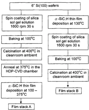
Two film stack structures were fabricated on Si共100兲 wa-fers in the study. One film stack consists of the a-SiC:H film deposited on the spin-coated nanoporous silica thin film 共stack A兲, and the other film stack has a nanoporous silica film deposited on the HDP-CVD a-SiC:H thin film 共stack B兲. The a-SiC:H film is deposited by an inductively coupled plasma HDP-CVD system. Figure 1 shows the preparation scheme of the a-SiC:H/nanoporous silica film stack. A mix-ture of tetraethyl orthosilicate共TEOS兲, Pluronic p123, H2O,
HCl, and ethanol was refluxed at 70 °C for 90 min in the molar ratios: 1:0.03:4:0.03:34. Pluronic p123, a triblock co-polymer, was used as the template molecule. The solution mixture was aged for 3– 6 h at room temperature, and then the aged solution was spin-coated on a 4 in. p-type Si wafer in the clean room. After spin-coating, the nanoporous silica film was kept at 100 °C for 30 min to remove solvent, fol-lowed by a calcination treatment at 400 °C. For film stack A, the nanoporous silica layer was annealed at 375 °C in the HDP-CVD system for 1 h to remove adsorbed moisture right before the a-SiC:H deposition. The a-SiC:H film deposition was carried out at various substrate temperatures with a 3MS flow rate of 20 sccm at 1–10 mTorr and a plasma power of 300 W. For film stack B, the a-SiC:H film was directly de-posited on the silicon wafer at 130 °C under the same plasma condition as stack A. The nanoporous film was then prepared on the a-SiC:H layer in the clean room ambient followed by calcination at 400 °C for 1 h. According to previous studies,5 the porosity and the pore size of the nanoporous silica in this study were around 50% and 40 Å, respectively. The thick-ness of a-SiC:H films varied depending on the deposition condition, such as the substrate temperature and the stack
structure, but all the films discussed thereafter were all thin-ner than 30 nm. The thickness of the nanoporous silica film was around 250 nm.
Metal-insulator-semiconductor capacitor test structures were fabricated in order to study the dielectric property of the a-SiC:H/nanoporous silica film stack. The capacitance of the film stacks was measured with a Keithley CV meter 共Model 590兲 at 1 MHz, and the leakage current was mea-sured by an HP 4156A semiconductor parameter analyzer. Fourier transformed infrared spectroscopy 共FTIR兲, Auger electron spectroscopy 共AES兲 analysis, and x-ray photoelec-tron spectroscopy 共XPS兲 were used to study the chemical composition of the film stacks. For charging correction, the XPS binding energies were calibrated by referencing to the Pt(4 f7/5) electron energy at 71.2 eV of a platinum island, which was deliberately deposited on the surface of the nan-oporous silica film and the a-SiC:H film. Gas evolving from the film stack was studied by thermal desorption mass spec-troscopy 共TDS兲. The Hitachi Tokyo Electronics made TDS spectrometer uses an atmospheric pressure ionization mass spectrometer as the gas analyzer.
III. RESULTS AND DISCUSSION
Figure 2 shows FTIR spectra for film stack A. The sym-metric and asymsym-metric C–H stretching absorption peaks,
s(C–H) and a(C–H), in the range of 2850– 2975 cm⫺1
indicate the presence of CH2 and CH3 groups in the
HDP-CVD deposited a-SiC:H thin film. The Si–H stretching mode at⬃2120 cm⫺1is also clearly seen in the FTIR spec-tra. The FTIR result suggests that the HDP-CVD a-SiC:H FIG. 1. Preparation scheme of the a-SiC:H/nanoporous silica film stacks. For film stack A, the a-SiC:H layer was deposited on the nanoporous silica thin film which was spin-coated on the Si wafer. For film stack B, the a-SiC:H film was first deposited on the Si wafer followed by the deposition of the nanoporous silica film.
1068 Panet al.: Alkylation of nanoporous silica thin films 1068
film contains methylated polycarbosilane, which was also found on Si supported a-SiC:H films prepared by hot wire CVD 共HW-CVD兲 at low temperatures.10,11 Terminating hy-drogen and methyl groups in the hyhy-drogenated amorphous carbide film will significantly impede the cross linking of the Si–C network, and more voids may exist in the carbide film grown at low temperatures. a-SiC:H films grown by plasma enhanced CVD were found to be more amorphous than the HW-CVD films due to ion bombardment effect under the plasma condition,12suggesting that plasma assisted a-SiC:H films have a larger open volume than the HW-CVD films. From the FTIR spectra in Fig. 2, the sample with the a-SiC:H layer deposited at 375 °C has little absorbance from the Si–H stretching mode. The absence of Si–H bonding suggests that cross linking of the Si–C network can be more effective at 375 °C, resulting in a denser film.
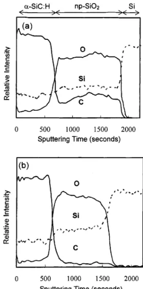
Figure 3 shows Auger depth profiles for
a-SiC:H/nanoporous silica film stacks prepared at two dif-ferent a-SiC:H deposition temperatures, 200 and 375 °C. The a-SiC:H film was deposited with a 3MS flow rate of 20 sccm at 1–10 mTorr for 10 s. The Auger depth profiles clearly show that carbon uniformly distributes in the nanopo-rous silica layer, and the carbon content in the nanoponanopo-rous silica film depends on the a-SiC:H deposition temperature. The uniform distribution of carbon indicates that the highly porous character of the nanoporous silica thin film allows a fast diffusion of carbon containing species in the nanoporous layer. The presence of oxygen in the a-SiC:H region is pos-sibly due to adventitious oxygen containing residual gas spe-cies in the HDP-CVD system, which was incorporated into the a-SiC:H film during the film growth. Table I lists Auger intensity ratios of carbon to silicon and carbon to oxygen in the nanoporous silica layer after the a-SiC:H deposition at
various substrate temperatures. The carbon/silicon ratio de-creases from 1.35 to 0.1 as the substrate temperature in-creases from 100 to 375 °C. It would seem rational to be-lieve that the presence of carbon in the nanoporous silica film is a consequence of direct interactions between the ac-tive plasma species and the silica film during the plasma FIG. 2. FTIR spectra of film stack A with various a-SiC:H deposition
tem-peratures:共a兲 100 °C, 共b兲 200 °C, 共c兲 300 °C, 共d兲 375 °C.
FIG. 3. AES depth profiles of film stack A. Before the deposition of the HDP-CVD a-SiC:H layer, the nanoporous silica thin film was annealed at 375 °C for 30 min in the HDP-CVD system. The deposition temperatures of the a-SiC:H film were:共a兲 200 °C and 共b兲 375 °C.
TABLEI. Auger intensity ratios of carbon to oxygen and to silicon for the nanoporous silica layer of film stack A for four different deposition tempera-tures of a-SiC:H. The C(KLL), O(KLL), and Si(KLL) Auger intensities were obtained from the same Auger depth profiles as the ones shown in Fig. 3.
Deposition temperatures of the a-SiC:H thin layer
(°C)
Auger intensity ratios
C/O C/Si
375 0.0435 0.10
300 0.1277 0.39
200 0.3684 0.76
deposition of the a-SiC:H overlayer. However, as will be shown later, residual hydrocarbon gases trapped in the HDP-CVD a-SiC:H film play a crucial role to introduce the car-bon containing species into the nanoporous silica film. The decrease of the carbon content in the nanoporous silica layer of the film stack with increasing a-SiC:H deposition tem-perature can be ascribed to the fact that the a-SiC:H film retains less hydrocarbons at higher deposition temperatures due to a denser microstructure. Consequently, the a-SiC:H film will supply less hydrocarbons to the underlying nanopo-rous silica layer.
Carbon diffusion into the nanoporous silica layer was also found to take place in film stack B, of which the a-SiC:H layer was first deposited on the Si substrate followed by spin-coating of the nanoporous silica thin film. The a-SiC:H film was deposited at 130 °C at a plasma power of 300 W, and the nanoporous silica film was then prepared in the clean room ambient and received the calcination treatment at 400 °C. Like film stack A, the AES depth profile of film stack B shown in Fig. 4 shows that carbon evenly distributes through the nanoporous silica layer. Since the nanoporous silica top layer has not been subjected to any plasma circum-stance, carbon diffusing into the nanoporous film is certainly not supplied by active plasma species. As will be discussed later, organic species in the sol-gel precursor were not an important contributor to the carbon content either. Therefore, the only source providing reactants to form carbon contain-ing groups in the silica film is from the underlycontain-ing HDP-CVD a-SiC:H layer, and gas transport in the film stack must occur during the high temperature calcination treatment of the nanoporous silica top layer.
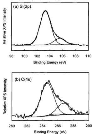
Figure 5 shows the C(1s) and Si(2 p) XPS spectra of film stack B. In the Si(2 p) spectrum, Si–O bonding in the silica matrix of the top nanoporous silica film gives the intense Si(2 p) peak at 103.3 eV. The shoulder peak around 105.5 eV is due to Pt(5s) electrons from the Pt island, which was deliberately sputtering-deposited on the sample surface for
charge correction. The Si(2 p) peak width is very close to the pristine nanoporous silica thin film and no noticeable signal at the low energy side was detected. When any one of the oxygen atoms bonded to a surface silicon atom of the silica matrix is replaced by any hydrocarbon species, the Si(2 p) peak should have a redshift from the silica peak. Table II lists the surface species most likely to be formed on the pore surface of the nanoporous silica layer after alkylation by the underlying a-SiC:H layer. Also listed in Table II are atomic partial charges on carbon and silicon atoms of the terminal groups. The atomic charges were calculated in terms of the modified Sanderson formalism, which is based on the prin-ciple of electronegativity equalization in a molecule.13–15To estimate the atomic charges on silicon and carbon atoms, we have to calculate the stability ratio共SR兲 of the two elements in the surface species. SR is an electronegativity equivalent and the calculation of the SR of an element in a molecule (SRM) is based on the concept that a molecule is a collection
of groups rather than a collection of atoms. The SR calcula-tion in the study was performed in a similar fashion to that proposed by Sastry.13 Since the terminal surface species are bonded to – O–SiO3w subgroups which constitute the
nan-oporous silica matrix, we need to estimate the geometric mean of the stability ratios of all the atoms in the – O–SiO3w subgroup (SRG) before we can calculate the
SRM’s for carbon and silicon atoms of the terminal surface
species. In the calculation, we assume that the charge distri-FIG. 4. AES depth profiles of film stack B. The a-SiC:H layer was deposited
on the Si wafer at 130 °C in the HDP-CVD system. The nanoporous silica thin film was then spin-coated on the a-SiC:H layer in the clean room ambient. The layer boundaries were marked with dash lines.
FIG. 5.共a兲 Si(2p) and 共b兲 C(1s) XPS spectra of film stack B, in which the a-SiC:H film was deposited between the nanoporous silica thin film and the silicon substrate. The peak in the Si(2 p) spctrum around 105.5 eV is due to Pt(5s) electrons emitting from the Pt island, which was deliberately sputtering-deposited on the sample surface for charge correction.
1070 Panet al.: Alkylation of nanoporous silica thin films 1070
bution in the – O–SiO3w subgroup on the film surface is not
much different from that inside the bulk, and, therefore, the SRG of the – O–SiO3w subgroup on the film surface is
comparable to that in the silica matrix. The SRG of a single
– O–SiO3w subgroup was first calculated in terms of
Sand-erson stability ratios of oxygen and silicon atoms, followed by the calculation of the group stability ratio of the – Si( – O–SiO3)3w subgroup and so on. The final average
SRGof the – O–SiO3w subgroup was obtained by iterative
calculation of the SRGof the – O–SiO3w subgroups until a
difference in the stability ratio between two successive cal-culations was smaller than one thousandth of the last one. The average SRG of the subgroup, – O–SiO3w, was thus estimated to be 4.59. From Table II, the atomic charge on silicon atoms of silica is estimated to be 0.391, and the six listed possible surface species can be divided into two groups in terms of the magnitude of the atomic charge on the Si atoms. Group A includes those silicon atoms bonded to oxy-gen containing groups, and group B includes those directly bonded to hydrogen or alkyl groups. Within each group, the difference in atomic charges on silicon atoms between dif-ferent chemical environments is too small to be of any sig-nificance for XPS curve fitting. For group A, the atomic charge on the Si atoms of the three terminal configurations is around 0.377. The small difference in the atomic partial charge between silica and the three surface configurations will not cause any noticeable change in the peak shape from the pristine silicon dioxide. On the other hand, Si atoms in group B have an atomic charge around 0.335. The difference of 0.06 in atomic partial charge between silica and group B may result in a Si(2 p) binding energy shift of 0.6 eV, assum-ing that the bindassum-ing energy shift is proportional to the atomic charge and the Si(2 p) electron energies for metallic silicon and silica are 99.6 and 103.3 eV, respectively. The curve
fitting using two synthesis Si(2 p) peaks, with one fixed for silica matrix, always merge the two synthesis peaks into one single peak. This might imply that the content of terminal alkyl groups bonded to silicon atoms is insignificant. A small redshift may not cause an apparent change in the peak profile in an XPS measurement without a monochromatic x-ray source. Moreover, since the surface layer is just a small por-tion of the probe depth of the XPS measurement, a weak Si(2 p) signal from the surface species may be dwarfed by the prevalent signal from the silica matrix.
For the C(1s) spectrum, the maximum intensity occurs around 284.9 eV, and the broad and asymmetric peak profile indicates the presence of multiple chemical states on the pore surface. As listed in Table II, six C(1s) chemical states are possible to exist in the nanoporous silica thin film after alky-lation. Based on the magnitude of the atomic charges, the six chemical states are divided into three groups. The result of the curve fitting for the broad C(1s) band using three syn-thesis Gaussian peaks is shown in Fig. 5共b兲. The peak at 284.6 eV can be assigned to the terminal carbon atom of alkyl groups higher than methyl group, such as ethyl or pro-pyl groups. The alkyl groups are either bonded to silicon or to oxygen atoms on the nanoporous silica surface, as sug-gested by group E in Table II. Because the intensity ratio of the C(1s) peak to Si(2 p) peak (⬃0.24) in Fig. 5 far exceeds the normally measured ratio (⬃0.05) for the as calcined na-noporous silica thin film without any modification, we be-lieve that the C(1s) signal is not due to residual organic chemicals in the sol-gel precursor, such as TEOS and tem-plate molecules, and hydrocarbon contamination during sample transfer is a trivial contributor to the C(1s) signal. This suggests that the detected C(1s) peak at 284.6 eV is a result of chemical interactions between hydrocarbons evolv-ing from the underlyevolv-ing a-SiC:H layer and the nanoporous silica film.
In Fig. 5共b兲, a shoulder peak on the high energy side can be easily observed, and the curve fitting resolved a peak at 286.5 eV. According to Table II, carbon atoms directly bonded to oxygen atoms on the silica surface 共group C兲 should have the highest C(1s) binding energy. Therefore, we tentatively assign the peak to carbons directly bonded to oxy-gen, i.e., the terminal group has an alkoxyl structure. In ad-dition to the two resolved peaks at 284.6 and 286.5 eV, one more C(1s) peak might exist in the C(1s) spectrum as sug-gested by Table II. In group D, the silicon atom is directly bonded by the terminal alkyl group, and, based on the calcu-lated atomic charge, the C(1s) electron energy of the carbon atom bonded to the silicon atom is estimated to be around 285.5 eV. When three component peaks, i.e., the three C(1s) groups in Table II, were used to synthesize the C(1s) spec-trum, the peak around 285.5 eV always has a much smaller peak area than the other two peaks as shown in Fig. 5共b兲. This suggests that hydrocarbons are more likely to react with oxygen atoms rather than silicon atoms on the pore surface in the nanoporous silica. On the other hand, the C(1s) peak at 284.6 eV, which is attributed to higher alkyl groups, has a much larger peak area than the C*– O–Si peak originated TABLEII. Possible terminal species on the pore surface of the nanoporous
silica layer after alkylation. The atomic charge on silicon and carbon atoms was calculated with the modified Sanderson formalism as described in Ref. 13. The listed binding energies for Si(2 p) and C(1s) electrons were esti-mated by assuming that the binding energy shift is proportional to the atomic charge. Terminal groups Atomic charges Binding energies Silicon Si(2 p) Silica O–SiO3 0.391 103.3 eV Group A C2H5O–SiO3 0.379 103.1 eV CH3O–SiO3 0.377 HO–SiO3 0.375 Group B C2H5– SiO3 0.336 102.7 eV CH3– SiO3 0.335 H–SiO3 0.331 Carbon C(1s) Group C CH3*CH2O–SiO3 0.002 286.5 eV *CH3O–SiO3 ⫺0.001 Group D CH3*CH2– SiO3 ⫺0.021 285.5 eV *CH3– SiO3 ⫺0.024 Group E *CH3CH2O–SiO3 ⫺0.033 284.6 eV *CH3CH2– SiO3 ⫺0.039
from group C, indicating that higher alkyl groups, such as the ethyl group, are the prevalent terminal groups on the pore surface. According to TDS study to be discussed later, a large quantity of ethane was desorbed from the a-SiC:H film at temperatures above 300 °C. For film stack B, the nanoporous silica film, which was spin-coated on the a-SiC:H deposited at 130 °C, has been calcined at 400 °C, and thus hydrocar-bon species diffusing from the underlying thin a-SiC:H layer may react with the nanoporous silica during the calcination treatment.
In our previous studies, hydrophobicity modification for nanoporous silica films was realized by trimethylsilylation in terms of hexamethyldisilazane 共HMDS兲 vapor treatment or trimethylchlorosilane 共TMCS兲 derivatization.5,6 Trimethylsi-lyl groups are found to be directly bonded to oxygen atoms on the pore surface after the film modification. In the present study, trimethylsilane was used as the plasma gas source for the a-SiC:H thin film deposition. It is very likely that 3MS gas molecules might be trapped in the HDP-CVD a-SiC:H layer. However, from the atomic charge calculation, we sug-gest that little trimethylsilyl group ( – Si(CH3)3) is present in
the nanoporous silica thin film. The calculated atomic charge on the silicon atom in the trimethylsilyl group is 0.231, which would correspond to a Si(2 p) binding energy shift from the silica matrix approximately by⫺1.67 eV. The large redshift should have given a distinct change in the XPS peak profile, but we did not observe any corresponding peak in the Si(2 p) spectrum shown in Fig. 5共a兲. Therefore, trimethylsi-lyl group is suggested not to exist in the nanoporous silica layer after alkylation.
Although active plasma species, such as methyl and trim-ethylsilyl radicals, may contribute to the carbon content in the nanoporous silica film in film stack A, carbon found in the spin-coated nanoporous layer of stack B, which received no plasma treatment, strongly suggests that alkane species desorbed from the a-SiC:H film are certainly a crucial sup-ply for the alkyl groups in the nanoporous silica layer. Friess-negg et al. have deposited a-SiC:H films by electron cyclo-tron resonance CVD 共ECR-CVD兲 and studied the influence of heat treatment on defect structure of the film.16 They found that a large amount of voids was created in the high density plasma a-SiC:H thin films and the interconnected open volumes can effectively trap gases from the ambient during the film growth or after deposition. The trapped gases are desorbed from the internal surfaces of these open vol-umes with increasing temperatures. They ascribed CHn
groups desorbed from the films at relatively low temperature (⬍400 °C) to hydrocarbons adsorbed on internal surfaces and trapped in voids. Figure 6 shows thermal desorption spectra of mass 16 (CH4) and mass 29 (C2H5) for
HDP-CVD a-SiC:H films deposited at different temperatures. It clearly shows that desorption of CH4 begins at temperatures
below 300 °C and prevails around 600 °C. Mass 29 has a similar desorption profile as methane at high temperatures, suggesting that ethane (C2H6) is probably an associative de-sorption product of methane. Because the preparation of the film stacks in the study did not exceed 400 °C, carbon found
in the nanoporous silica film must originate from these loosely bonded alkane species. It should be noted that the mass intensity of C2H5 ions is more than one order higher
than that of methane. This seems to agree with the previously discussed XPS result, which shows that most alkyl terminal groups in the nanoporous silica layer have an alkane struc-ture higher than methyl group. The nanoporous silica film is full of pores of ⬃4 nm in diameter,5,6 which can provide effective diffusion channels for small gas species evolving from the a-SiC:H underlayer during heat treatments. During thermal treatment, hydrocarbon molecules, such as methane and ethane, diffuse into the nanoporous silica network and react with hydroxyl groups and dangling bonds on the pore surface of the nanoporous silica layer. The alkylation leads to the formation of hydrophobic Si–O–CnH2n⫹1 groups in the
nanoporous silica film as shown by the XPS results. The CH4
and C2H5mass intensities in the TDS spectra of the a-SiC:H
film deposited at 375 °C are smaller than that deposited at 100 °C, suggesting that the low-temperature a-SiC:H film can accommodate more hydrocarbons. Accordingly, more hydrocarbons can evolve from the low-temperature a-SiC:H film and diffuse into the nanoporous silica film during ther-mal treatments. Moreover, as described earlier, a-SiC:H thin films deposited at higher temperatures are denser than those deposited at low temperatures. In other words, a-SiC:H films deposited at higher temperatures have a smaller open vol-ume. Figure 7 shows the plot of refractive indices and dielec-tric constants of the as-grown HDP-CVD a-SiC:H film as a function of the deposition temperature. The refractive index decreases with increasing the deposition temperature sug-FIG. 6. Thermal desorption spectra of共a兲 mass 16 and 共b兲 mass 29 for a-SiC:H thin films deposited at 100 and 375 °C.
1072 Panet al.: Alkylation of nanoporous silica thin films 1072
gesting that a denser a-SiC:H film was formed at higher temperatures. In particular, the increase in the refractive in-dex for the film deposited at 375 °C is much larger than those deposited at lower temperatures. This is in agreement with the FTIR results shown in Fig. 2, in which little Si–H absorbance was detected for the a-SiC:H film deposited at 375 °C, implying the formation of a denser film. As a result, the high temperature a-SiC:H film traps less gas molecules and gas transport in the amorphous film is somewhat re-strained in the dense film. This explains the AES results of film stack A, which shows that the carbon content in the underlying nanoporous silica film decreases with increasing the a-SiC:H deposition temperature.
Unlike film stack B, the nanoporous silica film in stack A was directly exposed to the plasma at the beginning of the a-SiC:H film deposition. Plasma dissociation of 3MS results in a great amount of hydrogen and active methyl containing species, such as trimethylsilyl radicals,17 and these active plasma species may directly react with hydroxyl groups and dangling bonds in the subsurface region of the nanoporous silica layer. Because of the ultrashallow probe depth of XPS measurements, we were not able to study the surface chemi-cal structure of the underlying nanoporous silica layer for film stack A. But we expect that, in the subsurface region of the nanoporous silica in film stack A, the chemical structure on the pore surface might differ somewhat from that in stack B, of which the nanoporous silica layer did not receive a direct plasma treatment. However, as the thickness of the a-SiC:H film gradually increased, it becomes more difficult for most active plasma species to penetrate through the growing a-SiC:H layer into the underlying nanoporous silica layer due to a relatively short lifetime of active radicals. Hence only trapped gas molecules, and possibly along with small hydrogen radicals from the plasma, can travel through the a-SiC:H film and the underlying nanoporous silica layer. The trapped gases may originate from radical and ion species recombined in the growing a-SiC:H film, as well as neutral molecules diffusing from the CVD system. According to pre-vious studies, hydroxyl groups in the nanoporous silica film decompose at temperatures above 350 °C, forming bridging oxygen or leaving dangling bonds.18,19In the present study, the underlying nanoporous silica film has been thermally
treated at 375 °C in the HDP-CVD system before the a-SiC:H deposition, thereby silanol group decomposition takes place during the thermal process leaving active sites on the pore surface of the nanoporous silica film. The active sites can then grasp the incoming gas molecules from the a-SiC:H film. We believe that, except in the subsurface re-gion, the chemical structure in the nanoporous silica layer of film stack A is likely to be similar to that of film stack B.
The presence of hydrophobic hydrocarbon groups on the pore surface can greatly enhance the resistance of the nan-oporous silica to moisture uptake, and hence improve the dielectric property of the film stack. Due to the large amount of hydroxyl groups and dangling bonds on the pore surface, the as-calcined nanoporous silica dielectric without any hy-drophobicity treatment usually has a very large leakage cur-rent and thus a rational dielectric constant cannot be mea-sured. In the present study, a very low effective dielectric constant of 1.65 can be obtained for the a-SiC:H/nanoporous film stack, and the dielectric property is rather stable in clean room ambient. Figure 8 shows that the dielectric constant gradually increases from 1.65 to 1.72 over 16 days. This study demonstrates that the HDP-CVD a-SiC:H deposition can greatly improve the dielectric property of the nanoporous silica dielectric layer. In addition, the a-SiC:H film can be used as the etch stop layer for the dual-damascene intercon-nect structure without seriously increasing the effective di-electric constant. The simultaneous implementation of hy-drophobicity modification for the nanoporous silica dielectric and the preparation of the etch stop layer in a single HDP-CVD system can greatly reduce the complexity of the inte-gration of nanoporous silica dielectrics into sub-100 nm in-terconnect technologies.
IV. CONCLUSION
We have successfully prepared film stacks of a-SiC:H and molecularly templated nanoporous silica thin films. The deposition of a-SiC:H thin films was carried out in an HDP-CVD system using 3MS as the precursor. Two film stack structures were studied: one is with the a-SiC:H layer on the nanoporous silica and the other with the nanoporous film on the a-SiC:H. According to Auger analyses, carbon contain-ing species uniformly distribute in the nanoporous silica thin FIG. 7. Refractive index and dielectric constant of the a-SiCx:H thin films
deposited at various substrate temperatures. F
IG. 8. Effective dielectric constant of film stack A as a function of the shelf time in clean room ambient.
film for both stack structures. The carbon introduced into the nanoporous silica thin film is believed to be due to alkylation on the pore surface by hydrocarbons trapped in microvoids in the a-SiC:H film, which are formed during the HDP-CVD deposition. The carbon content in the nanoporous film de-creases with increasing the a-SiC:H deposition temperature due to a denser a-SiC:H film formed at higher temperatures. We have studied the chemical structure of pore surfaces in the nanoporous silica layer of film stack B after alkylation by XPS. We used the modified Sanderson formalism to calculate atomic charges on silicon and carbon atoms in all possible terminal species on pore surfaces after alkylation, and thereby estimated the corresponding Si(2 p) and C(1s) elec-tron energies in the XPS spectra for these terminal species. According to the XPS analysis, terminal alkyl groups are mostly bonded to oxygen atoms on the pore surface of the nanoporous silica layer, i.e., the terminal surface species have the chemical structure of alkoxyl groups. The presence of hydrophobic hydrocarbon groups on the pore surface of the nanoporous layer can greatly enhance the resistance of the porous silica to moisture uptake, thereby improving the dielectric property of the film stack. An effective dielectric constant smaller than 1.7 can be obtained for the film stack. The a-SiC:H layer not only functions as a hydrophobicity modifier for the nanoporous silica film, but can also be used as an etch stop layer or barrier layer for the dual-damascene interconnect structure.
ACKNOWLEDGMENTS
This work was supported by the National Science Council of the Republic of China under Contract Nos.
NSC90-2722-2317-200 and NSC90-2215-E317-003. Technical support from the National Nano Device Laboratories is gratefully acknowledged.
1C. T. Kresge, M. E. Leonowicz, W. J. Roth, J. C. Vartuli, and J. S. Beck,
Nature共London兲 359, 710 共1992兲.
2
W. Zhou, J. M. Thomas, D. S. Shephard, B. F. G. Johnson, D. Ozkaya, T. Maschmeyer, R. G. Bell, and Q. F. Ge, Science 280, 705共1998兲.
3A. Stein, B. J. Melded, and R. C. Schroden, Adv. Mater.共Weinheim, Ger.兲
12, 1043共2001兲.
4C. W. Jones, K. Tsuji, and M. E. Davis, Nature共London兲 393, 52 共1998兲. 5
C. M. Yang, A. T. Cho, F. M. Pan, T. G. Tsai, and K. J. Chao, Adv. Mater. 共Weinheim, Ger.兲 13, 1099 共2001兲.
6A. T. Cho, T. G. Tsai, C. M. Yang, K. J. Chao, and F. M. Pan,
Electro-chem. Solid-State Lett., 4, G35共2001兲.
7
P. R. McCurdy, J. M. Truitt, and E. R. Fisher, J. Vac. Sci. Technol. A 17, 2475共1999兲.
8M. J. Loboda, Microelectron. Eng. 50, 15共2000兲.
9P. Xu, K. Huang, A. Patel, S. Rathi, B. Tang, J. Ferguson, J. Juang, C.
Ngai, and M. Loboda, IEEE Intercon. Technol. Conf. 1999, p. 109.
10
M. S. Lee and S. F. Bent, J. Phys. Chem. B 101, 9195共1997兲.
11M. S. Lee and S. F. Bent, J. Vac. Sci. Technol. A 16, 1658共1998兲. 12M. S. Lee and S. F. Bent, J. Appl. Phys. 87, 4600共2000兲. 13M. Sastry, J. Electron Spectrosc. Relat. Phenom. 85, 167共1997兲. 14
R. T. Sanderson, Chemical Bonds and Bond Energy 共Academic, New York, 1976兲.
15J. C. Carver, R. C. Gray, and D. M. Hercules, J. Am. Chem. Soc. 96, 6851
共1974兲.
16T. Friessnegg, M. Boudreau, P. Mascher, A. Knights, P. J. Simpson, and
W. Puff, J. Appl. Phys. 84, 786共1998兲.
17Q. S. Yu, C. E. Moffitt, D. M. Wieliczka, and H. Yasuda, J. Vac. Sci.
Technol. A 19, 2163共2001兲.
18F. M. Pan, A. C. Cho, C. M. Yang, K. J. Chao, T. G. Tsai, B. W. Wu, and
L. D. Chao, Electrochem. Soc., Proceedings of the First International Conference in Semiconductor Technology, 2001, p. 239.
19T. G. Tsai, A. T. Cho, C. M. Yang, F. M. Pan, and K. J. Chao, J.
Electro-chem. Soc. 149, F116共2002兲.
1074 Panet al.: Alkylation of nanoporous silica thin films 1074