國立高雄大學應用數學研究所
碩士論文
非拋物型能帶對量子校正的能量運輸模型中之能量鬆弛之
影響
Non-Parabolic Band Effects on Energy Relaxation for
the Quantum-Corrected Energy Transport Model
研究生:陳冠州撰
指導教授:劉晉良
Non-Parabolic Band Effects on Energy
Relaxation for the Quantum-Corrected
Energy Transport Model
by
Kuan-Chou Chen
Advisor
Jinn-Liang Liu
Department of Applied Mathematics,
National University of Kaohsiung
致 謝
記得兩年前的此時此刻,還在擔心是否能順利進入高雄大學研究所就讀,一 眨眼兩年很快就過去了,我即將從高大應用數學系碩士班畢業了。回想起這七百 多天在高大的種種,盡是充滿美好與難忘的回憶,我很慶幸能成為高大的一份 子。首先我要感謝的是我的指導教授 劉晉良老師,在研究所這兩年的細心指導 與支持,老師除了在學問上的指導使我獲益良多以外,其對學生教導的態度及追 求新知的熱忱更是令我留下深刻的好印象,在我論文每每遇到瓶頸而去請教老師 時,老師都會很不厭其煩的用最淺顯易懂的方式讓我去了解,這讓我在這段期間 學習到許多的知識,也讓我的論文能順利的完成,謹此致上我最誠摯的敬意和謝 意。 在這兩年期間,也承蒙系上每位老師以及系辦小姐的照顧,尤其是 郭岳承 老師在我們碩一修課的時間給我們在矩陣理論和矩陣計算的作業,讓我在線性代 數這方面的基礎更加穩固。另外也要感謝 陳仁純老師在我碩二寫論文的這段期 間對於程式方面的指導,老師很有耐心的回答我許多問題,讓我在數值部分能有 一些小小的結果。口試期間,也承蒙 郭岳承老師和 陳仁純老師費心審閱並提 供許多寶貴意見,使得本論文得以更加完備,學生特此謹致誠摯的謝意。 在這兩年求學過程中,也要感謝李俊德博士後學長,他計算出我們量子校正 的能量運輸模型中等比例縮放的部份,讓我們論文內相關的係數能更加方便的去 執行運用。另外,也要感謝我研究室的好夥伴,讓我在這些日子過的很快樂,跟 你們一起出遊、聚餐還有打球更是讓我開心且最難忘的寶貴回憶,希望大家畢業 後都能實現自己的理想,有著美好的未來。 最後,我要特別感謝我的家人給我的關心和祝福,你們不但給我良好的生活 環境,讓我無後顧之憂的繼續求學,也總是不辭辛勞的照顧我幫忙我以及支持 我,是我求學過程中繼續向前的原動力。再次感謝所有幫助過我及關心過我的 人,謝謝你們。Contents
1. Introduction . . . 1
2. The QCET Model . . . .4
3. Singularly Perturbed Formulation of QCET Model . . . . 11
4. Energy Relaxation with Non-Parabolic Band
Approxima-tion . . . 17
5. Numerical Results . . . 26
6. Conclusions . . . 27
非拋物型能帶對量子校正的能量運輸模型中之能量鬆弛之
影響
指導教授:劉晉良 教授 國立高雄大學應用數學所 學生:陳冠州 國立高雄大學應用數學所 摘要 量子校正的能量運輸模型是由描述穩定狀態中電子和電洞流的七條非線性對稱的 偏微分方程式所組成,它們的能量運輸,古典和量子位能是在一個等比縮放的奈米半導 體元件中產生。我們延伸量子校正的能量運輸模型中包含非拋物線型能帶結構之電子的 能量鬆弛項。我們得到詳盡的表示式有關於包含非拋物線型能帶影響的能量鬆弛項主要 依賴於電子的溫度。我們呈獻出非拋物線型的影響在熱電子之奈米元件中是非常重要 的。 關鍵字:量子校正、半導體、能量鬆弛、非拋物線型能帶結構Non-Parabolic Band Effects on Energy Relaxation for the
Quantum-Corrected Energy Transport Model
Advisor: Professor Jinn-Liang Liu Institute of Department of Applied Mathematics
National University of Kaohsiung
Student: Kuan-Chou Chen
Institute of Department of Applied Mathematics National University of Kaohsiung
ABSTRACT
The quantum-corrected energy transport (QCET) model consisting of seven self-adjoint nonlinear PDEs describes the steady state of electron and hole flows, their energy transport, and classical and quantum potentials within a nano-scale semiconductor device. We extend the energy relaxation term of QCET model to include the non-parabolic band structure for electron. We get explicit expressions of energy relaxation term involving the non-parabolic band effects and depending on the electron temperature. It shows that the non-parabolic effects are very significant for hot-electron nanodevices.
Keywords: quantum, semiconductor, energy relaxation, non-parabolic band structure.
1
Introduction
Semiconductor devices can be simulated by means of the semiconductor Boltzmann equation. However, this method is too costly and time consuming to model real problems in semiconductor applications. Acceptable accuracy can be reached by solving macroscopic semiconductor models which derived from the Boltzmann equation. The simplest models are drift-diffusion models which consist of the mass continuity equation for the charge carriers and a definition for the particle current density [14]. These models, however, are not accurate enough for submicron device modeling, owing to the rapidly changing fields and temperature effects [13].
The quantum-corrected energy transport (QCET) model consisting of seven self-adjoint nonlinear PDEs describes the steady state of electron and hole flows, their energy transport, and classical and quantum potentials within a nano-scale semiconductor device [7]. We extend the energy re-laxation term of QCET model to include the non-parabolic band structure for electron. Since the QCET equations are of parabolic type, the numeri-cal solution needs less effort than the hydrodynamic models. Moreover, the QCET equations can be written in a drift-diffusion formulation, therefore the numerical effort is comparable to the drift-diffusion models [13].
In this thesis, we compute explicitly about the energy relaxation term in terms of the temperature. For non-parabolic bands in the sense of Kane [13], the coefficients can be computed analytically. We use the Gamma function to
compute the energy relaxation term. And we present the energy relaxation term profiles for both parabolic and non-parabolic band structures.
We assume that the energy-band diagram of the semiconductor crystal is spherically symmetric and monotone in the modulus of the wave vector −→k, that non-degenerate Boltzmann statistics can be used and that a momentum relaxation time τ can be defined by τ (ε) ∼ ε−βN (ε)−1, where ε is the energy,
N (ε) denotes the density of states, and β > −2 is a parameter [13]. Then, using the general formulas for the coefficients and densities from [2], we get more explicit expressions than those of [2], involving the energy-band function ε(−→k ) and depending on the temperature.
Furthermore, we get analytical expressions under the additional assump-tion of non-parabolic bands in the sense of Kane [13]:
ε(1 + αε) = ~ 2 2m0 ¯ ¯ ¯−→k ¯ ¯ ¯2,
where ~ is the reduced Planck constant, m0 the effective electron mass, and
α > 0 the non-parabolicity parameter.
The numerical experiments are performed by employing the QCET model which is defined by different non-parabolic parameter α. The numerical re-sults in [13] show that the spurious velocity overshoot spike at the anode junction becomes smaller in the non-parabolic band case (α = 1/2), com-pared to the parabolic case (α = 0).
It is shown numerically that the energy relaxation is increasing nonlin-early for non-parabolic band structure with respect to the increment of the
temperature whereas it remains almost constantly for parabolic band struc-ture. This shows that the non-parabolic effects are very significant for hot-electron nanodevices.
2
The QCET Model
Based on the density gradient (DG) theory [1], the QCET model proposed in [7] is −∆φ = f1(φ) := q εs ⎡ ⎣ −nIexp( φ+φqn VT )u +nIexp(−φ−φVTqp)v + C ⎤ ⎦ = q εs (−n + p + C) , (2.1) −∆ζn = f2(ζn) := −ζn 2bn £ VT ln(ζ2n)− VT ln(nIu)− φ ¤ ,(2.2) −∆ζp = f3(ζp) := ζp 2bp £ −VT ln(ζ2p) + VT ln(nIv)− φ ¤ ,(2.3) −∇ · D4(φ)∇u = f4(u) : = q³neqpeq− n2Iexp( φqn−φqp VT )uv ´ τ ⎡ ⎣ nIexp( −φ−φqp VT )v + nIexp( φ+φqn VT )u +2√neqpeqexp(εkt−εi BTL) ⎤ ⎦ = q (neqpeq− np) τhn + p + 2√neqpeqexp(εkt−εi BTL) i, (2.4) −∇ · D5(φ)∇v = f5(v) :=−f4(u) , (2.5) −∇ · D6(ϕn)∇gn = f6(gn) := Jn·E + nWn, Wn :=− ωn− ω0 τnω , (2.6) −∇ · D7(ϕp)∇gp = f7(gp) := Jp·E + pWp, Wp :=− ωp− ω0 τpω , (2.7)
with the seven unknown functions φ, ζn = √n, (2.8) ζp = √p, (2.9) u = exp(−ϕn VT ), n = nIexp( φ + φqn VT )u, (2.10) v = exp(ϕp VT ), p = nIexp( −φ − φqp VT )v, (2.11) gn = Tnexp(− 5ϕn 4VT ), (2.12) gp = Tpexp( 5ϕp 4VT ), (2.13)
and the auxiliary relations
E = −∇φ (2.14) φqn = VT ln(ζ2n)− VT ln(unI)− φ, (2.15) φqp = −VT ln(ζ2p) + VT ln(vnI)− φ, (2.16) D4(φ) = qDnnIexp( φ + φqn VT ), (2.17) D5(φ) = −qDpnIexp(−φ − φ qp VT ), (2.18) D6(ϕn) = κnexp( 5ϕn 4VT ), (2.19) D7(ϕp) = κpexp(− 5ϕp 4VT ), (2.20) Jn = −qμnn∇(φ + φqn) + qDn∇n = D4(φ)∇u, (2.21) Jp = −qμpp∇(φ + φpn)− qDn∇p = D5(φ)∇v, (2.22) Gn = D6(ϕn)∇gn, (2.23) Gp = D7(ϕp)∇gp, (2.24)
where φ is the electrostatic potential, n and p the electron and hole densities, ϕnand ϕp the generalized quasi-Fermi potentials, Tn and Tp the electron and
hole temperatures, φqn and φqp the quantum potentials, E the electric field, Jn and Jp the electron and hole current densities, κn and κp the heat
con-ductivities, εs the permittivity constant of the semiconductor, C the doping
profile (impurity concentration), bn = h
2 12m∗ nq and bp = h2 12m∗ pq the material parameters measuring the strength of the gradient effects in the electron gas [1], τnω and τpω the carrier energy relaxation times, ωn and ωp the carrier
average energies, εt trap energy, εi intrinsic energy, and other symbols with
their values given in Table 1.
The system (2.1)-(2.7) models the steady state of electron and hole flows through the device by augmenting the macroscopic energy transport model (2.1), (2.4)-(2.6) [5] with the DG equations (2.2) and (2.3) [1]. The square roots of carrier densities in (2.8) and (2.9) were introduced in [18] as extra un-known functions to define the quantum (Bohm) potentials (2.15) and (2.16) by means of the generalized quasi-Fermi potentials ϕn and ϕp in (2.10) and
(2.11) [7, 18]. These quantum potentials represent the first order quantum corrections of the drift-diffusion fluxes as shown in (2.17) and (2.18). We observe from (2.2), (2.3), (2.15), and (2.16) that the QCET reduces to the classical ET model of [5] in the semiclassical limit h → 0. This model is also more general than the quantum drift diffusion models considered, for exam-ple, in [4, 10, 11, 12, 15, 16, 18] by including the energy transport equations (2.6) and (2.7) to deal with hotspot problems in nano-scale device design [17].
Note particularly that the right-hand side nonlinear functionals fi, i =
1,· · · 7, in (2.1)-(2.7) are all expressed in terms of their respective unknown variables φ, u, v, ζn, ζp, gn, and gp to illustrate that each functional can
be straightforwardly differentiated with respect to its variable and that each PDE is semilinear. All functionals are nonlinear due to the Slotboom-type transformations (2.10)-(2.13). Furthermore, these transformations also result in that all divergence operators in the left-hand sides of the system (2.1)-(2.7) are self-adjoint. This self-adjoint and semilinear formulation provides many appealing approximation features such as single finite element subspace for all seven variables, global and optimal convergence, and fast iterative solution [5, 8] with suitable conditioning scalings of the discrete system [6]. The Slotboom-type variables gn and gp in (2.12) and (2.13) were first introduced
in [5]. The relation between n and u in (2.10) implicitly defines the Slotboom variable u that generalizes the classical Slotboom variable to include the quantum potential. A similar generalization was also introduced in [16].
Let Ω ⊂ <2 denote the bounded domain of the silicon in Fig. 1. The
boundary ∂Ω = ∂ΩO∪∂ΩI∪∂ΩN is piecewise smooth with ∂ΩO= BC∪DE∪
AF denoting the Ohmic contacts, ∂ΩI = CD the silicon/oxide interface, and
∂ΩN = AB ∪ EF the Neumann boundary parts. The boundary conditions
φ = VO+ Vb on ∂ΩO, (2.25) ζ2n = 1 2 ∙ C + q C2+ 4n2 I ¸ on ∂ΩO, (2.26) ζp = nI/ζn on ∂ΩO, (2.27) ζp = ζn= 0 on ∂ΩI, (2.28) u = exp(−VO VT ) on ∂ΩO, (2.29) v = exp(VO VT ) on ∂ΩO, (2.30) gn = 300 exp(5VO 4VT) on ∂ΩO, (2.31) gp = 300 exp(−5VO 4VT) on ∂ΩO, (2.32) ∂φ ∂n = ∂u ∂n = ∂v ∂n = ∂ζn ∂n = ∂ζp ∂n = ∂gn ∂n = ∂gp ∂n = 0 on ∂ΩN, (2.33) ∂u ∂n = ∂v ∂n = ∂gn ∂n = ∂gp ∂n = 0 on ∂ΩI, (2.34)
where VO is the applied voltage, Vb is the built-in potential, and n is an
outward normal unit vector to ∂ΩN. The condition (2.28) on the interface is
Table 1. Physical constants
Symbol Physical meaning Value Unit
kB Boltzmann constant 1.38× 10⁻²³ J/K
q elementary charge 1.602× 10⁻¹⁹ C
m0 electron rest mass 9.11× 10⁻³¹ Kg
m∗n electron effective mass 0.98× m0 Kg
m∗
p hole effective mass 0.16× m0 Kg
ε0 permittivity of vacuum 8.85× 10⁻¹⁴ F/cm
εs silicon dielectric constant 11.7× ε0 F/cm
~ reduced Planck constant 1.054× 10⁻³⁴ J-s
VT thermal voltage 0.0259 V
nI intrinsic carrier concentration 1.5× 1010 cm−3
μn electron mobility 1350 cm2/V-s
μp hole mobility 480 cm2/V-s
Dn electron diffusion coefficient 34.659 cm2/s
Dp hole diffusion coefficient 12.432 cm2/s
TL lattice temperature 300 K
τ electron (hole) lifetime 10−8 s [2]
3
Singularly Perturbed Formulation of QCET
Model
Let l be the diameter (characteristic length) of the device. The standard singular perturbation parameter is the scaled Debye length λ defined as
λ2 = εsVT l2qC m (3.1) where Cm= max (x,y)∈Ω|C (x, y)| . (3.2) The magnitude of the doping remains roughly the same since the invention of transistor in 1947 [19] whereas the gate length of CMOS technology has been shrunk from 10000 nm (lC = 2.5· 10−5 m) in 1971 to 45 nm (lQ =
2.5· 45 · 10−9 m) in 2008. This means that the scaled Debye length which is
a crucial parameter in singular perturbation analysis has been enlarged from that of the classical device (with Cm = 1019 cm−3 = 1025 m−3)
λ2C = εsVT l2 CqCm = 11.7· 8.85 · 10 −12· 0.0259 (2.5· 10−5)2· 1.602 · 10−19· 1025 = 0.268· 10 −9 (3.3)
to that of the modern quantum device (with Cm = 1025 m−3)
λ2Q = εsVT l2 QqCm = l 2 C l2 Q ·λ2C = µ 2.5· 10−5 2.5· 45 · 10−9 ¶2 ·0.268·10−8 = 0.132·10−3. (3.4)
Apparently choosing the scaled Debye length as a singular perturbation parameter is no longer valid for nano-devices. However, singular effects are still present for such devices as shown by the numerical results below. The question is thus what kind of parameter is more feasible for nano-devices. Consider the following scaled intrinsic carrier concentration as a parameter
δ2 = nI Cm
. (3.5)
For both classical and quantum devices, we have
δ2Q = δ2C = 1.5· 10
10
· 106
1025 = 0.15· 10
−8 (3.6)
which is obviously more suitable for being a singular perturbation parameter. From the quantum potential equations (2.2) and (2.3), we have another parameter, namely, the scaled Planck constant defined by
2 = ⎧ ⎨ ⎩ 2bn VTl2 = ~2 6m∗nqVTl2 for electron, 2bp VTl2 = ~2 6m∗ pqVTl2 for hole. (3.7) Since the effective masses of the electron and hole are of the same order, the scaled Planck constant is denoted by this single symbol. It’s values for the classical and quantum devices are
2 C = 1.0542· 10−68 6· 0.98 · 9.11 · 10−31· 1.602 · 10−19· 0.0259 · 2.52· 10−10 = 0.8· 10−9 (3.8) 2 Q = l2 C l2 · 2 C = µ 2.5· 10−5 2.5· 45 · 10−9 ¶2 · 2C = 0.395· 10−4 (3.9)
The scaled Planck constant is moderately small indicating that for the 45nm device the quantum effect cannot be ignored any more.
We introduce the following scalings where the new dimensionless quanti-ties are marked with the subscript s
xs= x l, ys= y l, ∇s= µ ∂ ∂xs , ∂ ∂ys ¶ (3.10) ⎧ ⎪ ⎪ ⎪ ⎨ ⎪ ⎪ ⎪ ⎩ φs = Vφ T, ϕns = ϕn VT, ϕps = ϕp VT, φqns = φqn VT , φqps = φqp VT, Es =−∇sφs, ϕms = ϕm VT, ϕm = max(x, y)∈Ω © |ϕn| , ¯ ¯ϕp¯¯ª , (3.11) ⎧ ⎪ ⎪ ⎪ ⎪ ⎪ ⎪ ⎪ ⎪ ⎪ ⎪ ⎪ ⎪ ⎪ ⎪ ⎪ ⎪ ⎨ ⎪ ⎪ ⎪ ⎪ ⎪ ⎪ ⎪ ⎪ ⎪ ⎪ ⎪ ⎪ ⎪ ⎪ ⎪ ⎪ ⎩ ns = Cnm, ps = Cpm, ζns= ζn √ Cm, ζps = ζp √ Cm, nIs = CnmI = δ2, Cs = CCm, neqs = neq Cm, peqs = peq Cm, us= exp(−ϕu ms) = exp (−ϕns+ ϕms) , vs = exp(ϕv ms) = exp ¡ ϕps− ϕms ¢ , n = Cmδ2exp ¡ φs+ φqns− ϕms ¢ us, p = Cmδ2exp ¡ −φs− φqns+ ϕms ¢ vs φqns= ln(ζ2ns)− ln(δ2us)− φs, φpns =− ln(ζ 2 ps) + ln(δ 2v s)− φs, (3.12) ⎧ ⎪ ⎪ ⎪ ⎪ ⎪ ⎪ ⎪ ⎨ ⎪ ⎪ ⎪ ⎪ ⎪ ⎪ ⎪ ⎩ e D4(φs) = exp ¡ φs+ φqns− ϕms¢, e D5(φs) =− exp ¡ −φs− φqps+ ϕms ¢ , Jns= qDlJnnnI = eD4(φs)∇sus, Jps = qDlJp pnI = eD5(φs)∇svs, (3.13)
⎧ ⎪ ⎪ ⎪ ⎪ ⎪ ⎪ ⎪ ⎪ ⎪ ⎪ ⎪ ⎪ ⎪ ⎪ ⎪ ⎪ ⎪ ⎪ ⎪ ⎪ ⎨ ⎪ ⎪ ⎪ ⎪ ⎪ ⎪ ⎪ ⎪ ⎪ ⎪ ⎪ ⎪ ⎪ ⎪ ⎪ ⎪ ⎪ ⎪ ⎪ ⎪ ⎩ Tns= TTmn, Tps = TTmp, TLs= TTmL, Tm = max(x, y)∈Ω{Tn, Tp} , gns= T gn mexp(−5ϕm4 ) = Tnsexp ¡−5 4 (ϕns− ϕms) ¢ , gps = gp Tmexp(5ϕm4 ) = Tpsexp ¡5 4 ¡ ϕps− ϕms ¢¢ , e D6(ϕns) = exp ¡5 4(ϕns− ϕms) ¢ , e D7(ϕps) = exp ¡−5 4 ¡ ϕps− ϕms¢¢, Gns = κlGnTnm = eD6(ϕns)∇sgns, Gps = lGp κpTm = eD7(ϕps)∇sgps, Wns = l 2W n qDnVT, Wps = l2W p qDpVT. (3.14)
Then the potential equation (2.1) can be written as
−Vl2T∆sφs= qCm εs ⎡ ⎣ −δ 2 exp¡φs+ φqns− ϕms ¢ us+ δ2exp¡−φs− φqns+ ϕms¢vs+ Cs ⎤ ⎦
which can be rearranged in a simplified form as
−λ2∆sφs = f1(φs) := ⎡ ⎣ −δ 2exp¡φ s+ φqns− ϕms ¢ us+ δ2exp¡φs+ φqns− ϕms ¢ vs+ Cs ⎤ ⎦ . (3.15)
The DG equation (2.2) is transformed to −1 l2 p Cm∆sζns = − √ Cmζns 2bn £ VT ln ¡ Cmζ2ns ¢ − VT ln ¡ Cmδ2us ¢ − VTφs ¤ , = − √ CmζnsVT 2bn £ ln¡ζ2ns ¢ − ln¡δ2us ¢ − φs ¤ , which can be written as
− 2∆sζns= f2(ζns) :=−ζns £ ln¡ζ2ns ¢ − ln¡δ2us ¢ − φs ¤ . (3.16)
Similarly, Eq. (2.3) is scaled to − 2∆sζps = f3(ζps) := ζps £ − ln¡ζ2ps¢+ ln¡δ2vs ¢ − φs ¤ . (3.17) For the electron continuity equation (2.4), we have
−qDnCmδ 2 l2 ∇s· eD4(φs)∇sus = q ¡ C2 mneqspeqs− Cm2δ 4 exp¡φqns− φqps ¢ usvs ¢ τ Cm ⎡ ⎣ δ 2 exp¡−φs− φqps + ϕms ¢ vs
+δ2exp¡φs+ φqns− ϕms¢us+ 2√neqspeqsexp
³ εt−εi kBT ´ ⎤ ⎦ , or −δ2∇s· eD4(φs)∇sus = βnf4(us) : = βn ¡
neqspeqs− δ4exp
¡ φqns− φqps ¢ usvs ¢ ⎡ ⎣ δ 2 exp¡−φs− φqps+ ϕms ¢ vs+ δ2exp¡φs+ φqns− ϕms ¢
us+ 2√neqspeqsexp
³ εt−εi kBT ´ ⎤ ⎦ (3.18) where βn= l2 Dnτ.
Similarly, Eq. (2.5) is scaled to
−δ2∇s· eD5(φs)∇svs = βpf5(vs) := −βpf4(us) (3.19)
where βp = l
2
Dpτ.
For the ET equation (2.6), we obtain − ∇s· µ κnTm l2 De6(ϕns)∇sgns ¶ = qDnCmδ 2 VT l2 Jns· Es+ qDnVTCm l2 nsWns −∇s· ¡ ρ2n∇sgns ¢ = δ2Jns· Es+ nsWns, ρ2n = κnTmDe6(ϕns) qD V C . (3.20)
Similarly, we have for (2.7) −∇s· ¡ ρ2p∇sgps ¢ = δ2Jps· Es+ psWps, ρ2p = κpTmDe7(ϕps) qDpVTCm . (3.21) Dropping the subscript s in (3.15)-(3.21), the scaled QCET model is simplified to −λ2∆φ = f1(φ) = ⎡ ⎣ −δ 2exp¡φ + φ qn− ϕm ¢ u+ δ2exp¡φ + φqn− ϕm ¢ v + C ⎤ ⎦ , (3.22) − 2∆ζn = f2(ζn) =−ζn £ ln¡ζ2n ¢ − ln¡δ2u¢− φ¤, (3.23) − 2∆ζp = f3(ζp) = ζp £ − ln¡ζ2p¢+ ln¡δ2v¢− φ¤, (3.24) −∇ · (δ2n∇u) = f4(u) (3.25) = ¡ neqpeq− δ4exp ¡ φqn− φqp ¢ uv¢ ⎡ ⎣ δ 2exp¡ −φ − φqp+ ϕm ¢ v+ δ2exp¡φ + φqn− ϕm¢u + 2√neqpeqexp ³ εt−εi kBT ´ ⎤ ⎦ , −∇ · (δ2p∇v) = −f5(v) = f4(u) (3.26) −∇ · ¡ρ2n∇gn ¢ = f6(gn) = δ2Jn· E + nWn, (3.27) −∇ ·¡ρ2p∇gp ¢ = f7(gp) = δ2Jp· E + pWp, (3.28) with ⎧ ⎪ ⎪ ⎪ ⎪ ⎨ ⎪ ⎪ ⎪ ⎪ ⎩ λ2 = εsVT l2qC m, 2 = ~2 6m∗nqVTl2, δ 2 = nI Cm, δ2n = δ2De4(φ) βn , δ 2 p = −δ 2De 5(φ) βp , βn= l2 Dnτ, βp = l2 Dpτ, ρ2n= κnTmDe6(ϕn) qD V C , ρ 2 p = κpTmDe7(ϕp) qD V C . (3.29)
The boundary conditions (2.21)-(2.30) can be similarly scaled.
4
Energy Relaxation with Non-Parabolic Band
Approximation
We have to impose some physical assumptions on our model. The as-sumptions (H1)-(H2) below are imposed in order to get simpler expressions for the variables. The non-degeneracy assumption (H3) is valid for semicon-ductor devices with a doping concentration which is below 1019cm−3. Almost
all devices in practical applications satisfy this condition. The assumptions (H4) is the non-parabolic band structure in the sense of Kane [13] which is to abide by the law of conservation of momentum. All these assumptions follow from that of [13].
(H1) The energy-band diagram ε of the semiconductor crystal is spheri-cally symmetric and a strictly monotone function of the modulus k =
¯ ¯ ¯−→k ¯ ¯ ¯ of the wave vector k. Therefore, the Brillouin zone equals R3
and ε : R −→ R, k 7−→ ε(k).
τ (ε) = (φ0(2N0+ 1)εβN (ε))−1, β > −2, φ0 > 0, (4.1)
where N (ε) = 4πk2/
|ε0(k)| is the density of states of energy ε = ε(k) [2] and
N0 is the phonon occupation number [3].
(H3) The electron density n and the internal energy E are given by non-degenerate Boltzmann statistics.
(H4) Let the energy ε(k) satisfy
ε(1 + αε) = k
2
2m∗ (4.2)
The constant m∗is the effective electron mass given by m∗ = m
0kBT0/~2k02,
where m0is the unscaled effective mass, k0is a typical wave vector, and α > 0
is the non-parabolic parameter. Notice that we get a parabolic band diagram if α = 0.
The energy relaxation terms (2.6) and (2.7) can be written as the following general form [13]: W = T 2β−1 μ0τnw rβ(αT )( g1 pβ(αT, 2) − g2 pβ(αT, 3) ). (4.3)
Notice that the function rβ is in fact a polynomial:
rβ(αT ) = Γ(β + 2) + 5Γ(β + 3)αT + 8Γ(β + 4)(αT )2+ 4Γ(β + 5)(αT )3. (4.4)
Γ(s) = Z ∞
0
us−1e−udu, s > 0. (4.5)
The assumption (H4) implies γ(T u) = 2m∗T u(1 + αT u)[13]. Define the functions pβ(αT, l) = Z ∞ 0 1 + αT u (1 + 2αT u)2u l−β−1e−udu, (4.6) q(αT, l) = Z ∞ 0 (1 + αT u)12(1 + 2αT u)u 1 2+le−udu. (4.7) By letting αT u = x, we have 1 + αT u (1 + 2αT u)2 = 1 + x (1 + 2x)2 = (1 + x) 1 (1 + 2x)2 = (1 + x)(1− 4x + 12x2− 32x3+· · · ) = 1− 3x + 8x2− 20x3+· · · and hence pβ(αT, l) = Z ∞ 0 [1− 3αT u + 8(αT u)2− 20(αT u)3+· · · ]ul−β−1e−udu (4.8) Similarly, we have
(1 + αT u)12(1 + 2αT u) = (1 + x) 1 2(1 + 2x) = [1 + 1/2 1 x + 1/2· (−1/2) 1· 2 x 2+ 1/2· (−1/2) · (−3/2) 1· 2 · 3 x 3+ · · · ] (1 + 2x) = (1 + 1 2x− 1 8x 2 + 1 16x 3+ · · · )(1 + 2x) = 1 + 1 2x− 1 8x 2+ 1 16x 3 + 2x + x2 −14x3+1 8x 4+ · · · = 1 + 5 2x + 7 8x 2 − 163x3 +· · · and q(αT, l) = Z ∞ 0 (1 + αT u + 7 8(αT u) 2 − 3 16(αT u) 3+ · · · )u12+le−udu (4.9) The functions g1 and g2 in (4.3) can be computed in terms of n and T .
Under the assumptions (H1)-(H3), we can write g1(n, T ) = μ (1) β (T )T n, g2(n, T ) = μ (2) β (T )T 2 n (4.10)
with the temperature-dependent mobilities
μ(i)β (T ) = μ0
pβ(αT, i + 1)
q(αT, 0) T
−1/2−β, i = 1, 2. (4.11)
Here, the mobility constant μ0 is given by
μ0 = (3πφ0(2N0+ 1)m∗(2m∗)3/2)−1. (4.12)
Finally, we consider two cases of the parameters α and β, namely, (α = 0, β = 1/2) and (α = 1/2, β = 1/2). Note the momentum relaxation time
parameter β = 1/2 corresponding to the so-called Chen model which is shown in [13] to be more effective for handling the spurious velocity overshot peak than the so-called Lyumkis model with β = 0. Note also that, by (4.2), the case of α = 0 corresponds to the parabolic band structure whereas α = 1/2 corresponds to non-parabolic band structure.
Case 1. (α = 0, β = 1/2) Parabolic band. From (4.3), we have W1s = 1 μ0τnw r1/2(0)( g1 p1/2(0, 2) − g2 p1/2(0, 3) ) (4.13)
where s denotes after scaling, namely, the term in (3.27), and g1 = μ (1) 1/2(Ts)Tsns, g2 = μ(2)1/2(Ts)Ts2ns, μ(1)1/2(Ts) = μ0 p1/2(0, 2) q(0, 0) T −1 s , μ (2) 1/2(Ts) = μ0 p1/2(0, 3) q(0, 0) T −1 s , p1/2(0, 2) = q(0, 0) = Z ∞ 0 u1/2e−udu = √ π 2 , p1/2(0, 3) = r1/2(0) = Z ∞ 0 u3/2e−udu = 3 √ π 4 . Hence, we have g1 = μ (1) 1/2(Ts)Tsns = μ0Ts−1Tsns = μ0ns, g2 = μ (2) 1/2(Ts)T 2 sns = 3 2μ0T −1 s T 2 sns = 3 2μ0Tsns,
and W1s = 1 μ0τnw 3√π 4 ( μ0ns √ π/2 − 3/2μ0Tsns 3√π/4 ) = 3 2 ns τnw (TLs− Ts), (4.14) W1 = 3 2 n/Cm(TL/Tm− T/Tm) τnw , (4.15) where W1 is unscaled.
The energy-transport equation expressed in [13] is given by
−div J2s=−J1s· OsVs+ Wns. (4.16)
Now, we unscale it to obtain
−ldivJ2 l qμ0VT2Cm = −J1 l qμ0VTCm · l OV VT + 3 2 n/Cm(TL/Tm− T/Tm) τnw l2 μ0VT −divJ2 = −J1· OV + 3 2kB n(TL− T ) τnw −divJ2 = −J1· OV − 3 2kB n(T − TL) τnw , (4.17)
where VT = kBTm/q and J1 is the electron current density defined as that of
(2.21) in our model.
From (2.6) where the electron average energy is taken as ωn= 3/2kBTn,
nWn = −n ωn− ω0 τnw =−n3/2kBTn− 3/2kBTL τnw = −3 2kB n(Tn− TL) τnw (4.18) Which is exactly the same as (4.17) used in [13]. This verifies the two different scaling formulations between ours and that of [13] are indeed having the same relaxation term.
Case 2. (α = 1/2, β = 1/2) Non-parabolic band. Again from (4.3), we have
W2s = 1 μ0τnw r1/2( Ts 2 )( g1 p1/2(T2s, 2) − g2 p1/2(T2s, 3) ) (4.19) where g1 = μ (1) 1/2(Ts)Tsns, g2 = μ(2)1/2(Ts)Ts2ns, μ(1)1/2(Ts) = μ0 p1/2(T2s, 2) q(Ts 2 , 0) Ts−1, μ (2) 1/2(Ts) = μ0 p1/2(T2s, 3) q(Ts 2 , 0) Ts−1, p1/2( Ts 2, 2) = Z ∞ 0 1 +Ts 2 u (1 + Tsu)2 u1/2e−udu, p1/2( Ts 2, 3) = Z ∞ 0 1 +Ts 2 u (1 + Tsu)2 u3/2e−udu, q(Ts 2 , 0) = Z ∞ (1 + Ts 2 u) 1/2(1 + T
From (4.8) and (4.9), we have p1/2( Ts 2, 2) = Z ∞ 0 (1− 3 2Tsu + 2T 2 su 2 − 52Ts3u3+· · · )u1/2e−udu = Z ∞ 0 u12e−udu−3 2Ts Z ∞ 0 u32e−udu + 2T2 s Z ∞ 0 u52e−udu −52Ts3 Z ∞ 0 u72e−udu = Γ(3 2)− 3 2TsΓ( 5 2) + 2T 2 sΓ( 7 2)− 5 2T 3 sΓ( 9 2), p1/2( Ts 2, 3) = Z ∞ 0 (1− 3 2Tsu + 2T 2 su 2 − 52Ts3u3+· · · )u3/2e−udu = Z ∞ 0 u32e−udu−3 2Ts Z ∞ 0 u52e−udu + 2T2 s Z ∞ 0 u72e−udu −52Ts3 Z ∞ 0 u92e−udu = Γ(5 2)− 3 2TsΓ( 7 2) + 2T 2 sΓ( 9 2)− 5 2T 3 sΓ( 11 2 ), q(Ts 2, 0) = (1 + 1 2Tsu + 7 32T 2 su 2 − 3 128T 3 su 3+ · · · )u1/2e−udu = Z ∞ 0 u12e−udu +1 2Ts Z ∞ 0 u32e−udu + 7 32T 2 s Z ∞ 0 u52e−udu − 3 128T 3 s Z ∞ 0 u72e−udu = Γ(3 2) + 1 2TsΓ( 5 2) + 7 32T 2 sΓ( 7 2)− 3 128T 3 sΓ( 9 2), and hence
W2s = 1 μ0τnw r1/2( Ts 2 )( μ0ns p1/2(Ts2 ,2) q(Ts2 ,0) p1/2(T2s, 2) − μ0Tsns p1/2(Ts2 ,3) q(Ts2,0) p1/2(T2s, 3) ) = 1 μ0τnw r1/2( Ts 2 )( μ0ns q(Ts 2 , 0) − μ0Tsns q(Ts 2 , 0) ) = ns τnw r1/2( Ts 2)( TLs q(Ts 2 , 0) − Ts q(Ts 2 , 0) ), (4.20) W2 = n/Cm τnw r1/2( T /Tm 2 )( TL/Tm q(T /Tm 2 , 0) − T /Tm q(T /Tm 2 , 0) ), (4.21) where, by (4.4), r1/2( Ts 2 ) = Γ( 5 2) + 5 2TsΓ( 7 2) + 2T 2 sΓ( 9 2) + 1 2T 3 sΓ( 11 2 ). Since Γ(x + 1) = xΓ(x), for example, Γ(3 2) = √ π 2 , Γ(5 2) = 3 2 √ π 2 , Γ(7 2) = 5 2 3 2 √ π 2 , Γ(9 2) = 7 2 5 2 3 2 √ π 2 , we have the formula
Γ(k + 1 2) =
(2k)!√π
5
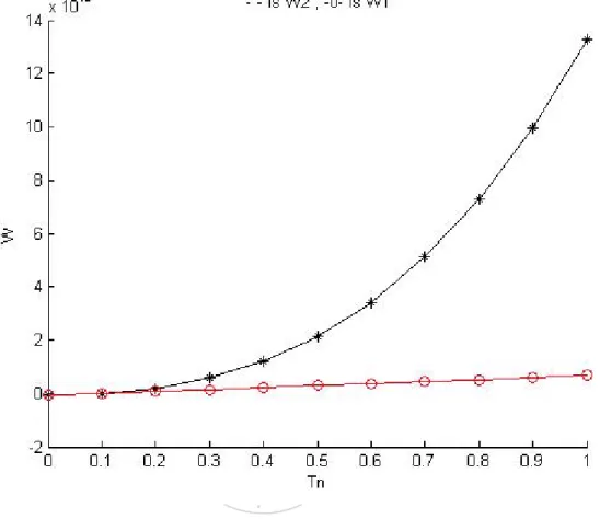
Numerical Results
The MOSFET device is shown in Fig. 1. In Fig. 2 the energy relaxation term for the two different values (0 or 1/2) of the non-parabolicity parameter α is shown, where the curves denoted by the circle and the star represent the relaxation term W1 (α = 0) and W2 (α = 1/2), respectively, vs the
different values of the electron temperature. Here, the maximal temperature values are Tm = 3423K, the lattice temperature values are TL= 300K. The
Cm is 5 · 1025m−3 and n is 1025m−3. The energy relaxation time τnw =
0.4 · 10−12s [7]. It can be seen that the maximal energy relaxation term
W2 = 1.3448· 1013m−3Ks−1 for the non-parabolic case is much larger than
W1 = 6.8475· 1011m−3Ks−1 for the parabolic case when Tn= 1. Fig. 2 thus
shows that the energy relaxation is increasing nonlinearly for non-parabolic band structure with respect to the increment of the temperature whereas it remains almost constantly for parabolic band structure. This shows that the non-parabolic effects are very significant for hot-electron nanodevices.
Fig. 2. Energy relaxation term W vs the electron temperature Tn.
6
Conclusions
In this thesis we have presented the QCET model and its scaled form. The energy relaxation term can be written analytically in terms of the electron density and the temperature for non-parabolic band structure in the sense
of Kane. There are two parameters, namely, the non-parabolicity parameter α and the momentum relaxation time parameter β. The variation of the en-ergy relaxation term is smaller in parabolic bands than that in non-parabolic bands. This shows that the QCET model describes the charge flow of elec-trons in a ballistic diode with reasonable accuracy. The spurious velocity overshoot spike at the anode juntion becomes smaller in the non-parabolic band case, compared to the parabolic case [13]. Therefore, we have shown that the non-parabolic effects are very important for hot-electron nanode-vices.
References
[1] M. G. Ancona, G. J. Iafrate, Quantum correction to the equation of state of an electron gas in a semiconductor, Phys. Rev. B 39 (1989) 9536-9540.
[2] N. Ben Abdallah and P. Degond, On a hierarchy of macroscopic models for semiconductors, J. Math. Phys. 37 (1996) 3306.
[3] N. Ben Abdallah, P. Degond, P. Markowich and C. Schmeiser, High field approximations of the spherical harmonics expansion model for semiconductors, Z. Angew. Math. Phys. 52 (2001), no 2, 201-230. [4] B. A. Biegel, M. G. Ancona, C. S. Rafferty, Z. Yu, Efficient
multi-dimensional simulation of quantum confinement effects in advanced MOS devices, NAS Tech. Report NAS-04-008, 2004.
[5] R.-C. Chen, J.-L. Liu, An iterative method for adaptive finite element so-lutions of an energy transport model of semiconductor devices, J. Com-put. Phys. 189 (2003) 579-606.
[6] R.-C. Chen, J.-L. Liu, Monotone iterative methods for the adaptive finite element solution of semiconductor equations, J. Comput. Applied Math. 159 (2003) 341-364.
[7] R.-C. Chen, J.-L. Liu, A quantum corrected energy transport model for nanoscale semiconductor devices, J. Comput. Phys. 204 (2005) 131-156. [8] R.-C. Chen, J.-L. Liu, An accelerated monotone iterative method for the quantum-corrected energy transport model, J. Comp. Phys. 227 (2008) 6266-6240.
[9] R.-C. Chen, J.-L. Liu, C.T. Lee, A singularly perturbed formulation of the quantum-corrected energy transport model, preprint, (2009). [10] D. Connelly, Z. Yu, D. Yergeau, Macroscopic simulation of quantum
mechanical effects in 2-D MOS devices via the density gradient method, IEEE Trans. Electron Devices 49 (2002) 619-626.
[11] C. de Falco, E. Gatti, A. L. Lacaita, R. Sacco, Quantum-corrected drift-diffusion models for transport in semiconductor devices, J. Comput. Phys. 204 (2005) 533-561.
[12] P. Degond, S. Gallego, F. Méhats, An entropic quantum drift-diffusion model for electron transport in resonant tunneling diodes, J. Comput. Phys. 221 (2007) 226-249.
[13] P. Degond, A. Jügel, P. Pietra, Numerical discretization of energy-transport models for semiconductors with non-parabolic band structure, SIAM on Scientific Computing 22 (2000) 986-1007.
[14] P. A. Markowich. The Stationary Semiconductor Device Equations. Springer, Wien, 1986.
[15] S. Odanaka, Multidimensional discretization of the stationary quantum drift-diffusion model for ultrasmall MOSFET structures, IEEE Trans. Comput.-Aided Design Integr. Circuits Syst. 23 (2004) 837—842.
[16] R. Pinnau, Uniform convergence of an exponentially fitted scheme for the quantum drift diffusion model, SIAM J. Numer. Anal. 42 (2004) 1648-1668.
[17] E. Pop, S. Sinha, K. E. Goodson, Heat generation and transport in nanometer-scale transistors, Proc. IEEE 94 (2006) 1587-1601.
[18] C. S. Rafferty, B. Biegel, Z. Yu, M. G. Ancona, J. Bude, R. W. Dutton, Multi-dimensional quantum effect simulation using a density-gradient model and script-level programming techniques, Proc. SISPAD (1998) 137-140.
[19] W. Shockley, Transistor Technology Evokes New Physics, Nobel lecture, December 11, (1956) 344-345.