384 IEEE ELECTRON DEVICE LETTERS, VOL. 31, NO. 5, MAY 2010
Operation of a Novel Device With
Suspended Nanowire Channels
Horng-Chih Lin, Senior Member, IEEE, Chia-Hao Kuo, Guan-Jang Li,
Chun-Jung Su, and Tiao-Yuan Huang, Fellow, IEEE
Abstract—We investigate the operation of a new device fea-turing a side-gate scheme and suspended poly-Si nanowire (NW) channels. The fabrication adopted a sidewall-spacer-etching tech-nique to form the poly-Si NW channels. The NW channels were further suspended using a simple wet-etching step. An interesting hysteresis phenomenon is observed in the I–V characteristics. In addition, a steep subthreshold swing (< 60 mV/dec) is also observed in the transfer curves. A scenario is proposed to explain the operation of such a device.
Index Terms—Hysteresis, MOSFET, nanowire (NW), poly-Si.
I. INTRODUCTION
I
N RECENT years, micrometer- and nanometer-size sus-pended structures formed with a micromachining process has received considerable attention owing to their great po-tential in electronics [1], [2] and biosensor applications [3], [4]. Relevant studies could be traced back a long time ago. For example, a device with a suspended gate structure was proposed more than 40 years ago [5]. In the device, the gate dielectric consists of an insulator and a sheet of air, and thus, the gate is movable during operation. Fabrication and analysis of these types of devices have received renewed interest [6]–[8]. One of the motives is their capability of breaking the physical limit of 60 mV/dec that is set for the subthreshold-swing (SS) of conventional MOSFETs under room-temperature op-eration [9]. Moreover, the devices exhibit interesting hysteresisI–V characteristics that are intriguing for memory and switch
applications [6], [7].
Typical planar process flow for device fabrication can be found in a previous work [6]. However, the gate-last process is non-self-aligned and unsuitable for device scaling. Moreover, the laterally etched structure is very deep, so a simple wet-etching process is not adequate to clear off the sacrificial layer, and dry chemical etching is indispensable. Although these
Manuscript received January 2, 2010; revised January 19, 2010. Date of publication March 22, 2010; date of current version April 23, 2010. This work was supported in part by the National Science Council of Taiwan under Contract NSC 96-2221-E-009-212-MY3. The review of this letter was arranged by Editor A. Ortiz-Conde.
H.-C. Lin is with the Department of Electronics Engineering and the Institute of Electronics, National Chiao Tung University, Hsinchu 300, Taiwan, and also with the National Nano Device Laboratories, Hsinchu 300, Taiwan (e-mail: [email protected]).
C.-H. Kuo, G.-J. Li, C.-J. Su, and T.-Y. Huang are with the Department of Electronics Engineering and the Institute of Electronics, National Chiao Tung University, Hsinchu 300, Taiwan (e-mail: [email protected]; [email protected]; [email protected]; [email protected]). Color versions of one or more of the figures in this letter are available online at http://ieeexplore.ieee.org.
Digital Object Identifier 10.1109/LED.2010.2041744
Fig. 1. (a) Stereo view of the proposed side-gated field-effect transistor with suspended poly-Si NW channels. The cross-sectional view along the middle of the device is shown in (b). Note that an air gap exists between the channel and the gate nitride.
concerns can be overcome by a judicious choice of top–down processes and employed materials, an alternative approach for resolving these issues is presented in this letter by resorting to a new device featuring suspended nanowire (NW) channels and side-gate configuration, as shown in Fig. 1.
II. DEVICESTRUCTURE ANDFABRICATION
The proposed device is evolved from a NW device developed previously [10], [11], which employs a sidewall-spacer-etching technique to form the NW channels. A brief process flow is shown with the major process steps in Fig. 2. First, an n+ poly-Si was deposited on a poly-Si wafer capped with thermal oxide, and then patterned to form the gate electrode [Fig. 2(a)]. Then, a Si3N4/SiO2 stack was deposited with low-pressure chemical vapor deposition (LPCVD). Afterward, a poly-Si layer was deposited also by LPCVD [Fig. 2(b)]. After the source/drain (S/D) implant [Fig. 2(b)], a photolithographic step was executed to generate the photoresist patterns covering the S/D regions. Subsequently, an anisotropic plasma etch step was performed to define the S/D regions. In this step, the sidewall NW channels were formed simultaneously in a self-aligned manner to the S/D [Fig. 2(c)] owing to the inherently larger vertical thickness of the poly-Si at the sidewall regions [10]. Note that to keep the NW channel undoped, the energy of the S/D implant was set at a low value. The S/D dopants were then activated with an annealing step. Next, for the suspended channel device, a wet-etching step using HF-based solution was applied to remove the sacrificial oxide layer between the NW channels and the silicon
LIN et al.: OPERATION OF A NOVEL DEVICE WITH SUSPENDED NANOWIRE CHANNELS 385
Fig. 2. Schematic diagrams of the major process steps for device fabrication.
Fig. 3. SEM image of a fabricated device taken after the sacrificial oxide etching.
nitride layer, thus forming the air gap [Fig. 2(d)]. Owing to the tiny dimensions of the NW channels, the etch depth is not deep, and thus, conventional wet etch using HF solution is feasible. The scanning electron microscopic (SEM) photograph of a de-vice taken after removing the sacrificial layer is shown in Fig. 3. Note that, in Figs. 1 and 2, the illustrated device contains two NW channels. We have also designed and fabricated devices with a single NW channel and found that their characteristics are basically the same as those with two NW channels.
III. RESULTS ANDDISCUSSION
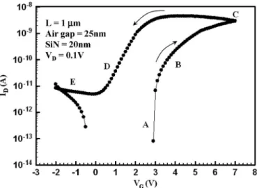
Fig. 4 shows typical transfer curves of a suspended-channel device with 20-nm-thick nitride and 25-nm-thick air gap. In the figure, the gate voltage (VG) was first swept forward from−2
to 7 V and then backward to−2 V. In forward sweeping, an SS as low as 53 mV/dec is achieved in the vicinity of VG= 3 V.
This value could be further reduced with a reduced sweeping voltage step [6]. Such an abrupt transition is an indication that the NW channels are attracted and moved toward the gate due to the electrostatic force exerted by increasing VG.
Fig. 4. Transfer characteristics of a device with air-gap and gate-nitride thicknesses of 25 and 20 nm, respectively. The arrows indicate the sweeping direction of the I–V curves.
Fig. 5. Illustrations of the pull-in mechanism of the suspended-channel device operated under forward sweeping.
In Fig. 4, it can be seen that a hysteresis window of 2.4 V is recorded at a drain current (ID) of 10−10 A. Again, this
is related to the motion of the suspended channels during forward- and reverse-sweeping measurements. Based on these observations, a scenario is proposed to explain the opera-tion mechanism of the device with the illustraopera-tions shown in Fig. 5(a)–(c), corresponding to specific operation conditions. In the beginning, the device is in theOFFstate with a low VG
386 IEEE ELECTRON DEVICE LETTERS, VOL. 31, NO. 5, MAY 2010
Fig. 6. Transfer characteristics of a device with air-gap and gate-nitride thicknesses of 35 and 11 nm, respectively. The arrows indicate the sweeping direction of the I–V curves. Owing to the larger air gap as compared with that of the device characterized in Fig. 4, the device exhibits a steeper SS.
(i.e., = 0 V), and the suspended channels and gate nitride are separated by the air gap [Fig. 5(a)]. As VG is swept forward,
the positive VGtends to induce electrons in the suspended NW
channels and leads to the attractive electric force between the channels and the gate. When such a force becomes sufficiently large with increasing VG, it could pull the channels to contact
the gate nitride [Fig. 5(b)]. This results in a sudden increase in
ID due to the significant reduction in effective gate dielectric
thickness, as indicated by point A in Fig. 4. However, the contact with the gate nitride occurs initially only at the central region of the NW channels, so the magnitude of ID increase
is limited. As VG increases further (region B in Fig. 4), the
portion of the NW channels that is in contact with the gate nitride increases gradually [Fig. 5(c)], further increasing ID.
In the beginning of reverse sweeping (region C in Fig. 4), the high attractive force would hold the NW channels, so most of the NW channels would remain in contact with the gate nitride for a while. In other words, a high IDis sustained until VGis
swept backward to the subthreshold region (region D in Fig. 4). In this region, a lowering in VGtends to repel the charges stored
in the channel, and thus, the attractive electric force between the channels and the gate nitride is reduced. In the meantime,
IDdecreases gradually as VGdecreases. Eventually, the device
turns off and releases the electrons residing in the channels (region E in Fig. 4). The NW channels would then be released from the nitride and returned to the suspended state [Fig. 5(a)]. We have checked and confirmed the good reproducibility of the I–V characteristics shown in Fig. 4 by repeating the mea-surements over ten times. We have also characterized another set of test devices having gate-nitride and air-gap thicknesses of 11 and 35 nm, respectively. Typical results are shown in Fig. 6. In this case, VG corresponding to the abrupt jump in
ID in forward sweeping (∼13.6 V) is larger than that shown
in Fig. 4, but an SS of 21.4 mV/dec is much steeper. These trends are obviously related to its larger air gap. We also found that the hysteresis disappeared in the succeeding measurements. Specifically, both forward and reverse sweeping curves for suc-ceeding measurements now coincide and trace essentially the same route as the backward curve during the first measurement, as shown in Fig. 6. This implies that the NW channels were stuck to the gate nitride after the first measurement. This could be ascribed to the large surface adhesion force that the elastic force of the NW channels cannot overcome in order to return to the suspended state. The origin of this phenomenon is still under investigation.
IV. CONCLUSION
In this letter, we have reported a new side-gated FET with suspended poly-Si NW channels. The fabrication is simple and low cost because no advanced lithography tools or processes are involved. The transfer characteristics of the fabricated de-vice exhibit a sub-60 mV/dec SS and a hysteresis behavior, which are attributed to the mobile action of the suspended NW channels.
REFERENCES
[1] B. Pruvost, H. Mizuta, and S. Oda, “3-dimensional design and analysis of functional NEMS-gate MOSFETs and SETs,” IEEE Trans. Nanotechnol., vol. 6, no. 2, pp. 218–224, Mar. 2007.
[2] W. C. Tang, T. C. H. Nguyen, and T. R. Howe, “Laterally driven polysil-icon resonant microstructures,” Sens. Actuators, vol. 20, no. 1/2, pp. 25– 32, Nov. 1989.
[3] F. Bendriaa, F. Le Bihan, A. C. Salaün, T. Mohammed-Brahim, and O. J. Bonnaud, “Study of mechanical stability of suspended bridge devices used as pH sensors,” J. Non-Cryst. Solids, vol. 352, no. 9–20, pp. 1246– 1249, Jun. 2006.
[4] A. Boisen and T. Thundat, “Design & fabrication of cantilever array biosensors,” Mater. Today, vol. 12, no. 9, pp. 32–38, Sep. 2009. [5] H. Nathanson, W. E. Newell, R. A. Wickstrom, and J. R. Davis, Jr., “The
resonant gate transistor,” IEEE Trans. Electron Devices, vol. ED-14, no. 3, pp. 117–133, Mar. 1967.
[6] N. Abelé, R. Fritschi, K. Boucart, F. Casset, P. Ancey, and A. M. Ionescu, “Suspended-gate MOSFET: Bringing new MEMS func-tionality into solid-state MOS transistor,” in IEDM Tech. Dig., 2005, pp. 1075–1077.
[7] N. Abelé, V. Pott, K. Boucart, F. Casset, K. Segueni, P. Ancey, and A. M. Ionescu, “Comparison of RSG-MOSFET and capacitive MEMS resonator detection,” Electron. Lett., vol. 41, no. 5, pp. 242–244, Mar. 2005.
[8] K. Akarvardar, C. Eggimann, D. Tsamados, Y. Singh Chauhan, G. C. Wan, A. M. Ionescu, R. T. Howe, and H.-S. P. Wong, “Analytical modeling of the suspended-gate FET and design insights for low-power logic,” IEEE
Trans. Electron Devices, vol. 55, no. 1, pp. 48–59, Jan. 2008.
[9] S. M. Sze and K. K. Ng, Physics of Semiconductor Devices, 3rd ed. New York: Wiley, 2006.
[10] H. C. Lin, M. H. Lee, C. J. Su, and S. W. Shen, “Fabrication and char-acterization of nanowire transistors with solid-phase crystallized poly-Si channels,” IEEE Trans. Electron Devices, vol. 53, no. 10, pp. 2471–2477, Oct. 2006.
[11] H. C. Lin and C. J. Su, “High-performance poly-Si nanowire NMOS transistors,” IEEE Trans. Nanotechnol., vol. 6, no. 2, pp. 206–212, Mar. 2007.