國
立
交
通
大
學
電機資訊學院 電子與光電學程
碩
士
論
文
主動矩陣式有機發光二極體驅動電路使用時間比例灰階
技術之研究
Time Ratio Grayscale Driving Circuits for Active Matrix Organic Light
Emitting Diodes
研 究 生:曾銘松
指導教授:黃 威 教授
主動矩陣式有機發光二極體驅動電路使用時間比例灰階
技術之研究
Time Ratio Grayscale Driving Circuits for Active Matrix Organic Light
Emitting Diodes
研 究 生:曾銘松 Student:Min-Sung Tseng
指導教授:黃 威 Advisor:Wei Huang
國 立 交 通 大 學
電機資訊學院 電子與光電學程
碩 士 論 文
A Thesis
Submitted to Degree Program of Electrical Engineering Computer Science
College of Electrical Engineering and Computer Science
National Chiao Tung University
in Partial Fulfillment of the Requirements
for the Degree of Master of Science
in
Electronics and Electro-Optical Engineering
August 2005
Hsinchu, Taiwan, Republic of China
中華民國九十四年八月
主 動 矩 陣 式 有 機 發 光 二 極 體 驅 動 電 路 使 用 時 間 比 例 灰 階 技 術 之 研 究
學生:曾銘松 指導教授
:黃 威
國立交通大學電機資訊學院 電子與光電學程﹙研究所﹚碩士班
摘
要
本論文提出一個改善發光效率之設計應用於主動有機發光二極體驅動電
路。而這個被驅動的畫素是以兩個電晶體及一個電容所組成的架構。藉由
增加發光時間及減少定址時間來提升傳統的時間比例灰階驅動方式之發光
效率。兩種可行方案被提出。取樣的移位暫存器採用倍速串列輸入將減少
定址時間。振輻調變編碼的使用將減少子圖框的數目進而增加發光時間。
結合上述兩種方案的驅動方式能夠提升 24%的發光。較高的發光特性,將
使得每個畫素面積減少,較小的畫素使得較高解析度的顯示器能夠被製
造。此外將驅動電路整合在面板上是最終目標,面板上常使用的多晶矽薄
膜電晶體有臨界電壓及遷移率變異的問題,而這些變異使得類比線路設計
不易實現於面板上。而這個改良的時間比例灰階驅動方式也是使用數位驅
動方式,在驅動電路部分它不需類比電路,他使得驅動電路完全整合於面
板上將成為可能。為了正確影像顯示,另外提出掃描訊號阻絕,以防止兩
個相鄰的掃描線切換時所造成的顯示資訊錯誤寫入。
這個主動矩陣式有機發光二極體驅動電路是用 0.6 微米 18V CMOS 製程
來模擬。由於點亮時間的限制,此一驅動電路適合應用於 QVGA 或低於此
解析度。
Time Ratio Grayscale Driving Circuits for Active Matrix Organic
Light Emitting Diodes
student:Min-Sung Tseng
Advisors:Dr. Wei Huang
Degree Program of Electrical Engineering Computer Science
National Chiao Tung University
ABSTRACT
Using improved luminance efficiency for the driving circuit of Active Matrix Organic Light Emitting Diodes (AMOLED) is presented in this thesis. The driven pixel is based on the structure with two transistors and one capacitor. We propose to enhance the luminance efficiency of conventional time ratio grayscale by increased lighting time and decreased addressing time. Two practical approaches to enhance luminance will be proposed. For decreased addressing time, shift register of sampling adopt double rate serial-in. For increased lighting time, amplitude modulation coding will reduce the number of sub-frame, and increase the lighting time. The combined method could enhance 24%. luminance. The higher luminance allows a small pixel. Small pixel will allow high resolution displays to be created. Moreover, the final goal is that driver circuits are integrated on the display panel. TFT by poly-silicon is always adopted. For poly-silicon thin film transistor (TFT), both mobility and threshold-voltage vary randomly across the plate. The former two variables would lead to analog circuit is hard to implement on panel. The improved time ratio grayscale also adopts the digital driving. There is no analog design in driver by this method. It is possible that the driving circuit is fully implemented to System on Panel (SOP). Another proposed scan signal gating for correct image display prevent from error-programming when adjacent scan line are toggling.
A prototype of this AMOLED driver is simulated by 0.6 um 18V CMOS technology. Because lighting time is limited, it is suitable for the Quarter Video Graphic Array (QVGA) or below the resolution.
Acknowledgements
The thesis is successfully. First, I would like to thank my advisor, Prof. Wei Hwang. He has given me a lot of guidance for three years, and his encouragement, concern, and instruction make me grow up greatly. It is also make me unforgettable. That is my honor that I could be the Prof. Wei Hwang‘s student.
I would also like to thank all of my laboratory friends. Among them are Wagon Chang, CS Hua, Lawrence Wu, Jerry Young and Chynny Chen, they give their enthusiasm to help me. By their assistance, my school life is more smoothly.
My colleagues, Howard Tsai, Heng Wang, Wisdom Shan, Anderson Tsai, Spring Ye, and Alex Hwang, have been a valuable source of moral support. I would like to thank all of them for their toleration during my years at NCTU.
My wife Te-Yin Liao, she is the most important source of inspiration and happiness when I am tired and depressed. I also appreciate my family, they have always been a tremendous source of encouragement and support.
CONTENTS
Chapter 1: Introduction ... 1
1.1 Keep Your Eye on The Future ... 1
1.2 History ... 2
1.3 Performance and Application ... 4
1.4 Scope of This Work... 6
Chapter 2: Related Techniques and Characterization for OLED ... 7
2.1 LED and OLED... 7
2.2 PLED and OLED ... 8
2.3 Light Emission Structure ... 9
2.4 Emission Properties ... 10
2.5 Color Present ... 10
2.5.1 Patterned Lateral RGB Emitters ... 11
2.5.2 Color Change Media ... 12
2.5.3 Color Filter ... 12
2.5.4 Color Stacked OLED ... 13
2.6 Electric Illumination Characterization ... 14
2.7 Matrix Addressing... 15
2.7.1 Passive Matrix ... 16
2.7.1.1 Pixel Structure ... 16
2.7.1.2 Pixel Addressing ... 16
2.7.1.3 Pixel Concern ... 17
2.7.2. Active Matrix Addressing ... 19
2.7.2.1 Pixel Structure ... 19
2.7.2.2 Pixel Addressing ... 20
2.7.2.3 Pixel Concern ... 21
2.7.2.3.1 Constant Current or Source Follower... 21
2.7.2.3.2 Driving Device Choice... 22
2.7.2.3.3 IR-Drop... 22
Chapter 3: AMOLED Review for Driving Design ... 25 3.1 Category... 25 3.2 Transistor Technologies ... 26 3.2.1 Poly Silicon ... 26 3.2.2 Amorphous Silicon ... 26 3.2.3 Organic Transistor ... 27 3.2.4 Crystalline Silicon ... 27 3.3 Analog Driving ... 28
3.3.1 Voltage Programming Pixel... 29
3.3.1.1 Voltage Programmed with 4T2C Pixel Structure ... 29
3.3.1.2 Voltage Programmed with 5T1C Pixel Structure ... 30
3.3.2 Current Programming Pixel ... 32
3.3.2.1 Current Programmed with Current-Copy Pixel ... 32
3.3.2.2 Current Programmed with Current-Mirror Pixel ... 33
3.4 Digital Driving... 34
3.4.1 Area Ratio Grayscale ... 34
3.4.2 Time Ratio Grayscale... 35
Chapter 4: AMOLED Driver Design ... 36
4.1 Active Matrix Driving... 26
4.2 Image Display... 40
4.3 Data Driver ... 42
4.3.1 Architecture ... 43
4.3.2 Serial to Parallel Circuit with Double Rate Serial-in ... 44
4.3.2.1 Image Mirror ... 46
4.3.3 Improved Time Ratio Grayscale with Amplitude Modulation... 47
4.3.4 Decoder and Analog Switch ... 50
4.3.5 Simulation Result and Summary ... 52
4.4 Scan Driver ... 55
4.4.1 Architecture ... 55
4.4.2 Sequential Scan with Image Handstand ... 56
4.4.2.1 Non-overlap with Scan Signal Gating ... 58
4.4.3 Cathode Electrical Switch for IR Drop Issue ... 60
4.5 Voltage Regulator... 63
4.5.1 Block Diagram of Voltage Regulator ... 65
4.5.2 Voltage Reference ... 66
4.5.2.1 Zero Temperature Coefficient ... 67
4.5.2.2 Architecture ... 70
4.5.2.3 Simulation Result and Summary ... 72
4.5.3 Pass Device Concern... 73
4.5.4 Frequency Response of Voltage Regulator ... 75
4.5.5 Voltage Regulator with OTA Structure... 77
4.5.6 Simulation Result and Summary ... 79
Chapter 5: Conclusions and Future Work... 81
5.1 Conclusions ... 81
5.2 Future Work... 82
TABLE CAPTIONS
Table 1-1 Every kind of compare of display characteristic---2
Table 2-1 Power dissipation in PMOLED displays with increasing size and resolution.---18 Table 3-1 Comparison of the saturation currents of a-Si:H and poly-Si TFTs---27
Table 4-1 Amplitude modulation coding---48 Table 4-2 Sub-frame value vs. physical output ---48 Table 4-3 Decoding relationship---51
FIGURE CAPTIONS
Fig. 1-1 FOLED by UDC---3 Fig. 1-2 Predict for OLED---5 Fig. 2-1 A typical LED---7
Fig. 2-2 A typical structure of an OLED device---9 Fig. 2-3 One pixel by lateral RGB Emitter---11 Fig. 2-4 One pixel by color change media---12 Fig. 2-5 One pixel by color filter---13
Fig. 2-6 Three pixels by color-stacked---13
Fig. 2-7 A typical brightness and voltage data relation for different color OLED---14 Fig. 2-8 A typical brightness and current data relation for different color OLED---15 Fig. 2-9 Structure of a simple matrix-type display---16
Fig. 2-10 Multiplexing principle for a matrix-type array of organic LEDs---17 Fig. 2-11 Principle of active matrix addressing of an OLED display---19 Fig. 2-12 Circuit diagram of an active matrix OLED---21
Fig. 2-13 Constant current pixel---22 Fig. 2-14 Source follower pixel---22 Fig. 2-15 IR-drop perspective---23
Fig. 2-16 A variant pixel with additional TFT---23 Fig. 2-17 Bottom and top emission structure---24
Fig. 3-1 Relation of operation frequency and field effect mobility for different technology--28 Fig. 3-2 Conventional voltage programming pixel with threshold compensation---29
Fig. 3-3 Timing diagram for 4T2C operation---30
Fig. 3-4 Novel voltage programming pixel with threshold compensation---31 Fig. 3-5 Timing diagram for 5T1C operation---31
Fig. 3-6 Current programmed with current-copy pixel---32 Fig. 3-7 Current programmed with current mirror pixel---33
Fig. 3-8 Sub-pixel arrangement in monochrome display using area-ratio technique---34 Fig. 3-9 A schema for time ratio gray-scale---35
Fig. 4-1 A schema for AMOLED driving---38 Fig. 4-2 Current source non-uniformity---38 Fig. 4-3 Scan lines timing diagram---39 Fig. 4-4 Image display---41
Fig. 4-7 Non-overlap clock generator---44
Fig. 4-8 Non-overlap clock for serial-in register---45 Fig. 4-9 Addressing time dissipation---45
Fig. 4-10 Image mirror with shift register control---46 Fig. 4-11 Save signal sequential for sampling latch---47 Fig. 4-12 Composition of each frame by proposition---50 Fig. 4-13 Output stage for data driver---51
Fig. 4-14 Output of data driver---52
Fig. 4-15 Lighting percentage in frame for convention driving---53 Fig. 4-16 Compared lighting percentage ---54
Fig. 4-17 Block diagram of scan driver---55
Fig. 4-18 Image handstand with shift register control---56 Fig. 4-19 Signal sequential for scan driver---57
Fig. 4-20 Adjacent scan line overlapping---58 Fig. 4-21Scan signal gating---59
Fig. 4-22 Cathode electrical switch---60 Fig. 4-23 I-R drop prevention---61 Fig. 4-24 Output of scan driver---62
Fig. 4-25 Voltage-current curve for poly-silicon pixel ---63 Fig. 4-26 Block diagram of linear regulators---65
Fig. 4-27 Linear regulator structures with PMOS---66 Fig. 4-28 Conceptual block diagram of bandgap---67 Fig. 4-29 Generation of PTAT voltage---68
Fig. 4-30 Bandgap structure---70
Fig. 4-31 Bandgap with start-up circuit---71
Fig. 4-32 Simulation for start-up circuit in bandgap---72 Fig. 4-33 Variation of the zero-TC---72
Fig. 4-34 Pass devices topologies---74
Fig. 4-35 Block diagram of linear regulator---76
Fig. 4-36 Frequency response of linear regulator under two different loads---77 Fig. 4-37 Linear regulator with OTA structure---78
Fig. 4-38 Simulated bode plot for loop response---79
Chapter1
Introduction
1.1
Keep Your Eye on The Future
Along with the technological advance, the mode of the person and the external world communication changes constantly. The daily life thing of today is through speech and graphics to take the data and communicate with the external world-- for example television, computer network, personal digital assistant, and the third generation cell phone system etc..
The display of the graphics and image depends on the display so that the display becomes the product that the modern people must get in touch with everyday. At the earlier period, the cathode ray tube is the representative of the display. However, the cathode ray tube has the huge problem in physical volume, his turns the disadvantage in the thin type and reducing weight. To get thin and flexible displays that roll up like paper, the researchers are already developing a number of innovative display approaches. These new displays include liquid crystal display, vacuum fluorescence display, organic light emitting display, plasma display etc..
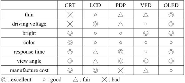
Although the current liquid crystal display occupies the market of the above even display in 80%, the color, visual angle, and thickness etc. still can't reach the perfect level. This makes other display techniques still contain existent space. Every kind of compare of display characteristic is on showing at table 1-1 [1-1]. In next generation, OLEDs will be a super star after LCDs. The most important difference between LCDs and OLEDs is that the OLEDs are emissive displays, which means that they generate their own light. LCDs are passive displays, and simply transmit or block an external light source to form an image. The light source for LCDs is typically either ambient light reflected by a metallic layer behind the display, or by a backlight system. Emissive displays don’t need ambient light to be viewable, and don’t require a backlight. This eliminates the cost, space, weight and power consumption of a backlighting system, and offers an image with much higher contrast. For example, OLED technology can be used to great benefit for both direct view and micro-display applications. In both cases, OLEDs offer higher efficiency and lower weight than competing liquid crystal displays, since they don’t require backlights or reflective light sources. These are very
displays offer a much wider viewing angle of 160 degrees. CRT LCD PDP VFD OLED thin ╳ ○ △ △ ◎ driving voltage ╳ ◎ △ ○ ◎ bright ◎ ○ ○ ◎ ◎ color ◎ ○ ○ ○ ○ response time ◎ △ ◎ ○ ◎ view angle ◎ △ ◎ ◎ ◎ manufacture cost ◎ ◎ ╳ △ ○
◎: excellent ○ : good : △ fair : ╳ bad
Table 1-1 Every kind of compare of display characteristic
Although large OLED panel prototypes have been shown at engineering shows, only a few products have shipped so far, and only in devices using much smaller displays, such as cell phones and car audio receiver. Nevertheless, OLEDs are attracting much attention [1-2][1-3] . There are some excellent characteristics in OLED such as fast response time, thin, high brightness, active emissive, wide viewing angle, wide operation temperature and flexible display. In this case, OLED have attracted great attention. Several famous companies are working on such next-generation displays, including Kodak which is the originator of the technology, IBM, Cambridge Display Technology, Philips, Pioneer and Sony.
1.2
History
In 1963, Pope et al. reported electroluminescence in single crystals of anthracene. Practical applications did not result from this early work because of the large driving voltages and the poor charge injection into the single crystals.
The problem of the large driving voltage was eliminated by the use of thin-film deposition techniques — Langmuir–Blodgett film deposition and vacuum sublimation of amorphous thin films of anthracene. The efficiency of these devices was still very poor before Tang and Van Slyke [1-4] could fabricate low-voltage (10 V), bright organic light-emitting devices from thin organic films of 8-hydroxyquinoline aluminum (Alq3).
This breakthrough was followed shortly afterward with the demonstration by Burroughes et al. [1-5] of electroluminescence in conjugated polymer films based on p-polyphenylenevinylene (PPV). At the same time, polymeric semiconductors that could be cast as thin films were developed. Scientists at the Xerox Research Center of Canada are developing semiconducting organic polymers that show promise for enabling the printing of electronic patterns on plastic substrates. Such materials could be alternatives to silicon transistors and lead to surprising applications, like a television screen rendered on a poster. Imagine monitors made of single sheets of flexible plastic.
In the last decade, we has seen a multidisciplinary thrust in designing stable high-performance organic and polymeric materials for flat panel display and plastic electronics applications and a concurrent effort in understanding the electronic and optical transport properties of such materials. The US Defense Advanced Research Project Agency (DARPA) is trying to speed development of FOLEDs (Flexible Organic Light Emitting Displays). In fact, a contract had been awarded to Universal Display Corporation to create flexible substrates that range from transparent plastic to opaque metal foils. One of several prototypes based on FOLED technology that is due to ship in two to three years is a flexible as shown in Fig. 1-1. FOLEDs sit on pliable surfaces such as thin plastic strips or metal foils, and can be laminated onto a wall, instrument panel, or piece of clothing, or bent or rolled, allowing retractable designs, like a window shade.
Transparent Organic Light Emitting Device (TOLED) is also developing, could be used as a display on windshields and cockpit windows. The combination of flexibility and transparency raises new possibilities for displays. Another prototype is a razor-thin Samsung cell phone that has a 2.2-inch display created with phosphorescent OLED (PHOLED) technology.
1.3
Performance and Application
OLED (Organic Light Emitting Display) panels use organic materials to produce light. When thin layers of this material are sandwiched between appropriate anode and cathode layers, a small voltage (typically 2 - 10 volts) applied across the material will cause it to emit light in a process called electroluminescence. This combination of anode materials, cathode materials and light emitting organic materials forms the OLED.
They can operate uniformly at very low levels as several nits (1 nit= cd/m2) for night time operation. They also operate well at very high brightness level as over 100,000 nits. However, OLEDs are usually specified to operate at more moderate level because operating lifetime is inversely proportional to brightness. At 100 nits, operating lifetimes of 5000-10000 hours are commonly reported [1-6][1-7][1-8]. Although the performance are adequate for some products, new materials are under development for increasing brightness and long lifetimes in more demanding applications.
In general, OLEDs are organized in a matrix structure of Rows and Columns with each pixel electrically connected between one Row lead and one Column lead. For applications that require low information content display the relatively simpler Passive Matrix (PM) addressing [1-9][1-10][1-11] scheme can be used. A passive matrix OLED (PMOLED) array consists of two sets of electrically isolated leads (Rows and Columns) arranged in orthogonal with an OLED at each intersection. An electronic switch is employed to address each of these rows.
Although the PMOLED panel structure has advantage of simplicity, the time available to drive each pixel decreases as the number of rows increases, driving up the peak brightness levels necessary to achieve adequate average brightness levels and causing the row line current to rise. Huge current cause large voltage drops in the row lines, and push the OLED operation to higher voltages where it is less power efficient. Since light emission from OLEDs
does not show any remanence, when an average each line has to excited with a peak luminance of N×Lm, N being the number of lines in the display. The light output from the OLED is proportional to the current that passes through it. Clearly, the currents required for higher resolutions, such as SXGA or UXGA, cannot be supported in passive matrix architecture without significant improvements in OLED efficiency. Due to all these limitations, Active Matrix (AM) addressing [1-12] [1-13] is necessary for high information content large area FPDs, and is the need to manage heat or power dissipation, display power efficiency is an important metric in portable system design.
Active matrix and passive matrix screens are two fundamental types of OLED display assembly. Each type lends itself to different applications. Driving the OLEDs with an active matrix leads to lower voltage operation, low peak pixel current, and a display with much greater efficiency and brightness. The role of the active matrix is to provide a constant current throughout the entire frame time, eliminating the high currents encountered in the passive matrix approach. iSuppli / Stanford Resources, an electronic-display-market research firm, sees a bright long-term future for the OLED approach and predicts the revenue generated globally by the technology will rise from $112 million in 2002 to $2.3 billion in 2008 , as shown in Fig. 1-2 shows. The predicts that OLED displays, particularly those using active-matrix technology, will become more popular during the next four years and generate an increasing amount of revenue.
1.4 Scope of This Work
Many famous companies have been actively developing OLED displays as a future display technology. Active matrix OLED technology opens up the route to high resolution and large color displays, which will be difficult to realize using passive matrix technology.
In this thesis, we propose to enhance the luminance efficiency of conventional time ratio grayscale by increased lighting time and decreased addressing time. Two practical approaches to enhance luminance will be proposed. For decreased addressing time, shift register of sampling adopt double rate serial-in. For increased lighting time, amplitude modulation coding will reduce the number of sub-frame, and increase the lighting time. The combined method is able to enhance the luminance. Besides, the main features of the AMOLED driver include selectable shift register for image mirror, selectable shift register for image handstand, scan signal gating for non-overlap scan, cathode electrical switch for I-R drop issue and voltage regulator which provide a lower voltage from a higher input voltage for different luminance and digital core .
In chapter 2, related technique and characterization for OLED are presented. In chapter 3, we take an AMOLED review for driving design. In chapter 4, design of AMOLED driver is described. Implementation details and the main simulation result are also given. Finally, conclusion and future work are given in chapter 5.
Chapter2
Related Techniques and Characterization for OLED
2.1 LED and OLED
Because they generate their own light, light-emitting diodes (LED) have long been considered the way to a better display. Conventional LED displays have been used successfully in giant screens usually seen in outdoor advertising, but these cannot be easily adapted to the small, high-resolution screens found in notebook computers. However, the OLED is an LED of a totally different kind - based on carbon-based molecules instead of inorganic semiconductors.
LED’s are special diodes that emit light when connected in a circuit. They are frequently used as “pilot” lights in electronic appliances to indicate whether the circuit is closed or not. A clear (or often colored) epoxy case enclosed the heart of an LED, the semi-conductor chip. The two wires extending below the LED epoxy enclosure, or the bulb indicate how the LED should be connected into a circuit. It is depend on each different material to send out the different wavelength light. Fig. 2-1 shows the typical LED. The product depends on the light wavelength and the factor that eye feel, can be divided into the infrared rays LED and the visible light LED. The material of the usage has decided the wavelength that the LED release light, and the material that suits to make the high brightness LED includes the AlGaAs, AlGaInP and the GaInN etc..
The organic light emitting diode calls Organic Electroluminescence (OEL) also. The principle of luminescence is alike to light emitting diode (LED), make use of the material characteristic equally. When electron and hole come close at emission layer, they capture one another and form a neutral, excited state. This form is called exciton. The exciton then decays and emits a photon. The OLED and LED are similar in many respect, but still have some different in basic structures. The most main discrepancy is the transmission of the charge. The OLED is not a mode that uses the band transmission, but it carry on the transmission of the charge by jump. This also make it the low rate of mobility, the impedance of OLED is higher than the impedance of LED. Besides organic light emitting diode can use various different base (substrates) materials in the low temperature (<150℃.) manufacturing. The defect of the organic light emitting diode lies in its life and operation temperature ranges.
2.2 PLED and OLED
According to the organic thin film material that OLED use, the organic light emitting diode can be divided to small molecule OLED and macromolecule OLED that is polymer-based. In the late 1970s, Eastman Kodak Company scientist Dr. Ching Tang discovered that sending an electrical current through a carbon compound caused these materials to glow. Dr. Tang and Steven Van Slyke continued research in this vein. In 1987, they reported OLED materials that became the foundation for OLED displays produced today. In 1990, Richard Friend at Cambridge University demonstrated the first polymer-based OLED using conjugated poly pr PPY.
In general, small-molecule devices are fabricated using vacuum deposition [2-1] and PLED are built using spin-coating or ink-jet printing [2-2][2-3]. In addition to in the material of differently, the small molecule OLED and PLED also is different in and component characteristics. Small molecule OLED outpace PLED with respect to efficiencies and lifetimes. Over 40 lm/W for sm-OLED by green phosphorescent and 20 lm/W for green PLED have been reported [2-4].
Over the past decade, great resources have been invested to develop better materials, new device structures, and processing technology for both systems. Today, it is still in technology development cycle, and both technologies hold great promise. In 1997, a glass-base 256x64 pixel display for an automotive radio consol was developed by Pioneer Electronic Corporation. Recently, Motorola introduced a cellular phone with eye-catching OLED display from Pioneer.
Many companies are focused on introducing monochrome, multi-color PMOLED display. Rapid progress is also being made to develop full-color AMOLED for higher-information display, e.g., internet-compatible cell phones, digital cameras and GPS.
2.3 Light Emission Structure
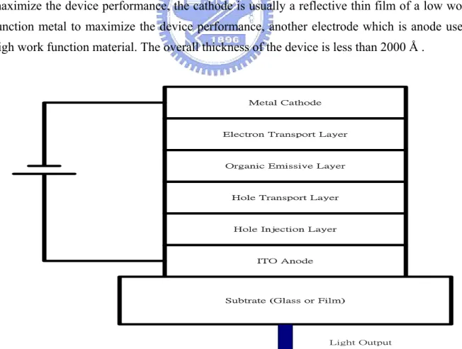
Fig. 2.2 shows the typical structure of an OLED device. OLED is a monolithic, thin film, semi-conductive device that emits light when voltage is applied to it. In its most basic form, an OLED consists of a series of organic thin films that are sandwiched between two thin-film conductors. On a glass substrate, the anode is an Indium Tin Oxide (ITO) layer, the hole-injection, hole-transport emissive and the electron transport layers are organic thin films which are optimized for each color. When voltage is applied, one layer becomes negatively charged relative to another transparent layer. As energy passes from the negatively charged (cathode) layer to the other (anode) layer, it stimulates organic material between the two, which emits light visible through an outermost layer of glass.
A wide variety of colors can be made by employing the specific organic materials. Doping or enhancing organic material helps control the brightness and color of light [2-5]. To maximize the device performance, the cathode is usually a reflective thin film of a low work function metal to maximize the device performance, another electrode which is anode use a high work function material. The overall thickness of the device is less than 2000 Å .
Metal Cathode Electron Transport Layer
Organic Emissive Layer Hole Transport Layer
Hole Injection Layer ITO Anode
Subtrate (Glass or Film)
2.4 Emission Properties
The structure of a conventional OLED is shown in Fig. 2-2. Electrons and holes are correspondingly injected from the cathode and anode, and migrate through the electron and hole transport layers. Electroluminescence is generated by radiative recombination of these carriers near the interface between the two transport layers.
The relation between the drive current density J and instantaneous luminance in the direction of substrate normal L(0) if an OLED is given by [2-4] [2-6]
J= η π V n C L C CE (0) ……… (2-1)
Where η is the quantum efficient. The constants Cn , CE and Cv depend on the refractive
index or the emission spectrum of the material. For an OLED using Alq3 as the emissive
material, Cn=1.1, Cv=427 lm/W, and CE=0.44V-1. Equation (2-1) gives the drive current
density required to achieve a given luminance. A luminance of 100cd/m2 is usually considered sufficient for video displays, corresponding to a drive current density of 3.6mA/cm2 for
η=1%.
2.5 Color Present
The color presents in OLED and can be divided into monochromatic, partial color and full color. Because the OLED has the characteristic of the self-moving optics and high brilliance, the display method of the monochromatic display and partial color still does not lack its usage situation. Current, green technology of organic light emitting diode in small molecule is the most mature, the blue and red optics have also started commercializing.
For high-information content display, the full color is an essential condition on the application of the display. Applications aiming at a full-color OLED display are making steady progress. Red, green and blue are necessary in each full color pixel. Up to present, several schemes exist for generating full color on the display of OLED. Prototypes have been demonstrated or reported by several research organizations, and each of them took a different approach to the fabrication. For example, the first approach employs patterned lateral RGB emitters, as shown in Fig. 2-3 [2-7]. This method has a good possibility of high luminous efficiency although patterning of organic layers is difficult. The second one utilizes blue OLEDs as a light source with fluorescent color arrays as color-changing media (CCM) to obtain RGB colors, as shown in Fig 2-4 [2-8]. This method does not require organic layer
patterning, but its low color change efficiency especially for red color is undesirable. The third approach uses white OLEDs with color filter array, as shown in Fig. 2-5 [2-9] [2-10]. This method has no need to pattern organic materials and is able to adopt the color filter technique used in LCD panel. But the efficiency of emitting light has a significant drop by passing through the color filters. Furthermore, there are other methods such as stacked RGB emitters. A stacked OLED was built at Princeton University with separate red, green and blue sub-pixels in a vertical, coaxial emitting geometry. Single pixels can be tunable to red, green, blue and white, as shown in Fig. 2-6 [2-11].
2.5.1 Patterned Lateral RGB Emitters
The simplest is to place red, green and blue(R, G and B) sub-pixels side by side and address them separately. Red, blue and green materials can be arranged in triads for each pixel through techniques such as precision shadow masking. This method blocks areas of the substrate surface for exact deposition and registration without gaps or overlap in color areas. Organic light emitting diode technology uses substances that emit red, green, blue or white light. Without any other source of illumination, OLED materials present bright, clear video and images that are easy to see at almost any angle.
To make use of the precise metal mask and CCD images position, red, green and blue by the order deposition constitute a pixel. Because the precise metal mask makes use of the super and thin lamella of metal, mask in the mechanical strength after taking shape will be under the influence of certain restrict, also cause an issue for position accuracy. OLEDs display development incline to the big size, over 10 inches, so will cause very big challenges, including the manufacture for the precise mask in big size and position technique.
Red OLED Green OLED Blue OLED
RED GREEN BLUE
2.5.2 Color Change Media
Single blue-emitting OLED may serve as a pump of R and G fluorescent color-changing media (CCM), which efficiently absorb blue light and reemit the energy as green or red light. This method does not require organic layer patterning. Its advantage is not to need the precise alignment to the technique, only needing the deposition for blue glow OLED component. A full-color organic display with 10 in. diagonal size was reported. This display was based on blue OLEDs with color-changing media. A potential problem to overcome in such displays is that “color bleeding” as light waveguided in the substrate can result in unintentional pumping of photoluminescence in adjacent pixels [2-6][2-12].
RED GREEN BLUE
Red CCM Green CCM Transparent Spacer
Blue OLED
Fig. 2-4 One pixel by color change media
2.5.3 Color Filter
The way is to use a single white-emitting organic LED and filter. The light pass through R, G, and B media or dielectric. Full-color effects also can be produced using a white emitting layer. A color filter array made through photolithographic techniques is inserted between the anode and substrate layers to produce red, blue and green effects. The combination of a white electroluminescent material and a color filter does not require precise alignment as rigorous as pixelized OLED displays. Nevertheless, the principal drawback of this approach is that much of the white OLED output must be removed by the filter to obtain the required primary colors. For example, up to 90% of the optical power from the white OLED is filtered in order to obtain a sufficiently saturated red pixel, with the result that the OLED must be driven up to ten times brighter than the required R-G-B pixel brightness.
RED GREEN BLUE Red Passband Filter Green Passband Filter Blue Passband Filter
White Light OLED
Fig. 2-5 One pixel by color filter
2.5.4 Color Stacked OLED
Current research on OLEDs is focusing on the integration of OLEDs into full-color, flat panel displays. The recent success in surface-emitting OLEDs has led to a new kind of integrated full-color pixel: the stacked OLED. In this technique, the layers that emit different colors are stacked on top of each other along with the required electrode to independently address each layer. The advantages of this approach in processing are that the patterning step and process control requirements are now essentially the same as for a monochrome display. Assuming that the patterning and addressing issue could be satisfactorily resolved, stacked OLEDs will triple resolution offered by the conventionally patterned RGB sub-pixels[2-12][2-13].
R-G-B
Color-Stacked OLED Color-Stacked OLED Color-Stacked OLED
2.6 Electric Illumination Characterization
Two drive methods are used in active-matrix OLED display: voltage driving and current driving. Voltage driving works by applying image signals to pixels as voltage data, which are converted to current data by pixel drive transistors. Converted current data flow to pixel OLED devices, which then emit light. Current driving works by applying image signals to pixels as current data, which are retained by pixel capacitors. Retained current data flows from pixel drive transistors to the OLED devices, which then emit light.
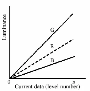
The voltage driving method applies voltage data to the source signal lines of the OLED display. Applied voltage data are converted to current data by pixel drive transistors and applied to OLED devices. Because current data converted by drive transistors have a nonlinear relationship to voltage data, the OLED device luminance has a nonlinear relationship to voltage data, as shown in Fig. 2-7. Current driving applies current data to the source signal line of the OLED display. Current data and OLED device luminance have a linear relationship, as shown in Fig. 2-8. Because OLED devices of RGB differ from on the current-luminance characteristics and the voltage-luminance characteristics, a adjustment circuit for brightness is necessary.
Fig. 2-8 A typical brightness and current data relation for different color OLED
2.7 Matrix Addressing
A display is an array of independently controllable pixels, the number of which depends on its dimension and resolution required by a particular application. Very large pixel counts are encountered in high-information content displays. For example, an NTSC standard TV screen requires 1.5x105 pixels. The addressing of a large number of pixels in an array is an important
issue in the display technology. Among the five addressing schemes used in electronic displays[2-14], direct addressing and matrix addressing are suitable for OLED-based systems. The direct addressing scheme, where each pixel is connected to an individual driver, can only be used for discrete indicators and simple alphanumeric displays with few characters. In this case, complex character patterns be realized using shadow masks. By comparison, inorganic LED alphanumeric displays are expensive to fabricate because of the many individual diodes required to make up a single character, each with its own contacts and leads. In a matrix addressed display, pixel are organized in rows (scan line) and columns (data line), and each pixel is electrically connected between one row lead, and one column lead. The addressing schemes where active electronic components are added to pixels are called active matrix (AM) addressing; while those without extra active components in the pixels are termed passive matrix (PM) addressing.
2.7.1 Passive matrix
2.7.1.1 Pixel Structure
As shown in Fig 2-9, passive matrix (PM) OLED displays stack layers in a linear pattern, much like a grid, with “columns” of organic and cathode materials superimposed on “rows” of anode material. Each intersection or pixel contains all three substances. External circuitry controls electrical current passing through the anode “rows” and cathode “columns,” stimulating the organic layer within each pixel. As pixels turn on and off in sequence, pictures form on the screen.
Fig. 2-9 Structure of a simple matrix-type display
2.7.1.2 Pixel Addressing
To address a matrix-type array of OLEDs is to perform a passive multiplexing. This mode of operation is well adapted since the electroluminescence phenomenon is fast (intrinsic response time in the 10-9 s range) and the current voltage characteristics of OLEDs are non-linear (diode-like). To achieve gray scales, the column drivers must be current sources since the pixel luminance is proportional to the drive current. There are two types of driving method [2-15] to implement gray scale . PAM (pulse amplitude modulation) and PWM (pulse width modulation) driving methods are well known. In increasing of the full color grayscale level and panel resolution, It is hard to exact current control. Therefore, the developed data driver IC is made by PWM method which has constant current source. The method of the
driving PM OLED is different from that of the LCD (liquid crystal display).
In this addressing mode, the matrix-type display is scanned line by line over the frame time. An electronic switch is employed to address each of the rows sequentially. When a line is selected, each pixel in the line is fed with a constant current pulse whole time duration is adapted to the desired level of brightness (pulse width modulation technique). Fig.2-10 schematically shows this principle of operation.
Fig. 2-10 Multiplexing principle for a matrix-type array of organic LEDs
2.7.1.3 Pixel Concern
To achieve an average display luminance of Ld , the pixel must be driven to an
instantaneous luminance of :[2-4] [2-6] L(0)= d r L M a d ……… (2-2)
where M is number of rows of a display, d is the duty cycle of a pulsed current addressing the pixels and ra is the aperture ratio of the display. The aperture ratio
a
r =WrWc/[(Wr+Dr)(Wc+Dc)] , where Wr, Wc are the row-line width and column-line width
respectively, and Dr, Dc are the gap width between the row lines and between the column lines in a PMOLED display respectively.
The instantaneous luminance requirement may limit the number of rows in a display. For a mean luminance 100 cd/m2, an instantaneous luminance up to 105cd/m2 limits the display row
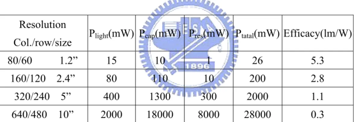
number to 500 for d = 50%, r = 100%. For a VGA display, this instantaneous luminance a translated to a peak current about 1A on the row lines. These huge currents cause large voltage drops in the row lines and push the OLED operation to higher voltage, and then lowers the power efficiency. Table 2-1 [2-16] shows the power dissipation increases dramatically in PMOLED displays with increasing size and resolution. This simulation shows that when increasing the display area by a factor of 4(2 times larger diagonal), the total power dissipation increases by a factor of 10. It seems a bigger passive matrix display becomes impractical, and it will be necessary to move to an active matrix technology. Therefore, PM OLED displays’ function and configuration are well-suited for text and icon displays in dashboard and audio equipment. Comparable to semiconductors in design, PM OLED displays are easily, cost-effectively manufactured with today’s production techniques.
Resolution
Col./row/size Plight(mW) Pcap(mW) Pres(mW) Ptatal(mW) Efficacy(lm/W)
80/60 1.2” 15 10 1 26 5.3
160/120 2.4” 80 110 10 200 2.8
320/240 5” 400 1300 300 2000 1.1
640/480 10” 2000 18000 8000 28000 0.3
Assumptions: 300um x 300um pixels, efficiency 15Cd/A (typical for green emitting OLEDs), average brightness over frame period 100 cd/m2 .
Light Production: Plight =IOLED x VOLED
Capacitive losses: Pcap = C x V2 x freq. Resistive losses: Pres = I2 x R
2.7.2 Active Matrix Addressing
2.7.2.1 Pixel Structure
Active matrix (AM) OLED displays stack cathode, organic, and anode layers on top of another layer – or substrate – that contains circuitry. The pixels are defined by the deposition of the organic material in a continuous, discrete “dot” pattern. Each pixel is activated directly: A corresponding circuit delivers voltage to the cathode and anode materials, stimulating the middle organic layer.
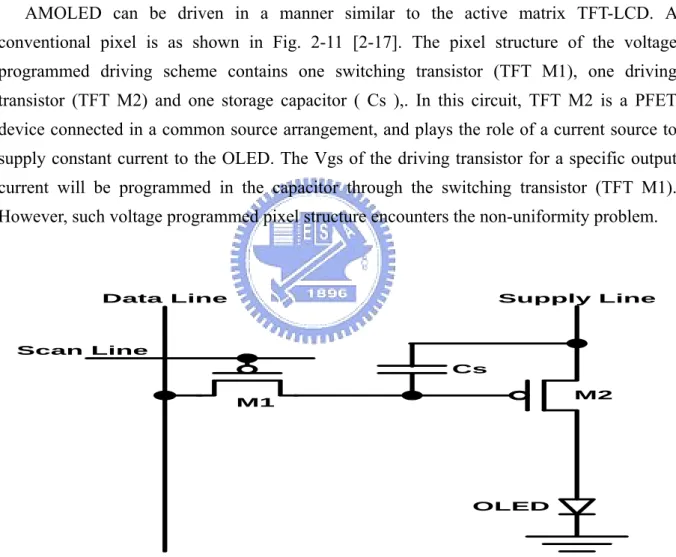
AMOLED can be driven in a manner similar to the active matrix TFT-LCD. A conventional pixel is as shown in Fig. 2-11 [2-17]. The pixel structure of the voltage programmed driving scheme contains one switching transistor (TFT M1), one driving transistor (TFT M2) and one storage capacitor ( Cs ),. In this circuit, TFT M2 is a PFET device connected in a common source arrangement, and plays the role of a current source to supply constant current to the OLED. The Vgs of the driving transistor for a specific output current will be programmed in the capacitor through the switching transistor (TFT M1). However, such voltage programmed pixel structure encounters the non-uniformity problem.
Scan Line
Data Line Supply Line
OLED
M2 Cs
M1
The saturation current of a TFT is usually approximated using the following equation(2-3), where W is the channel width, L is the channel length, Cox is the capacitance per unit area of the gate dielectric layer, Vth is the threshold voltage, and U is the field-effect mobility:
) (
2LUpCox Vgs Vth
W
Id = − 2……… (2-3)
From the asymptotic square equation for transistor current, it is obvious that the threshold voltage and mobility variation will result in great variation of the output driving current, and the non-uniformity in grey scales will be induced. Variations in threshold voltage and mobility depending upon implementation may add to luminance variations. With p-Si., initial variations are higher due to grain size and boundary variations[2-18]. With a-Si, time related electrical stress can give large threshold voltage variations[2-19] [2-20]. These luminance variations are tolerable if they occur gradually across a display, because the eye is insensitive to such variation. However, if they occur randomly from pixel to pixel, the eye can readily detect these variations.
2.7.2.2 Pixel Addressing
Fig. 2-12 show the active matrix addressed OLED(AMOLED). Each pixel in AMOLED has
a driving transistor in series with the OLED which supplies a constant current throughout the frame time. As shown in Fig. 2-11, the scan line of the display are sequentially scanned over the frame time. When a line is selected, all the M1 transistors in this line are switched-on and the voltage data are transferred on the gates of the M2 transistors. These data voltages are maintained on the gates of M2 transistors as M1 transistors are switched-off, when the next line is selected. A storage capacitor can be added to compensate the leakage current of M1 transistors. In this addressing mode, the current is supplied to the organic LED during the whole frame time. The necessary current levels are much smaller , but cause the setting times to be much longer. For a 300um x 100um pixel at typical luminance levels of 100 cd/m2, the transistor current is only a few micro-amps [2-21] [2-22] [2-23]. As for a typical pixel capacitance of 5 pF, it takes about 8us for a 3uA current to charge 5 pF though 5 volts.
AMOLED PIXEL AMOLED PIXEL AMOLED PIXEL AMOLED PIXEL AMOLED PIXEL AMOLED PIXEL
Column (Data) Driver
R o w ( S c a n ) D r i v e r AMOLED PIXEL AMOLED PIXEL AMOLED PIXEL
Fig. 2-12 Circuit diagram of an active matrix OLED
2.7.2.3 Pixel Concern
2.7.2.3.1 Constant Current or Source Follower
In order to continuously supply the current to the AMOLED pixel while the other scan lines are addressed. At least two TFTs are required for one pixel. The equivalent pixel circuit for this approach based on the n-channel TFT is shown in Fig. 2-13 and Fig. 2-14 [2-20]. Fig. 2-13 and 2-14 are the constant current arrangement the source follower arrangement, respectively. Due to the constant current circuit can eliminate the slight threshold voltage (Vth) shift of OLED and maintain the same output current level, it is preferred. That is the brightness remains even if a slight Vth shift of OLED is existent. Since OLEDs are extremely sensitive to moistures, wet process like photolithography is usually forbidden after the deposition of the organic layers. Therefore, the pixel circuits for AMOLED needs to be defined before the deposition of the organic layers. This limitation makes it very difficult to achieve the configuration as shown in Fig. 2-13, where the interconnection between the cathode of the OLED and the drain electrode of TFT M2 needs to be established. This implies that the constant current configuration for the n-channel TFT is difficult to realize for the two TFT circuit. For Source follower in Fig. 2-14, the drawback of this circuit is that the current depends upon the OLED voltage. The OLED voltage may vary from pixel to pixel and increase slowly with usage, ~0.1-1mV/hour, providing additional sources of non-uniformity.
Fig. 2-13 Constant current pixel Fig. 2-14 Source follower pixel
2.7.2.3.2 Driving Device Choice
To solve the above pixel issue, NFET in Fig. 2-14 is replaced by PFET. A current source with storage capacitor ( Cs ) is shown in Fig. 2-11. The OLED voltage dependence on current is eliminated with the circuit. The data voltage is written onto the data storage capacitor Cs when the TFT M1 gate line is brought to negative level. TFT M2 is a PFET device connected in a common source arrangement. TFT M2 play the role of a current source to supply constant current to the OLED. The current is proportional to (Vdd-Vdata-Vth)2 for Vth >Voled-Vdata
where Vth is the TFT threshold voltage.
2.7.2.3.3 IR-drop
OLED makes a direct current pass and emit light from the organic compound of the fluorescence excited by supplying electric field. The current is proportion to the data voltage which is written onto the data storage capacitor Cs. The period for the written data voltage is called addressing time. Since OLED is a current driver element, there is an IR drop issue on supply line along scan line direction while a turned on OLED is during addressing time, as shown in Fig. 2-15 [2-23]. A bad affect exist. That is, the pixel closed to supply line will be programmed an exact data voltage, but the far pixel will be programmed a wrong data voltage. The variation of gate-source leads to the divergent color. A variant of this circuit as shown in Fig. 2-16 uses an additional TFT to block any current flowing into the EL element while the scan line is addressed. The purpose is to reduce signal error due to resistance of the supply line.
Fig. 2-15 IR-drop perspective Fig. 2-16 A variant pixel with additional TFT
2.8 Top-Emission and Bottom-Emission
With the creation of a 13-in. color active-matrix organic electroluminescent (OEL) display, Sony (Tokyo, Japan) has demonstrated its proprietary top emission adaptive current (TAC) drive technology [2-24], which allows the fabrication of high-quality displays measuring over 10 in. The 800 x 600-pixel OEL display is presented as the largest of its type, presaging the use of OEL technology in a wider variety of applications beyond portable and compact devices.
Traditional polysilicon TFT drive systems often induce nonuniformity of luminance between the individual pixels, which makes it difficult to create a large-scale OLED display. TAC technology expands on the two-transistor driver circuit by using four transistors, of which two are paired to offset pixel variation for uniform luminance over the entire screen. A detail description for circuit is introduced in next chapter.
In addition, unlike the bottom-emission structure of traditional OLED displays where light is partly blocked by the TFT structure as shown in Fig. 2-17(a), the top-emission structure as shown in Fig. 2-17(b) emits light through the opposite side of the display matrix without any interference. In addition to increasing luminance, the pixels may be fabricated smaller to achieve higher resolutions.
(a) Bottom Emission Structure
(b) Top Emission Structure
Chapter3
AMOLED Review for Driving Design
3.1 Category
In AM addressing scheme, electronic switches are used with OLED for each pixel providing the means to retain the video information on a storage capacitor during the complete frame time. An additional active component, known as drive transistor is needed to provide the OLED with drive current at each pixel. The channel material of the TFTs can be Poly-silicon or amorphous-Silicon or even organic molecules. AM OLED pixels turn on and off more than three times faster than the speed of conventional motion picture film – making these displays ideal for fluid, full-motion video.
The AM addressing mechanisms are broadly categorized in two categories Analog
Digital
In the Digital driving methods [3-1] [3-2], the pixel circuit drives OLED in digital mode using constant current source i.e. OLED is either on or off. Grayscales are generated using either Area ratio grayscale (ARG) method or Time ratio grayscale (TRG) method or combination of both. In Area ratio grayscale (ARG) generation method, the pixel circuit is repeated for every bit required. In Time ratio grayscale (TRG) generation method, pulse width modulated current source is used. In the analog methods [3-1][3-2], each OLED is driven by controlled current source of varying current depending upon the brightness required. The controlled current source can be programmed by using either a current source or a data voltage source and should provide desired current throughout the frame time corresponding to the gray- level.
we will present the general concept of the AMOLED technique. Transistor technologies including a-Si:H, poly-Si, crystalline Si, and organics will be reviewed with respect to application to AMOLED displays. Then we will introduce some traditional pixel structures and driving schemes.
3.2 Transistor Technologies
polysilicon and amorphous silicon(a-Si) are known as semiconductors of TFTs used in active matrix organic light emitting diode panels. However, only expensive polysilicon backplanes were used for OLED production, because of their greater electron mobility. But researchers have started creating OLED structures on cheaper amorphous silicon substrates. In fact, IDTech—a joint venture between Chi Mei Optoelectronics and IBM—has demonstrated a 20-inch full-color OLED panel on an amorphous silicon substrate. In next, transistor technologies including a-Si:H, poly-Si, crystalline Si, and organics will be reviewed with respect to application to AMOLED displays.
3.2.1 Poly Silicon
Polysilicon is recently the active matrix technology of choice for direct view AMOLED displays. This is due to the high drive currents and the long term stability of the devices compared to amorphous silicon transistors. The field effect mobility is around 50~400 cm2/Vs and the on-off ratio is about 106 [3-3] [3-4]. It is suitable for pixel as well as driver integration on glass. Sanyo/Kodak demonstrated a stunning display at the SID’00 and Sony announced a new display at SID’01 Symposium. Thin film transistor technologies have large variations in output characteristics from device to device. These non-uniformities are due to the nature of the poly silicon material growth and the drift of the transistor characteristics during operation. These variations make it difficult to produce uniform current sources across many pixels. Since the pixel brightness is proportional to the current, any variation in the threshold voltage and mobility of the current drive transistor shows up as a variation in pixel brightness, creating a “salt and pepper” effect across the image. This effect is prevalent in poly silicon AMOLED displays. To avoid the objectionable effect, a lot of ideas are whether the driving method or the circuit attempts to correct for drive transistor variations.
3.2.2 Amorphous Silicon
Hydrogenated amorphous silicon (a-Si:H) TFT is of great interest because of the low cost and the large amorphous silicon manufacturing base[3-5]. Amorphous silicon deposition process tends to generate uniform initial threshold voltage, but the threshold voltage drift significantly over time. Besides, a-Si:H TFT has much smaller field mobility (<1cm2/Vsec) than poly-Si TFT (50~400 cm2/Vsec) [3-3] [3-6]. Therefore, the OLED driving current provided by an a-Si:H circuit will be much smaller than a polysilicon circuit. However, recent progress [3-3] [3-7] [3-8] in OLED efficiency make it possible to achieve a high brightness with much smaller current. For a typical OLED emission efficiency of 5.0 cd/A and a pixel
area of 2.0 x 10⁴ um2, a current of 4.0 x 10⁻⁷ A is need to achieved a pixel brightness of 100 cd/m2. Table 3-1 shows the comparison of the saturation currents of a-Si:H and poly-Si TFTs.
item
material a-Si:H TFT Poly-Si TFT
Typical Mobility(cm2/Vsec) 0.5 50
TFT W/L Ratio 10:01 10:01
Saturation Current(A) 2×10⁻⁶ 2×10⁻⁴
Table 3-1 Comparison of the saturation currents of a-Si:H and poly-Si TFTs
3.2.3 Organic Transistor
A new technology just starting to enter the display area is organic thin-film transistors (OTFTs). The technology [3-9] uses organic films to make up the active regions of the transistor. Displays and circuits can be made on flexible plastic substrates, because the entire fabrication process takes place at temperatures<100 . Using this process, analog and digital℃ circuits can be built on plastic substrate. Mobility on the order of 1 cm2/Vsec has been achieved with low threshold voltages, providing a performance level comparable to amorphous silicon transistors. It is hoped that greater stability will be achieved through refinements in materials and processes, making for a more robust approach.
3.2.4 Crystalline Silicon
Another approach to produce uniform OLED pixels is to implement the active matrix in a crystalline silicon technology where the transistor variations are small enough to produce uniform displays without correction. The process of silicon is limited to wafers, so techniques are suitable for microdisplay application. For example, eMagin is pursuing small area displays on silicon that can be used in head-mounted systems. Besides, due to the nature of higher mobility, crystalline silicon can operate at higher frequency. As shown in Fig. 3-1, it is very easy to integrated scan and data driver on a AMOLED chip if the crystalline silicon is used. Parallel driving method is also applied to compensate the lower mobility for amorphous silicon and polysilicon, but it will induce higher hardware cost.
Row(Scan Line) Driver
c-Si
Row (Scan line) Driver a-Si:H
c-Si
p-Si Column (Data Line) Driver
100M
10M
1M
100K
0.1 1 10 100 1000
Field Effecdt Mobility [cm^2/Vs]
F r e q u e n c y ( H z )
Fig. 3-1 Relation of operation frequency and field effect mobility for different technology
3.3 Analog Driving
Variations in threshold voltage and mobility depending upon implementation may add to luminance variations. Consequently, special pixel driver circuits are designed to overcome such difficulties in order to get thee good image quality. An important distinction between different pixel circuits is whether the data being written to the pixel is current or voltage. Voltage driving works by applying image signals to pixels as voltage data, which are converted to current data by pixel drive transistors. Converted current data flow to pixel OLED devices, which then emit light. Current driving works by applying image signals to pixels as current data, which are retained by pixel capacitors. Retained current data flows from pixel drive transistors to the OLED devices, which then emit light. In next, the different circuits and driving methods are reviewed.
3.3.1 Voltage Programming Pixel
3.3.1.1 Voltage Programmed with 4T2C Pixel Structure
The problem of variation of TFT threshold voltages was first tackled by Dawson et. al in 1998, using a four-TFT configuration [3-10][3-11]. An improved AMOLED pixel was designed which eliminates the effect of the transistor threshold voltage variation. The schematic for this pixel is shown in Fig. 3-2. The advantage of the four-transistor pixel is that it uses an auto-zero cycle to reference the data against the transistor threshold voltage eliminating the effects of the transistor threshold voltage variation.
Scan Line
Data Line Supply Line
OLED M2 C2 M4 M3 M1 C1 AZ(Auto Zero) Illuminate Line
Fig. 3-2 Conventional voltage programming pixel with threshold compensation
The functionality of TFT M1 through TFT M4 is identical to that in the current data pixel circuit . However, the driving method is more complex in that TFT M2’s threshold voltage must be established on the capacitors before writing data. With illuminate line low, the scan line is brought low with Vsup (Voltage on supply line) on the data line. Then, AZ is set low turning M3 on. A voltage across capacitor is developed that M2 forces to conduct. The illuminate line is brought high turning M4 off to isolate the circuit from the OLED. With M3 on, a voltage that is proportional to the threshold voltage of M2 is developed across both capacitors. The AZ input is brought high turning M3 off. The data voltage for luminance is the presented on the data lines. A portion of data voltage is coupled onto the capacitor C2 by capacitor C1. The scan line is brought high followed by a low on the SW input turning M4 on. The OLED current is, to a first
order, proportional to the square of the C2’s coupled data voltage. The step of the above operation is shown in Fig. 3.3.
Fig. 3-3 Timing diagram for 4T2C operation
3.3.1.2 Voltage Programmed with 5T1C Pixel Structure
Fig. 3-2 shows the conventional pixel structure and timing diagram of that structure which can compensate threshold voltage variation and the degradation of supply voltage. But is needs 3 control lines and complex driving signals for data line and control line. Moreover the data line must be alternated to supply voltage level with every row (scan) line time to store a threshold voltage.
A novel pixel structure having 5TFTs, 1 capacitor and 1 control line is shown in Fig. 3-4 [3-12] with a timing diagram for operation. M2, M3, M4 and M5 are switching TFTs, and M1 is driving TFT, which supplies constant current to OLED for a frame time. Vsus produces a constant voltage which is lower than the programmed data to sustain the gate node voltage of M1 for a frame time. The gate node voltage of M1, the right side of CST, increases to
‘VDD-VTH,M1’ by diode connected M1 and the left side of CST is set to programmed data
voltage during the current scan line time. After the row line time M4 and M5 are turned on and the potential of both side of CST decrease as a level of ‘VDATA-VSUS. From that time OLED
current flow by driving TFT M1, as follow equation (3-1).
Data Auto Zero Illuminate Scan Auto-Zero Phase Load Data Phase Illuminating Phase Vdata Vsup
) ( 2 GS,M1 TH,M1 OLED V V I = β − 2 [ { V -(V -V )}- V ] 2 − − TH,M1 DATA SUS TH,M1 = VDD VDD β 2 ( ) 2 VDATA−VSUS = β 2 ……… (3-1) Scan Line Data Line OLED M1 M4 M2 M3 CST M5 VSUS VDD
Fig. 3-4 Novel voltage programming pixel with threshold compensation
It has only one control line, scan line, for pixel operation and can use a whole row line time to program the data. The OLED current is controlled only by the VDATA and VSUS so that it has
good immunity against the degradation of panel supply voltage. The step of the operation is shown in Fig. 3-5.
Data Line
Scan Line
3.3.2 Current Programming Pixel
3.3.2.1 Current Programmed with Current-Copy Pixel
To avoid the non-uniformity problem induced by the variation of the threshold voltage and mobility of the TFTs, various pixel structures for current programmed driving scheme have been proposed[3-13] [3-14] [3-15]. Rather than the voltage signal to be programmed in the voltage programmed pixel structures, current signal on the data line is to be programmed into the pixel in these structures. In programming state, the scan line in Fig. 3-6 is activated, and the data line sinks for the specific TFT M2. This TFT is diode-connected by the supplementary switching TFT M3. Meanwhile, Vgs for the specific current through the TFT in saturation region is self-adjusted and stored in the storage capacitor (Cs). In the next state while the scan line is deactivated, often called the reproduction state, the configuration in the pixel is changed by the supplementary switching TFTs so that the stored Vgs on the driving TFT M2 will reproduce the current for the OLED. In this driving scheme, OLED current can be programmed and reproduced precisely, regardless the variation of the threshold voltage or mobility. Scan Data Line Vdd M2 Cs M3 M1 OLED M4
3.3.2.2 Current Programmed with Current Mirror Pixel
However, though the foregoing current programmed pixel structures seem immune to the process variation at first glance, it takes a vary long time to charge the data line in the programming state due to the current needed is vary small (nA~uA). Even though the current programming method can be applied to achieve excellent image quality, its panel driving speed is too slow to implement high resolution displays.
Other current programmed circuits have been proposed, Fig. 3-7 show the scheme [3-16] proposed by Sony Corporation. To set the OLED current, the scan line input is brought low while pulling or sinking the data current out of the data line. TFT M1 and TFT M2 are turned on by the scan line. TFT M1 operates as a data switch allowing current to flow from the pixel circuit into the data line. TFT M2 functions as a switch changing operation of TFT M3 to that of a diode, which allows adjustment of the capacitor voltage for matching TFT M3’s drain to source current to Idata. M4 drives the OLED based upon the capacitor voltage. The width of
TFT M3 is large than the width of TFT M4. By this way, we can adjust the aspect ratio of the TFT M3, M4 to achieve the current mirror ratio needed. Thus, a larger current will change the data line during the programming state, and the current driving OLED is still small. This allows the data current to be larger in order to set the pixel current within a scan time for low luminance levels.
3.4 Digital Driving
A full color display is more and more important in a life application. There are two types of driving method for Fig. 2-11. The analog driving and digital driving methods are well known. For analog driving, the intensity of each color is controlled by varying the amplitude of voltage applied to the sub-pixel during a picture frame.
The tendency, seems to be in favor of digital driving. For instance, Seiko-Epson use what they call area ration grey scale (ARG) in conjunction with time ration gray scale (TRG) [3-1][3-2].In digital driving, each EL element is connected to a switch. The stored voltage range must exceed the worst-case threshold voltage to operate correctly. By pushing the driving transistor into its linear operating region, the pixel circuit operates in a digital mode, being fully on or off. The method can reduce the threshold voltage sensitivity of display image.
3.4.1 Area Ratio Grayscale
Fig. 3-8 show the ARG method, the number of grayscales is proportional to the total number of sub-pixels of equal size to connect to the supplied voltage. In this driving scheme, the idea is to divide an elementary pixel in sub-pixel and to have driving TFT in each sub-pixel working either in the ‘on’ or the ‘off’ state. In other words, no intermediate voltage values are used on the gate of the driving TFTs. For example, if the elementary pixel is divided into two sub-pixels, four grey levels (22) can be obtained. However, to use this gray-scale control method is not expected to attain high resolution, since the decrease of a pixel pitch may be difficult. In addition, it is hard to fabricate the TFT-OLEDs with large gray scale level because further increase of the number of sub-pixels may be difficult.
3.4.2 Time Ratio Grayscale
This is implemented by dividing each picture frame into sub-frames with serial scan. During a sub-frame, all pixels are addressed – lit pixels are addressed by a specific voltage and then the display voltage is applied to the entire screen lighting those during the lighting time. As Fig. 3-9 [3-17][3-18], each sub-frame has a weighting ranging from 1 time unit to 32 time units for a typical six sub-frame arrangement. Time Unit depends on size and the number of pixels on the screen. This is a purely digital time-ration control mechanism, which is a key advantage as it eliminates any unnecessary digital to analog conversions, making the OLED technology ideal for the all-digital age. The OLED is lighting for different amounts of time to obtain different brightness level, and then obtain the different gray scales.