國 立 交 通 大 學
電子工程學系電子研究所
碩 士 論 文
二氧化矽薄膜所誘發之選擇性混合效應
對砷化銦鎵量子井之影響
Studies of SiO
2-Induced Selective Disordering
of InGaAs/GaAs Quantum Wells
研 究 生: 陳 雅 婷
指導教授: 李 建 平 博士
二氧化矽薄膜所誘發之選擇性混合效應對砷化銦鎵量子井之影響
Studies of SiO
2-Induced Selective Disordering of InGaAs/GaAs Quantum Wells
研 究 生:陳雅婷
Student:Ya-Ting Chen
指導教授:李建平 博士
Adviser:Dr. Chien-Ping Lee
國 立 交 通 大 學
電子工程學系 電子研究所
碩 士 論 文
A Thesis
Submitted to Department of Electronics Engineering
Institute of Electronics
College of Electrical and Computer Engineering
National Chiao Tung University
in Partial Fulfillment of the Requirements
for the degree of
Master
in
Electronics Engineering
June 2010
Hsinchu, Taiwan, Republic of China
i
二氧化矽薄膜所誘發之選擇性混合效應對砷化銦鎵量子井之影響
學生:陳雅婷 指導教授:李建平 博士國立交通大學
電子工程學系 電子研究所碩士班
摘 要
本論文致力於研究介電薄膜所誘發之選擇性量子井混合效應。我們將砷化銦鎵量子 井異質結構之樣品,鍍上二氧化矽或二氧化鈦薄膜,利用高溫快速熱退火引發量子井混 合效應,並量測低溫之激發光譜,以探討其光學性質。經由 900 高溫快速熱退火之 處理,二氧化矽薄膜能增強砷化銦鎵量子井之混合效應,其能量藍移現象可高達 100 meV;相對之下,二氧化鈦薄膜對於砷化銦鎵量子井之混合效應展現抑制的效果,產生 9.5 meV 之能量紅移現象。此外,我們更在二氧化矽薄膜上設計次微米大小之圓形圖樣, 藉以誘發部分選擇性量子井混合。圖樣之大小與激發光源之強度,皆會影響部分選擇性 量子井混合效應,並可由其對應之低溫激發光譜觀察出趨勢。我們推論,在每個退火溫 度條件下,皆有其相對應之特定最小有效直徑;並從能量空間及實際空間的觀點分析電 子分佈,進一步解讀不同激發光源強度下之低溫激發光譜。ii
Studies of SiO2-Induced Selective Disordering of InGaAs/GaAs Quantum Wells
Student: Ya-Ting Chen Advisor: Dr. Chien-Ping Lee
Department of Electronics Engineering and Institute of Electronics National Chiao Tung University
Abstract
In this thesis, we aimed at investigating the selective area quantum well intermixing induced by dielectric capping layers. The / quantum well heterostructures were capped with and films, and high-temperature rapid thermal annealing was applied subsequently. The optical properties were examined by measuring photoluminescence and micro-photoluminescence spectra at 77 K. When the rapid thermal annealing was processed at 900 , an energy blue-shift as large as 100 meV was observed from the -enhanced quantum well intermixing, and a meaningful energy red-shift of 9.25 meV was offered with the help of as an inhibitor of the thermal-induced atomic interdiffusion. Furthermore, the patterns with circular apertures which are sub-micrometer in diameter were fabricated on the capping layers as masks. From the aperture-dependent micro-PL spectra, we suggest that the minimum effective diameter of apertures is limited to a specific value for each RTA temperature. We also demonstrated the distribution of electrons from the points of view both in the real space and in the energy space so as to explain the excitation power-dependent transformation of emission peaks. The controllable selective area InGaAs/GaAs quantum well intermixing was successfully accomplished on the sub-micrometer scale with the assistance of patterned capping layer, and this would pave a way to realize the monolithic integration of optoelectronic devices.
iii
Acknowledgements
This thesis is for
my beloved, Jamie.
iv
Contents
ABSTRACT (Chinese) ………..…. i
ABSTRACT (English) ………..…. ii
ACKNOWLEDGEMENTS ………. iii
CONTENTS ……….…. iv
NOTATIONS ………. vi
CHAPTER 1
INTRODUCTION
1.1 Selective Area Quantum Well Intermixing ………... 11.2 Previous Studies ....……… 2
1.3 Our Approaches and What We Have Done 1.3.1 Dielectric Capping Film Induced Selective Interdiffusion ………... 3
1.3.2 Selective Quantum Well Intermixing on the Submicron Scale ……….... 4
CHAPTER 2 MECHANISM FOR SiO
2ENHANCED INTERMIXING
AND ITS INFLUENCE ON ENERGY BAND PROFILE
2.1 Vacancy-Assisted InGaAs/GaAs Quantum Well Intermixing 2.1.1 Diffusion Mechanism ………...… 52.1.2 Vacancy-Enhanced Quantum Well Interdiffusion ……… 7
2.1.3 SiO2-Induced InGaAs/GaAs Quantum Well Interdiffusion 2.1.3.1 Vacancy Generation via Thermal Treatment ………. 8
v
2.1.3.3 Vacancy-Assisted In-Ga Interdiffusion ………...…… 12
2.2 Band Profile Modification via In Atom Diffusion ………..……… 14
CHAPTER 3
RESULTS AND DISSCUSSION
3.1 Capping Layer-Induced Energy Shift via Thermal Treatment 3.1.1 Influence of SiO2 Capping Layer ………...… 173.1.2 Influence of TiO2 Capping Layer ………...……… 21
3.2 Selective Quantum Well Intermixing via Patterned SiO2 Layer 3.2.1 Spatial Resolution of Micro-Photoluminescence ………...… 26
3.2.2 Aperture Size-Dependent Energy Shift ………..…… 30
3.2.3 Excitation Power-Dependent Emission Wavelength ………..…… 37
CHAPTER 4
CONCLUSIONS
………..……… 46REFERENCE
……… 47APPENDIX
……… 49vi
Notations
Hydrostatic deformation potential
Lattice Constant
Shear deformation potential
Electronic charge
Reduced Plank Constant Flux in diffusion equations
Boltzmann constant
Free electron mass
Effective mass
Time
Width
Concentration in diffusion equations
Elastic Stiffness
Bowing parameter 0.477
Diffusion coefficient or Diffusivity
Energy
vii
Energy shift
Hydrostatic-pressure induced energy shift
Diffusion length
Strain Potential Energy
Temperature or
Potential Energy
Thermal expansion coefficient
Strain
Biaxial stress-induced valence band splitting
Density in diffusion equations
Wave function in Schrödinger equation
- 1 -
Chapter 1
Introduction
1.1 Selective Area Quantum Well Intermixing
In recent years, Quantum-confined heterostructures, such as quantum wells (QWs) and quantum dots (QDs), have come into great notice, since their potential applications leading to significant improvements for the optoelectronic and photonic devices are expected [1-3]. QWs/QDs intermixing, also known as interdiffusion or disordering, has been one of the commonest band gap tuning techniques [4]. Band gap tuning is of great importance because the corresponding optical properties, such as absorption spectrum and refractive index, have crucial influence on the performance of devices.
Selective area quantum well intermixing is especially useful for the fabrication of monolithic integrated semiconductor devices, such as QW lasers, photodetectors, modulators and passive waveguides. When intermixing is stimulated only in selected areas of a sample, permanent lateral barriers can be built inside the quantum well. Accordingly, several localized regions of different effective energy band gap can be laterally integrated within the same epitaxy structures simultaneously. On the whole, selective interdiffusion offers a promising candidate for considerable advantages to better improve the integration of optoelectronic and photonic devices.
- 2 -
1.2 Previous Studies
There are two major approaches which can establish precise control over spatial interdiffusion. Selective area epitaxy is conventionally utilized [5, 6], while post-growth techniques provide a relatively simpler and cost-effective method and thus are regarded as promising alternatives [7, 8]. Post-growth band gap tuning techniques can be classified into two main categories: impurity-induced layer disordering (IILD) and impurity-free vacancy disordering (IFVD). Extensive investigations into impurity-induced layer disordering, such as ion-implantation-induced intermixing, in the lattice-matched / QW systems have been reported [9, 10]. Meanwhile, impurity-free vacancy disordering has also attracted considerable interest as it causes no excess residual damages which are regarded as one of the main factors in deteriorating the device performance and reliability.
One of the IFVD techniques generally adopted is laser-beam-induced disordering which offers the possibility of being impurity-free and direct write capability [11, 12]. However, it concurrently induces thermal shock during the material melting process which uses a pulse mode with high power density and thus results in potentially undesirable redistribution of dopants outside the active region of devices.
In contrast, dielectric layer encapsulation technique has long been used to provide a milder and more harmless method to control interdiffusion processes [13]. The surface of QW samples has been capped with a variety of dielectric layers, such as silicon dioxide ( ) [14, 15] , titanium dioxide ( ) [16, 17], silicon nitride ( ) [18, 19], and strontium fluoride ( ) [20]. After the deposition process, subsequent thermal treatment or annealing is then applied to initialize the atomic interdiffusion.
- 3 -
1.3 Our Approaches and What We Have Done
Even though impurity-free vacancy disordering (IFVD) has been studied in many aspects, little research has been devoted to the topic of photon-confinement via spatially selective area interdiffusion. The intention of our work was to demonstrate a feasible method to fabricate artificial quantum structures with proper physical properties in the designed selective area, while self-assembled QDs are commonly formed in the unexpected area. This selective area interdiffusion technique will provide a promising candidate for enormous advantages to better improve the monolithic integration of optoelectronic devices.
1.3.1 Dielectric Capping Film Induced Selective Interdiffusion
On the surface of semiconductor heterostructures, thin films of dielectric layers, such as silicon dioxide ( ) and titanium dioxide ( ) [16, 17], are deposited and followed by subsequent thermal treatment or annealing. The deviation of thermal expansion coefficients between the adjacent layers plays a decisive role in the thermal-induced interdiffusion [17, 21].
During the annealing process, either compressive or tensile strain is created in the semiconductor layers. Provided that with a comparatively smaller thermal expansion coefficient serves as the capping layer, compressive strain and group III vacancies are created in the underlying -based quantum structures during the annealing process. With the help with compressive strain field, the generated group III vacancies diffuse downwards to the quantum well layers and serve as a driving force in the interdiffusion of group III atoms. As a result, -enhanced atomic interdiffusion can be put into practice.
- 4 -
be generated when the -based heterostructures are capped with , of which the thermal expansion coefficient is comparatively larger. In this case, behaves as an inhibitor of the atomic interdiffusion.
In brief, the compositions, shapes, and dimensions of QWs/QDs can be modified by the thermal-induced atomic interdiffusion, and thus the corresponding optical and electrical properties are able to be tuned as well.
1.3.2 Selective Quantum Well Intermixing on the Submicron Scale
For the purpose of selective area wavelength tuning of / quantum well, capping layers are patterned to function as masks. The patterned capping layer not only builds in-plane ( plane) lateral potential but also establishes vertical potential by inducing the atomic interdiffusion along the growth-direction ( -direction). Hence, a three-dimensional (3D) confined potential is able to be created by selective area quantum well intermixing.
It is known that semiconductor properties can be quite different when the scale is down to nano-meter. In this study, we designed circular apertures for the patterns which are sub-micrometer in diameter (d = 55, 75, 100, 125, 135 nm) and examine the corresponding optical properties by means of micro-photoluminescence (micro-PL) measurement.
- 5 -
Chapter 2
Mechanism for SiO
2Enhanced Intermixing
and Its Influence on Energy Band Profile
2.1 Vacancy-Assisted InGaAs/GaAs Quantum Well Intermixing
The atomic diffusion may be dominated by either interstitials or vacancies according to their distinguishable diffusion coefficients. In the / quantum well systems we used, Group vacancies govern the atomic interdiffusion
2.1.1 Diffusion Mechanism
The kinetics of compositional disordering in the / quantum well systems can be perfectly illustrated by the conventional diffusion model.
The diffusion equation is derived from the continuity equation, which describes the transport of a conserved quantity in a system. In the system, no material is effectively created or destroyed, namely to obey the conservation law. Inflow and outflow of the diffusing material lead to a change in density in any part of the system.
(1)
where is the density at location and time , and is the flux of the diffusing material.
- 6 -
According to Fick’s first law, the flux is proportional to the local density gradient , and is the diffusion coefficient, or called diffusivity.
If is a constant independent of the density and coordinate, Fick’s second law yields the linear equation shown below.
(3)
The / quantum well structures in our experiments have isotropic properties in the x-direction and y-direction and can be reasonably assumed to be identical. Hence, the diffusion model can be demonstrated by the following simplified one-dimensional diffusion equation in -direction.
(4)
In Eq. (4), is the concentration of material, and is its diffusivity. The concentration of ( ) also indicates the composition ( ) in the quantum well, and the diffusion equation we used can also be expressed in the form.
(5)
Owing to the different composition in the barriers from that in the well, the composition gradient ( ) serves as a driving force in the diffusion mechanism. In Eq. (5),
is the intrinsic diffusivity of the interdiffusion, which is a parameter
obtained from the experimental results. The diffusion coefficient in solids is found to be well predicted as a function of temperature ( ) and activation energy ( .
(6)
where is the maximum diffusion coefficient at infinite temperature.
The composition profile as a function of diffusion length ( ) can be calculated by using the solution of error function.
- 7 -
(7)
where is the composition within the well before interdiffusion starts while the well is centered at and ranged from to .
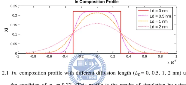
Fig. 2.1 illustrates the -dependent composition profile. We used the computing software, named “MATLAB”, to simulate the condition of .
Fig. 2.1 composition profile with different diffusion length ( = 0, 0.5, 1, 2 nm) under the condition of . (This profile is the results of simulation by using the computing software, “MATLAB”.)
2.1.2 Vacancy-Enhanced Quantum Well Interdiffusion
The atomic diffusion may be governed by either interstitials or vacancies according to their distinguishable diffusion coefficients. In this thesis, Group vacancies-dominated interdiffusion is demonstrated via taking impurity-free vacancy disordering (IFVD) as an example.
-dominated impurity-free vacancy disordering (IFVD) is found to be a two-step
mechanism, including the creation of group vacancies ( ) by out-diffusion of group -1 -0.8 -0.6 -0.4 -0.2 0 0.2 0.4 0.6 0.8 1 x 10⁻⁸ 0 0.05 0.1 0.15 0.2 0.25 In Composition Profile Xi -1 -0.8 -0.6 -0.4 -0.2 0 0.2 0.4 0.6 0.8 1 x 10⁻⁸ 1.1 1.2 1.3 1.4 1.5
Band Gap Energy Profile
x (m) E g ( e V ) Ld = 0 nm Ld = 0.5 nm Ld = 1 nm Ld = 2 nm Ld = 0 nm Ld = 0.5 nm Ld = 1 nm Ld = 2 nm
- 8 -
atoms from the semiconductor layer into the dielectric capping layer and the following diffusion of away from the dielectric film-semiconductor interface. The first step is activated by high temperature thermal treatment which leads to the thermal expansion mismatch between two adjacent layers. The generated at the interface subsequently penetrate into the underlying layers and enhance the redistribution of group atoms in the quantum well structure. As a result, the band gap profile of the semiconductor is altered.
2.1.3 SiO2-Induced InGaAs/GaAs Quantum Well Interdiffusion
is an ideal candidate for the modification of optoelectronic properties in -based structures. The / quantum well structure capped with dielectric film on the surface is investigated in this study.
The / quantum wells in our experiments are grown along direction, also called -direction in this thesis, on substrate. Two assumptions are made to simply the diffusion model. First, the stress along the growth direction is completely released during the epitaxy process, and no stress along -direction is considered. Second, the in-plane -direction and -direction are identical to produce a tetrahedral distortion.
2.1.3.1 Vacancy Generation via Thermal Treatment
Two possible factors dominate the generation of excess vacancies ( ) at the - interface. One is the solubility of atoms in the capping layer, and the other comes from the difference of the thermal expansion coefficients of and .
- 9 -
The generation of is also under the control of the dielectric film quality depending on
deposition conditions and the film thickness which controls the number of atoms that can be absorbed into the layer, yet these minor influential factors are not discussed here.
The distinctive affinity of for atoms makes it behave as a perfect solvent and absorb preferentially rather than atoms. In other words, could be seen as a sink source or a sponge that rapidly absorbs atoms up to its solubility limit.
High temperature thermal treatments are applied after the deposition of capping layer so as to build a thermal strain field which mainly results from the significantly smaller thermal expansion coefficient of than . The thermal expansion coefficient measures the fractional change in size of an object per degree change in temperature and can be written as Eq. (8).
(8)
If the thermal expansion coefficient is not a variable of temperature in the range of temperature we considered, the fractional change in volume can be calculated by the following equation.
(9)
Thermal expansion coefficients of the materials used in our experiment are listed in Table 2.1. The obvious difference of thermal expansion coefficients can be found between and while the thermal expansion coefficients of and can assumed to be identical.
After high temperature annealing, the semiconductor layers of and experience compressive strain in comparison with the tensile strain in the capping layer. The compressive strain in the layer tends to eject vacancy defects and therefore aid the movement of to penetrate into the underlying quantum well structure. The closer to the - interface, the more serious the compressive strain is. The
- 10 -
spontaneously created compressive strain gradient in the layer ensures diffuse
smoothly toward the quantum well.
Table 2.1 Thermal Expansion Coefficients [16]
Material
Thermal Expansion Coefficient
0.52
8.2
6.03
5.07
In brief, the capping layer attracts atoms to out-diffuse from the adjacent layer, and meanwhile the remaining vacancies ( ) in the layer diffuse in the opposite direction with the help of the compressive stress field. The vacancies ( ) diffused to the / quantum well make substantial contribution to the interdiffusion, and the vacancy-assisted interdiffusion mechanism will be discussed later in Section 2.1.3.3.
2.1.3.2 Strain-Dependent Vacancy Distribution
The capping layer can also play the role of patterning mask which is designed for specific apertures with various diameters. It is known that the heterostructures with dielectric capping layers behave quite distinctly from those without capping layers. The patterned samples, hence, display a two-dimensional strain profile which is in strong relation to the scheme of patterns.
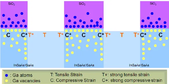
- 11 -
The excess vacancies ( ) created under the - interface are therefore
drained toward the higher compressive regions located under the layer while the adjacent strongly tensile regions located under the apertures act as barriers to this vacancy diffusion. More importantly, extremely high strain on the boundary of patterns can provide a better confinement of in the region under the layer. In Consequence, this stress-driven anisotropic diffusion in the -direction can lead to high lateral resolution of the selective area quantum well intermixing.
Figure 2.2 shows the cross-sectional strain profile in the / quantum dot structures capped with / layers [16]. and capping layers respectively contribute to compressive and tensile strain in the semiconductor layers. Also, extremely high strain is observed under the boundary of patterns.
Fig. 2.2 The cross-sectional profile of strain distribution under the patterning and capping layers [16]
- 12 -
The distribution may perfectly comply with the profile of strain field and is
schematically presented in figure 2.3. The vacancies ( ) accumulate near the - interface in the beginning of the diffusion process, and then diffuse downward the underlying layers. Because of the barrier formed by the drastic strain variation, very few
will diffuse through the boundary and toward the region without capping layers.
Theoretically, we don’t have to take into account the slight influence of the vacancy-enhanced intermixing phenomenon in the uncapped area when the lateral diffusion is minor.
Fig. 2.3 Schematic cross-sectional view of distribution obeying the strain profile
2.1.3.3 Vacancy-Assisted In-Ga Interdiffusion
In the / quantum well systems, Group -governed interdiffusion mechanism describes the movement of the diffusing components. The vacancies ( ) generated in the top layer play an important role in the diffusion of atoms. The existing vacancies reserve the position for the diffusing atoms so as to significantly
- 13 -
enhance the diffusion process. Thus, the movement should also be taken into
consideration when the / quantum well intermixing is estimated. The compositional disordering of concentration is written as the following diffusion equation.
(10)
where stands for the intrinsic diffusivity of - interdiffusion. is defined as the ratio of concentration and is the equilibrium vacancy concentration dependent on the annealing temperature.
(11)
vacancies travel throughout the samples in the manner of diffusion.
(12)
where is the diffusivity of vacancies and assumed to be constant independent of composition.
It is known that the effective diffusion coefficient ( ) for the interdiffusion is the
product of the concentration of the diffusing point defects, which indicate vacancies here, and their diffusivity.
(13)
The vacancy-enhanced diffusivity of - interdiffusion, or the effective interdiffusion diffusivity ( ), has been found to be two orders of magnitude higher than
- 14 -
2.2 Band Profile Modification via In Atom Diffusion
The energy band profiles dependent on composition ( ) and the corresponding quantized energy levels after intermixing are acquired by solving the diffusion equation and the Schrödinger equation numerically. On the assumption that diffusion obeys Fick’s second law, the post-annealed composition ( ) distribution can be simply expressed as error-function forms. Composition-dependent properties, such as effective mass, energy band gap, and stress-related coefficients, can be directly derived. Since all the parameters needed are determined, then the Schrödinger equation is possible to be solved.
In quantum mechanics, the Schrödinger equation describes how the quantum state of a physical system changes in time.
(14)
Assuming that the potential energy is invariable in time, Schrödinger equation can be simplified to the time-independent Schrödinger equation by the method of separation of variables. Approximate solutions to the time-independent Schrödinger equation are commonly used to calculate the energy levels and other properties of atoms and molecules. In a crystal, the wave function of an electron with energy E in the conduction or valence bands can be estimated by solving the following equation.
(15)
where is the wave function of the electron with effective mass ( ), and is the potential of the crystal lattice seen by the electron.
In the strained / systems, lattice-mismatch induced strain potential energy ( ) cannot be ignored when considering the potential terms in the Schrödinger equation. Actually, the Schrödinger equation is written as a more accurate form as Eq. (16)
- 15 -
The / heterostructure form a lattice-mismatched system because the lattice constant of bulk is significantly larger than the lattice constant of bulk . Built-in biaxial elastic stress is generated when the pseudomorphic layer is grown on substrate. The biaxial stress in the plane comes up with the result of hydrostatic deformation and shear deformation. The strain potential energy ( ) can be analyzed as a combination of hydrostatic stress induced energy shift ( ) and shear stress induced valence band splitting energy ( ).
(17)
where and stand for the hydrostatic deformation potential and the shear deformation potential respectively.
The hydrostatic stress influences both conduction band and valence band while only valence band is affected by the shear deformation potential which causes heavy-hole (HH) and light-hole (LH) splitting. The strain potential energy ( ) is also decided by the value of and the elastic constants ( ). The corresponding strain potential energies for conduction
band ( ) and valence band ( ) are shown in the following relations.
(18)
(19)
where is the hydrostatic deformation potential, and is the shear deformation potential.
and are the elastic stiffness constants. Strain of the epitaxial layer ( ) is defined in
Eq. (20). All the strain-related constants, including , , , , and , are dependent on composition ( ).
(20)
- 16 -
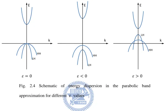
The direction of band shift depends on the sign of , and Figure 2.4 shows schematically the energy dispersion in the parabolic band approximation for different values.
Fig. 2.4 Schematic of energy dispersion in the parabolic band approximation for different values
and are known as direct band gap ( valley transition) semiconductors, and composition ( ) plays an important role in modifying the band gap of ternary alloy. ternary alloy can be regarded as a mixture of and binary compounds. The dependence of energy band gap on composition ( ) is assumed to fit a simple quadratic form.
(21)
where the so-called bowing parameter accounts for the deviation from a linear interpolation between and . The conventional value of for is in the range of 0.47 to 0.49 . E k HH LH E k HH LH E k HH LH
- 17 -
Chapter 3
Results and Discussion
3.1 Capping Layer-Induced Energy Shift via Thermal Treatment
The samples used in this study were all grown on semi-insulating substrates by a Veeco Gen II molecular beam (MBE) epitaxy system. Both and dielectric capping films, were deposited by an E-gun evaporator. In order to initiate the interdiffusion process, post-growth rapid thermal annealing (RTA) was utilized to provide high temperature circumstances up to 925 .
3.1.1 Influence of SiO2 Capping Layer
The schematic structure of sample A used to evaluate the influence of capping layer on the / quantum well intermixing is shown in Fig. 3.1. The semi-insulating GaAs substrate was first grown with a superlattice with 10 pairs of 5 nm wells and 5 nm barriers and a 100 nm buffer layer, and then it was ready to grow the designed structure. The single quantum well structure was grown as a 6 nm well sandwiched by two 6 nm barriers. The 30 nm and 1 layers were grown on the top and bottom of the / quantum well
respectively so as to provide a better confinement of electrons inside the quantum well. The top 10 nm layer protected the underlying layers from oxidized. The capping films were deposited to the thickness of 150 nm by an E-gun evaporator.
- 18 -
Fig. 3.1 The schematic epitaxy structure of sample A which was designed for a / single quantum well. The capping layer of 150 nm film was deposited on the top of the semiconductor surface.
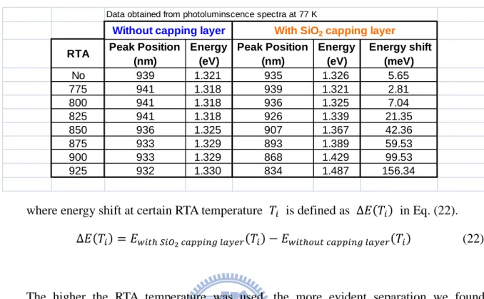
The photoluminescence spectra in this section were measured at 77 K with 488 nm argon laser as the optical pumping source. The emission wavelength of the as-grown sample is at 939 nm, and its full width at half maximum (FWHM) is about 15.2 meV. Fig. 3.2 shows the 77 K photoluminescence spectra of the samples processed at various RTA temperatures from 800 to 925 . The corresponding peak position of each sample is extracted from Fig. 3.2 and listed in Table 3.1.
- 19 -
Fig. 3.2 The photoluminescence spectra measured at 77 K. The samples were treated with rapid thermal annealing (RTA) at various temperatures (No RTA, RTA at 775, 800, 825, 850, 875, 900, 925 ). The solid lines represent the samples without capping layers while the dashed lines represent the samples with 150 nm capping layers. 800 825 850 875 900 925 950 975 1000 Wavelength (nm) No RTA N o rm a li z e d P L I n te n s it y ( a rb . u n it ) RTA775 RTA800 RTA825 RTA850 RTA875 RTA900
With SiO2 capping layer Without capping layer
RTA925
Energy Shift Influenced by SiO
- 20 -
Table 3.1 The detailed data extracted from Fig. 3.2 of sample A
where energy shift at certain RTA temperature is defined as in Eq. (22). (22)
The higher the RTA temperature was used, the more evident separation we found between the samples with capping layers and those without capping layers. The emission lengths of the samples without capping layers stayed almost the same with only slight variation. On the contrary, the samples with capping layers show drastic blue-shifts with increasing RTA temperature. That is to say, indeed enhance the quantum well intermixing, especially at higher RTA temperature. After annealing at 900 for 30 seconds, the emission peak shows a blue-shift of about 100 meV. The sample capped with and annealed at 925 indeed shows an even larger blue-shift. Yet, the peak we concerned merges with the peak around 824 nm, and this unwanted overlapping may make analysis more complicated.
In order to achieve complete disordering, the annealing time used in other approaches should be as long as several hours [22]. However, less than 1 minute is enough in the case of -enhanced quantum well intermixing. Although the annealing time we used was as short as 30 seconds, the obvious energy shift of the samples with capping layers still can be
RTA Peak Position (nm) Energy (eV) Peak Position (nm) Energy (eV) Energy shift (meV) No 939 1.321 935 1.326 5.65 775 941 1.318 939 1.321 2.81 800 941 1.318 936 1.325 7.04 825 941 1.318 926 1.339 21.35 850 936 1.325 907 1.367 42.36 875 933 1.329 893 1.389 59.53 900 933 1.329 868 1.429 99.53 925 932 1.330 834 1.487 156.34
Data obtained from photoluminscence spectra at 77 K
With SiO2 capping layer Without capping layer
- 21 -
observed. It implies that the -assisted interdiffusion rate of and atoms is substantially higher.
As for the full width at half maximum (FWHM) of the emission peak, the variation tendency with increasing RTA temperature seems to be irregular. The emission peak becomes broader when relatively lower-temperature annealing is applied, and it once again turns into a narrow peak when the annealing is processed at high temperature above 900 . The broadening may come from the non-uniform distribution of the degree of intermixing throughout the sample. Annealing below 900 can induce the interdiffusion of and atoms, but the energy provided is not large enough for all atoms move simultaneously. Higher RTA temperature not only leads to a larger blue-shift but also contributes to the uniformity in the quantum well intermixing.
3.1.2 Influence of TiO2 Capping Layer
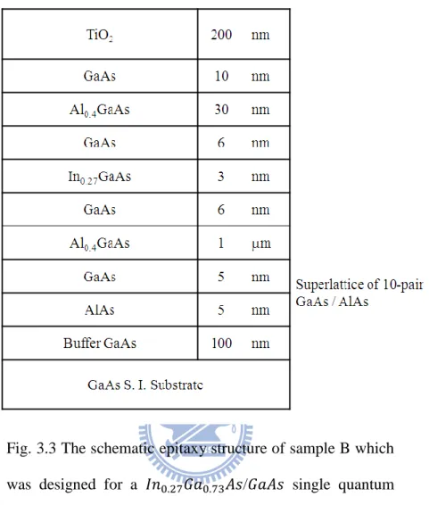
The schematic structure of sample B used to evaluate the influence of capping layer on the / quantum well intermixing is shown in Fig. 3.3. The single quantum well structure was grown as a 3 nm well sandwiched by two 6 nm barriers. Except for the quantum well design, the structure of other layers was the same as the structure in sample A. The capping films were deposited to the thickness of 200 nm by an E-gun evaporator.
films influence the quantum well intermixing in a similar manner to the capping layer but in a completely opposite way. From Table 2.1, the thermal expansion coefficient of is larger than and . Therefore, few vacancies ( ) are generated at the - interface, and the tensile strain in the top layer tends to trap vacancies and impede the interdiffusion of and atoms.
- 22 -
Fig. 3.3 The schematic epitaxy structure of sample B which was designed for a / single quantum well. The capping layer of 200 nm film was deposited on the top of the semiconductor surface.
The photoluminescence spectra in this section were measured at 25 K with 488 nm argon laser as the optical pumping source. The emission wavelength of the as-grown sample is at 914 nm, and its full width at half maximum (FWHM) is about 26.5 meV. Fig. 3.4 shows the 25 K photoluminescence spectra of the samples processed at various RTA temperatures from 850 to 900 . The corresponding peak position of each sample is extracted from Fig. 3.4 and listed in Table 3.2.
- 23 -
Fig. 3.4 The photoluminescence spectra measured at 25 K. The samples were treated with rapid thermal annealing (RTA) at various temperatures (No RTA, RTA at 850, 875, 900 ). The solid lines represent the samples without capping layers while the dashed lines represent the samples with 200 nm capping layers.
850 875 900 925 950 975 No RTA Wavelength (nm) N o rm a li z e d P L I n te n s it y ( a rb . u n it ) RTA850 RTA875 RTA900
Without capping layer
With TiO
2 capping layer
- 24 -
The capping layer functions as an inhibitor of the interdiffusion of and atoms because its relatively large thermal expansion coefficient creates tensile stress for the underlying layer. The tensile strain field limits the degree of quantum well intermixing, and an obvious energy red-shift can be found in photoluminescence spectra.
Table 3.2 The detailed data extracted from Fig. 3.4 of sample B
where energy shift at certain RTA temperature is defined as in Eq. (23). (23)
The emission peaks of the samples both with and without capping layers kept at the same position of the as-grown sample when the RTA temperature was set below 900 . The energy shift smaller than 5 meV can be seen as a negligible experimental error. When the RTA temperature was raised to 900 , the sample without capping layer had an energy red-shift of 30 meV while the sample with capping layer had a comparatively small energy red-shift of 21 meV. A meaningful energy red-shift of about 10 meV can be regarded as an evident of -impeded quantum well intermixing.
The apparent large full width at half maximum (FWHM) of the uncapped sample annealed at a middle RTA temperature of 875 can be explained as the serious non-uniformity in the degree of quantum well intermixing. By comparison, no obvious broadening is found for the samples capped with layers. The samples with capping layers show such a slight degree of quantum well intermixing that the variation of
RTA Peak Position (nm) Energy (eV) Peak Position (nm) Energy (eV) Energy shift (meV) No 914 1.357 914 1.357 0.00 850 914 1.357 911 1.361 4.47 875 914 1.357 912 1.360 2.98 900 894 1.387 900 1.378 -9.25
Data obtained from photoluminscence spectra at 25 K
With TiO2 capping layer
- 25 -
uniformity throughout the sample barely influence the FWHM of the emission peak.
In order to clearly illustrate the effects of and on the quantum well intermixing, the relation between the energy shift and the corresponding RTA temperature is plotted in Fig. 3.5. -enhanced quantum well intermixing can be inferred from the nearly exponential increase of energy shift with increasing RTA temperature. The small but meaningful energy red-shift of the sample capped with layer and annealed at 875 implies the ability of to inhibit quantum well intermixing.
Fig. 3.5 Energy shifts at various temperature induced by and capping layers. The red dots represent sample A with capping layer, and the blue triangles represent sample B with capping layer. The value of energy shift is positive for a blue-shift and negative for a red-shift.
-20 0 20 40 60 80 100 120 140 160 180 No 775 800 825 850 875 900 925 E n e rg y S h if t (m e V ) RTA Temperature (oC)
Energy Shift Induced by SiO2 / TiO2
- 26 -
3.2 Selective Quantum Well Intermixing via Patterned SiO
2Layer
For the purpose of selective area wavelength tuning of / quantum well, capping layer was patterned to be a mask. The patterning techniques used in this study were either lift-off lithography or electron-beam (e-beam) lithography. The method of e-beam lithography combined with subsequent reactive ion etching (RIE) was utilized for the fabrication of nanometer-scale patterns. Rapid thermal annealing at 875 was performed after lithography process so as to activate the quantum well intermixing mechanism. Finally, micro-photoluminescence spectroscopy (micro-PL) was used to examine the optical properties of the samples.
3.2.1 Spatial Resolution of Micro-Photoluminescence
The epitaxy structure of sample C was the same as sample B which consisted mainly of / single quantum well. Fig. 3.6 illustrates the process flow of the
fabrication of sample C with mesa patterns which are around 10 in diameter. films were deposited after photoresist (PR) coating on the surface of the semiconductor, and then lift-off lithography technique was utilized to make the mesa patterns. Afterwards, the entire sample surface was coated with films. and films used here were deposited by an E-gun evaporator and the thickness were 200 nm and 150 nm respectively.
According to the results discussed in section 3.1, the mesa patterns capped with layer performed locally impeded-quantum well intermixing. Since the layer on top of the layer had no direct contact with the underlying semiconductor, it exerted no effect on the quantum well in the regions below the mesa structures.
- 27 -
Fig. 3.6 Process flow of sample C fabrication.
From the scanning electron microscopy graphs in Fig. 3.7, the size of the hexagonal mesa patterns is about 9.5 , and the mesa structures can be easily observed. Both photoluminescence (PL) and micro-photoluminescence (micro-PL) spectra were measured for sample C. Laser beam size was the major difference between PL and micro-PL, that is to say, the area of sample surface covered in each measurement differed. The laser beam size of PL was close to 100 while the laser beam size of micro-PL was only 10 which was approximately equal to the size of mesa patterns.
When measuring PL spectra, the laser-coverage area contained both and -dominated regions. Fig. 3.7 (b) schematically shows the covered area by the PL laser beam. On the other hand, the size of micro-PL laser beam was small enough that the regions inside and outside the mesa patterns can be measured separately. In Fig. 3.7 (C), position (1) and (2) indicate two individual spectra which were measured by focusing the micro-PL laser beam on the -governed (inside the mesa) or -governed regions (outside the mesa).
TiO2
In0.27GaAs QW
SiO2
SiO2 TiO2 SiO2
In0.27GaAs QW TiO2 -film deposition d ~ 10 mm d ~ 10 mm SiO2 -film deposition Patterning by lift-off lithography As-grown sample TiO2 In0.27GaAs QW In0.27GaAs QW PR PR
- 28 -
Fig. 3.7 SEM micrographs of sample C. (a) The size of the hexagonal mesa is about 9.5 . (b) Schematic illustration of the coverage area by the PL laser beam. (c) Schematic illustration of the coverage area by the micro-PL laser beam. Position (1) and (2) indicates that the micro-PL laser beam is focused inside and outside the mesa respectively.
The photoluminescence (PL) and micro-photoluminescence (micro-PL) spectra measured at 77 K are shown in Fig. 3.8. The black line with diamond-like symbols is the PL spectrum. An emission peak with comparatively higher intensity and shorter wavelength overlaps with another emission peak with comparatively lower intensity and longer
(a)
PL Laser beam < 100 mm (2) (1) micro-PL laser beam ~ 10 mm(b)
(c)
9.41mm 9.24mm- 29 -
wavelength. The red dot dashed represents the micro-PL spectrum measured at position (1) where the layer directly contacted with layer, and the corresponding emission peak is located at 898 nm. Likewise, the blue dashed line represents the micro-PL spectrum measured at position (2) where the layer directly contacted with layer, and the corresponding emission wavelength is 916 nm.
Fig. 3.8 The photoluminescence and micro-photoluminescence spectra measured at 77 K. The upper figure combines one PL spectrum and two micro-PL spectra measured at position (1) and (2). The lower figure shows the results of peak analysis by Gaussian fitting.
850 875 900 925 950 975
PL SiO2 & TiO2 Gaussian fit peak 1 Gaussian fit peak 2
Wavelength (nm) 916 nm
Data: normalized_PLSiO2TiO2 Model: Gauss
Equation: y=y0 + (A/(w*sqrt(PI/2)))*exp(-2*((x-xc)/w)^2) Weighting: y No weighting Chi^2/DoF = 0.00001 R^2 = 0.99983 y0 0 ±0 xc1 915.82338 ±0.12427 w1 25.51908 ±0.16455 A1 14.63961 ±0.12309 xc2 898.64154 ±0.01523 w2 11.87361 ±0.04904 A2 11.88975 ±0.11205
PL SiO2 & TiO2 microPL SiO2 (1) microPL TiO2 (2) N o rm a li z e d P L I n te n s it y ( a rb . u n it ) 898 nm SiO2
SiO2 TiO2 SiO2
In0.27GaAs QW
(2)
- 30 -
The PL spectrum implies a combination of two individual peaks. Thus, we utilized the method of Gaussian fitting to analyze this multi-peak, and the detailed information is shown in the lower part of Fig. 3.8. Two individual peaks located at 898.6 nm and 915.8 nm were extracted from the PL spectrum, and these two wavelengths perfectly agree with those two emission peaks in the micro-PL spectra.
All in all, micro-PL provides better spatial resolution than PL because the laser beam shrinks in size when passing through objective lens. If the emission wavelengths from the regions inside and outside the patterns are too close to be distinguished, micro-PL is the better alternative to investigate selective area interdiffusion.
3.2.2 Aperture Size-Dependent Energy Shift
Semiconductor properties can be quite different when the scale is down to nano-meter. In this section, we concentrate on the influence of aperture size on the patterned- -induced energy shifts. Nano-meter scaled apertures were patterned on the capping layers.
As mentioned in section 3.1, the energy shift caused by capping layer at RTA temperature of 875 can barely be distinguished, although indeed made contribution to inhibiting FWHM from broadening. For the sake of practicability and convenience during the fabrication of nanometer-scaled patterns, we skipped the procedure of deposition and replaced lift-off lithography with e-beam lithography and reactive ion etching (RIE). The structure of the sample used here is the same as sample A, including the epitaxy structure and the growing condition of capping layers. The fabrication process flow is illustrated in Fig. 3.9.
- 31 -
The capping layer was patterned with circular apertures in various diameters (d = 55, 75, 100, 125, 135 nm). The apertures with the same diameter were arranged in an array, of which the periodicity is 200 nm.
Fig. 3.9 Process flow of patterning capping layer by e-beam and RIE.
SiO2 In0.22GaAs QW SiO2 -film deposition d ~ nm Patterning by ebeam & RIE As-grown
sample
SiO2 In0.22GaAs QW In0.22GaAs QW
- 32 -
Scanning electron microscopy (SEM) was used to examine the diameter of apertures. The SEM pictures in Fig. 3.10 display two arrays, of which the diameter of apertures is 75 nm and 100 nm repectively.
Fig. 3.10 SEM micrographs of the patterns on the capping layers. (a) and (b) shows the circular apertures are 75 nm and 100 nm in diameter respectively. The periodicity of both (a) and (b) is 200 nm.
(a)
(b)
75.0nm 72.8nm 76.1nm 101.5nm 101.5nm 102.6nm 100.4nm- 33 -
The patterned samples were annealed at RTA 875 and 900 and measured by micro-photoluminescence (micro-PL) at 77 K shown in Fig. 3.11. Since the size of designed patterns (d is in the range of 55 nm to 135 nm) was much smaller than the micro-PL laser beam size (10 ), inevitably the area both inside and outside apertures were covered by the laser beam. Theoretically, two emission peaks should exist concurrently in a micro-PL spectrum. The higher-energy peak stands for the area outside apertures while the lower-energy peak stands for the area inside apertures. However, general semiconductor properties suggest that electrons prefer staying at lower-energy states and the diffusion length of electrons in can be larger than 5 . As a result, electrons not only move toward but also accumulate in the regions inside apertures, and then only few electrons remaining outside apertures can contribute to the emission in the higher-energy state. The emission peak we concerned is the lower-energy one which emitted from the regions inside apertures, where the capping layer is removed completely and -induced quantum well intermixing should not happen.
In an idea case or the case considering micrometer-scaled apertures, no obvious energy shift would be found in the regions inside apertures. It implies that vacancies in the adjacent regions under capping layer hardly diffuse across the boundary. That would totally not be the case when the size of apertures is scaled down to nanometer.
vacancies ( ) diffuse downward to / quantum well and induce the interdiffusion of and atoms. In the meantime, vacancies ( ) diffuse laterally toward the adjacent regions without capping layer as well. As a consequence, the regions inside apertures is also affected by quantum well intermixing. When the size of apertures is getting small, the lateral diffusion effect becomes more influential. Presumably, the effective diameter of apertures is limited to a specific minimum value for each RTA temperature. That is to say, if the diameter of apertures is smaller than the effective minimum, all of the regions inside apertures will suffer quantum well intermixing thoroughly and
- 34 -
aperture-influenced selective area quantum well intermixing will no longer be valid.
In the case of RTA 875 , the emission peak from the regions capped with non-patterned layer was located at 893 nm equivalent to 1.389 eV, and the emission peak from the sample uncapped with layer is located at 933 nm equivalent to 1.329 eV. The aperture-dependent energy shifts can be easily found from the micro-photoluminescence spectra shown in Fig. 3.11. When the diameter is getting smaller, the emission peak from the regions inside apertures becomes closer to the peak from the regions capped with non-patterned layer.
Fig. 3.11 The micro-photoluminescence spectra measured at 77 K. The orange solid curve represents the sample capped with non-patterned capping layer. The blue solid line represents the sample without capping layer. The lines with symbols (pink squares, red circles, and green triangles) represent the patterned samples (d = 75, 100, 125 nm). 1.28 1.32 1.36 1.40 1.44 0.0 0.2 0.4 0.6 0.8 1.0
Without SiO2 capping layer d = 125 nm
d = 100 nm d = 75 nm
With non-patterned SiO2 layer
N o rm a li z e d P L I n te n s it y ( a rb . u n it ) Energy (eV)
- 35 -
The energy shift of the sample with apertures in a specific diameter is equal to its emission energy minus the emission energy of the sample without capping layer annealed at the same RTA temperature, shown in Eq. (24).
(24)
In Fig. 3.12, the red short-dashed line indicates the highest energy-shift level of the samples with capping layer annealed at 875 . Similarly, the green dot-dashed line indicates the highest energy-shift level of the samples with capping layer annealed at 900 .
In the case of RTA 900 , the emission peak from the regions capped with non-patterned layer was located at 862 nm equivalent to 1.439 eV, and the emission peak from the sample uncapped with layer is located at 933 nm equivalent to 1.329 eV.
Fig. 3.12 Diameter-dependent energy shifts of the patterned samples annealed at 875 and 900 . The lines and circular symbols in red color represent the samples annealed at 875 . The lines and triangular symbols in green color represent the samples annealed at 900 .
With non-patterned SiO2capping layer
@ RTA 875 oC With non-patterned
SiO2capping layer @ RTA 900 oC 0 20 40 60 80 100 120 0 20 40 60 80 100 120 140 160 E n e rg y S h if t (m e V ) Diameter (nm) RTA875 No Pat @ RTA875 RTA900 No Pat @ RTA900
- 36 -
According to section 3.1.1, we know that the degree of quantum well intermixing becomes greater as the RTA temperature increases. In Fig. 3.12, the samples annealed at 900 show an even more severe effect of aperture-dependent energy shift. It implies that the case of RTA 900 , in which the minimum effective diameter is 75 nm, cannot achieve the goal of three-dimensional (3D) quantum dot (QD) confinement. The self-assembled QDs grown by a Veeco Gen II molecular beam (MBE) epitaxy system in our laboratory are 40nm to 60 nm in diameter. For this reason, we expect that the fabrication of artificial quantum dot confinement is possible to accomplish when the minimum effective diameter can be controlled under 50 nm. From the curve of RTA 875 in Fig. 3.12, we infer that it may be feasible to design apertures with diameter smaller than 50 nm under the condition of applying rapid thermal annealing at 875 .
Fig. 3.13 Schematic of three-dimensional (3D) confinement by selective area / quantum well intermixing. The lateral potential profiles were simulated for different degree of lateral diffusion.
GaAs
InGaAs
GaAs
Patterned SiO2capping layer QD effectGaAs substrate
3-D confinement -1 -0.8 -0.6 -0.4 -0.2 0 0.2 0.4 0.6 0.8 1 x 10⁻⁸ 0.75 0.8 0.85 0.9 0.95 1 x (m) V c + S c ( e V ) Severe VGalateral diffusion- 37 -
The basic idea of artificial quantum dot confinement fabricated by the method of selective area quantum well intermixing is illustrated in Fig. 3.13. In-plane ( plane) lateral potential can be established by the use of patterned capping layer while the interdiffusion along the growth-direction ( -direction) leads to vertical potential. A three-dimensional (3D) confined potential is then created under the regions inside apertures.
The production of quantum dots by selective interdiffusion has already been reported in / quantum well system[23]. This successful case reinforces our confidence in the possibility of artificial quantum dot manufactured in / quantum well system.
3.2.3 Excitation Power-Dependent Emission Peak
Photoluminescence spectra strongly depend on the excitation power, and the spectra obtained by applying various excitation powers can be drastically different even if the identical sample is measured. Excitation power density is directly associated with
pumped-electron density in the measurement. The structure of the sample used in this section is the same as sample A, including the
epitaxy structure ( / single quantum well) and the growing condition of capping layers. The capping layer was patterned as an array of circular apertures. The diameter and the periodicity of the circular apertures are 50 nm and 500 nm respectively (d = 75 nm; P = 500 nm). Fig. 3.14 shows the schematic illustration of the patterned capping layer. Rapid thermal annealing at 875 for 30 seconds is performed before the micro-photoluminescence (micro-PL) measurement at 77 K.
- 38 -
Fig. 3.14 Schematic of the pattern designed as an array of circular apertures. The diameter of the circular apertures is 75 nm, and the periodicity is 500 nm. (d = 75 nm; P = 500 nm)
Fig. 3.15 shows the micro-photoluminescence (micro-PL) spectra measured at 77 K, and each curve represents one excitation power. In order to investigate the transformation of PL spectrum with increasing excitation power, the magnitude of PL intensity in each spectrum was not normalized. Furthermore, all of the experimental conditions and parameters, only except for excitation power, were kept identical, and thus the comparison is convincing.
Higher excitation power undoubtedly pumps more electrons to the sample, and more electrons contribute to larger PL intensity. Nonetheless, the magnification of the emission peak at about 1.33 eV does not follow a uniform scale-up tendency. As excitation power increases, the peak shape gets further away from Gaussian distribution. The emission peak expands more enormously toward the higher-energy side and shows a shoulder-like side peak. If applying even higher excitation power, another peak appears at around 1.45 eV.
- 39 -
Fig. 3.15 The power-dependent micro-photoluminescence spectra of the sample with patterned capping layer (d = 75 nm; P = 500 nm).
It is well-known that electrons tend to fill in the unoccupied lowest-energy states. Therefore, we suggest that energy states in a material can be explored with the help of high excitation power which provides sufficient electrons.
To give a logical and reasonable explanation how the PL emission peak evolves, we propose a demonstration from the points of view both in the energy space and in the real space. There are two major groups of energy states in our system, including a higher-energy one (group A) and a lower-energy one (group B). Lower-energy states of group A come from the regions inside apertures while the -capped regions outside apertures contribute to higher-energy states of group B. Density of states as a function of energy is schematically depicted in Fig. 3.16. 1.25 1.30 1.35 1.40 1.45 1.50 1.55 0 5 10 15 20 25 30 35 40 45 50 Increasing excitation power 0.60 mW (10) 1.20 mW (20) 1.80 mW (30) 2.40 mW (40) 3.00 mW (50) 3.30 mW (55) 3.36 mW(56) 3.42 mW (57) 3.48 mW (58) 3.54 mW (59) 3.60 mW (60) P L I n te n s it y ( a rb . u n it ) Energy (eV) GaAs
- 40 -
Fig. 3.16 Schematic of density of states (DOS). The blue line labeled as “Group A” corresponds to the regions inside apertures while the orange line labeled as “Group B” corresponds to the regions outside apertures. The area outside the apertures is covered with films.
Table 3.3 schematically demonstrates the gradual evolution of the transformation in the PL spectra. Electrons pumped to the / heterostructure are assumed to obey Fermi-Dirac distribution. In the first column, which is derived from the energy space, Fermi-Dirac distribution of electrons shows its position in relation to density of states and is presented as green dashed line. In the second column, which is derived from the real space, distribution of electrons is associated with excitation power density. Pumped electrons first fill in the lower-energy regions inside apertures, and then excess electrons, provided by increasing excitation power density, flow outward to the higher-energy regions capped with layer. Combining the phenomena occurred in the energy space and the real space, the corresponding micro-photoluminescence spectra are shown in the third column.
- 41 -
The photoluminescence spectra are classified into four stages illustrated in Table 3.3. As for stage (I), the excitation power is so low that only small part of ground states in group A is filled. In this case, all the pumped electrons are confined in the regions inside apertures. As a consequence, only one emission peak can be observed and the full with at half maximum (FWHM) is narrow.
In stage (II), more electrons allowed to occupy relatively higher-energy levels give the result that larger part of ground states in group A is filled. The pumped electrons occupying the relatively higher-energy ground states in group A lead to the non-uniform broadening, as known as Fermi-filling of the 2-D step-like DOS in quantum well systems.
When the excitation power of stage (III) is getting much higher, some electrons may fill in the excited states of group A and result in a shoulder-like side peak at around 1.401 eV. At the same time, few pumped electrons with even higher energy move towards the regions outside apertures which correspond to the ground states of group B. That is to say, the distribution of pumped electrons is expanding across the boundary of apertures. A higher-energy peak coming from group B turns out to appear at 1.450 eV.
In the final stage (IV), the ground states of group A are completely filled, and thus the PL intensity of the emission peak at 1.33 eV no longer increases. All of the excessively pumped electrons make contribution to magnifying the PL intensity of the excited states of group A and the ground states of group B. We can tell from the increase of the emission peak at 1.450 eV that the distribution of pumped electrons keeps expanding outwards and more regions outside apertures are covered. In the real space, the electron diffusion length in -based semiconductor materials can be several while both the size of diameter and periodicity is less than 1 . On this basis, the electrons pumped to the sample surface can move freely between group A (inside the apertures) and group B (outside the apertures) in the real space and perfectly follow the rules in the energy space.
- 42 -
Table. 3.3 Distribution of electrons and the corresponding PL spectrum
Energy Space Real Space Corresponding PL Spectrum
Group A Group B 1.25 1.30 1.35 1.40 1.45 0 5 10 15 20 25 30 35 40 45 50 0.60 mW (10) P L I n te n s it y ( a rb . u n it ) Energy (eV) Group A Group B 1.25 1.30 1.35 1.40 1.45 0 5 10 15 20 25 30 35 40 45 50 2.40mW (40) P L I n te n s it y ( a rb . u n it ) Energy (eV) Group A Group B 1.25 1.30 1.35 1.40 1.45 0 5 10 15 20 25 30 35 40 45 50 3.42 mW (57) P L I n te n s it y ( a rb . u n it ) Energy (eV) 1.336 1.401 1.450 Group A Group B 1.25 1.30 1.35 1.40 1.45 0 5 10 15 20 25 30 35 40 45 50 3.60 mW (60) P L I n te n s it y ( a rb . u n it ) Energy (eV) 1.336 1.401 1.450 (I) (II) (III) (IV)
![Table 2.1 Thermal Expansion Coefficients [16]](https://thumb-ap.123doks.com/thumbv2/9libinfo/8060090.162926/19.892.252.681.238.519/table-thermal-expansion-coefficients.webp)
![Figure 2.2 shows the cross-sectional strain profile in the / quantum dot structures capped with / layers [16]](https://thumb-ap.123doks.com/thumbv2/9libinfo/8060090.162926/20.892.196.731.568.999/figure-sectional-strain-profile-quantum-structures-capped-layers.webp)