planar-gate structures
Yung-Chiang Lan, Chun-Tao Lee, Yuan Hu, Shih-Hung Chen, Cheng-Chung Lee, Bing-Yue Tsui, and Tsang-Lang Lin
Citation: Journal of Vacuum Science & Technology B 22, 1244 (2004); doi: 10.1116/1.1710488 View online: http://dx.doi.org/10.1116/1.1710488
View Table of Contents: http://scitation.aip.org/content/avs/journal/jvstb/22/3?ver=pdfcov Published by the AVS: Science & Technology of Materials, Interfaces, and Processing
Articles you may be interested in
Novel tapered macrogate structure for carbon nanotube based field emission display J. Vac. Sci. Technol. B 27, 1097 (2009); 10.1116/1.3125278
Toward a lateral carbon nanotube based field emission triode J. Vac. Sci. Technol. B 26, 838 (2008); 10.1116/1.2805248
Study of high-brightness flat-panel lighting source using carbon-nanotube cathode J. Vac. Sci. Technol. B 26, 106 (2008); 10.1116/1.2825145
Study of the triode structure in a field emission display element J. Vac. Sci. Technol. B 24, 962 (2006); 10.1116/1.2183782
Modeling of emitted current distribution and electron trajectories in the thin-film field-emission triode J. Vac. Sci. Technol. B 22, 1250 (2004); 10.1116/1.1736636
with under-gate and planar-gate structures
Yung-Chiang Lana)
Institute of Electro-Optical Science and Engineering, National Cheng Kung University, No. 1, Ta-Hsueh Road, Tainan 701, Republic of China
Chun-Tao Lee
Electronics Research and Service Organization, Industrial Technology Research Institute, E1100 ERSO/ITRI, Chutung, Hsinchu, Taiwan 310, Republic of China
Yuan Hu
Department of Engineering and System Science, National Tsing-Hua University, Hinchu, Taiwan 300, Republic of China
Shih-Hung Chen
Department of Physics, National Changhua University of Education, Changhua 500, Republic of China
Cheng-Chung Lee
Electronics Research and Service Organization, Industrial Technology Research Institute, E1100 ERSO/ITRI, Chutung, Hsinchu, Taiwan 310, Republic of China
Bing-Yue Tsui
Department of Electronics Engineering, National Chiao-Tung University, Hinchu, Taiwan 300, Republic of China
Tsang-Lang Lin
Department of Engineering and Systems Science, National Tsing-Hua University, Hinchu, Taiwan 300, Republic of China
共Received 6 October 2003; accepted 23 February 2004; published 1 June 2004兲
Recently, two new CNTs-based triode structures, i.e., under-gate and planar-gate structures, for field emission display were proposed and exhibited good characteristics. In this paper, we will investigate how the current density distributed on anode plate and how the display’s resolution affected by the bias conditions of the emitter and the gate electrode via computer simulation. Our simulation results exhibit that the gate voltage has a strong effect on display’s resolution. For the planar triode structure, the good resolution is achieved when the gate voltage is adjusted to converge the electron beams on an anode plate. For the under-gate structure, the display has a good resolution provided that the gate voltage is not too large to pull the electrons striking on other pixels. In general, the under-gate structure has a wider gate-biased operating condition, but the planar triode structure has a higher light efficiency under the same resolution. Due to the lack of field effect in the y -direction, the spot size of the current density on anode plate looks like strips instead of points. And the resolution of the display will be affected by this factor. © 2004 American Vacuum Society.
关DOI: 10.1116/1.1710488兴
I. INTRODUCTION
The discovery of carbon nanotubes 共CNTs兲 has drawn a lot of attention due to their unique physical properties and various potential applications.1–5 Due to their high aspect ratios and small radii of curvature, CNTs exhibit excellent field emission characteristics. A high field emission current density of 10 mA/cm2and low turn-on electric field of 0.75– 0.8 V/m have been reported,6,7 which are very advanta-geous for flat panel display applications. In field emission display 共FED兲 design, the triode structures are more attrac-tive for their lower driving voltage and higher light effi-ciency. Recently, two new CNTs-based triode structures, i.e., under-gate8 and planar-gate9structures, for FEDs were pro-posed and exhibited good characteristics. In such types of
FEDs, the lateral gate electrode generates the transverse elec-tric fields to pull out the electrons from the neighboring emit-ters. And for the planar-gate structure, the electron beams emitting from the edges of two neighboring emitters can con-verge on an anode plate to improve the resolution of the display under some bias conditions of the gate electrode. In this paper, the computer simulation studies of such triode-structure CNT-FEDs were carried out to investigate the ef-fects of the gate voltage upon the current density distribution and the convergence of the electron beams on an anode plate. The simulation model and method is described in Sec. II of this article. In Sec. III, the simulation results and discus-sions are given. Finally, the concludiscus-sions are given in Sec. IV. II. SIMULATION METHOD
A particle-in-cell computer simulation code MAGIC共Ref. 10兲 was used for this study. MAGIC is a three-dimensional,
finite-difference, time domain code for self-consistent simu-lation of the electromagnetic fields and charged particles. The electromagnetic fields are advanced in time at each time step. In each time step, the charged particles are moved ac-cording to the Lorentz equation using the fields advanced in each time step. The weighted charge density and current den-sity at the grids are subsequently calculated. The obtained charge density and current density are subsequently used as sources in the Maxwell equations for advancing the electro-magnetic fields.
In the field emission process, electron emission is mod-eled by the Fowler–Nordheim共F–N兲 equation as
J⫽AE 2
t2 exp
冉
⫺B共y兲3/2
E
冊
, 共1兲where A⫽1.5415⫻10⫺6, E is the normal component of the electric field at the emitter surface,is the work function of the emitter, B⫽6.8308⫻109, t2 is taken as approximately 1.1, and(y )⫽0.95⫺y2 with y⫽3.79⫻10⫺5⫻E1/2/ in SI units. The MAGIC code provides a F–N equation module to simulate the field emission. Initially, the electrostatic field along the emitter surface is determined for a given geometry and applied voltages. The emission charge is determined by Eq. 共1兲 according to the local electric field. The simulation proceeds by pushing the emitted electrons, weighting the current and charge densities to the grids, updating the elec-tromagnetic fields, and calculating the emission charges. These processes are repeated for each time step until the specified number of time steps is reached. The space-charge effects are automatically included in such a simulation algo-rithm.
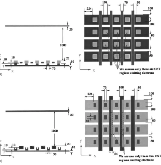
The configurations of under-gate and planar-gate type FEDs investigated in this study are shown in Fig. 1. The Cartesian x – y – z coordinate system is adopted in this simu-lation study. The simusimu-lation domain and the geometry pa-rameters are shown in Fig. 2. Due to the extremely small dimension of the carbon nanotubes, it is impractical to pre-cisely model every nanotube in the whole display structure. Instead, we model the emitter as a thin film electrode and adjust the work function of the artificial emitter to approxi-mate the real nanotube emission current. In our study, the voltage difference between cathode and anode is set to 2000 V. The voltage differences between cathode and gate are set to 30 V, 90 V, 150 V, and 210 V. And the value of the work function used in the simulation is set to 0.095 eV.
III. RESULTS AND DISCUSSIONS
For illustrating clearly the effects of the gate voltage upon the current density distribution and the convergence of the electron beams on anode plate, we compare the simulation results of the electron trajectories, the current distributions on anode plate and the equal-potential contours at the same time for different gate voltages. Figure 3 shows the simula-tion results of the 3D electron trajectories of the planar-gate CNT-FED device at the emitter voltage of 0 V, the anode voltages of 2000 V, and the gate voltage of 90 V, 150 V, and 210 V, respectively. The geometry and dimension of the
simulated triode-type CNT-FED device have been depicted in Sec. II. The corresponding current density distributions on anode plates and the equal-potential contours on x – z plane are shown in Figs. 4 and 5, respectively. As shown in Figs. 3, Fig. 4, and Fig. 5, the gate electrode attracts the electrons emitting from its neighboring 共left- and right-side兲 CNT emitters in the x-direction. For the 90-V-gate-voltage case
关Fig. 3共a兲, Fig. 4共a兲, and Fig. 5共a兲兴, the attracting force from
gate is not enough strong that the electron beams from the edges of left- and right-side emitters cannot, converge on an anode plate共in the x-direction兲. Therefore two lighting strips will appear in the same pixel of the screen due to the non-converged electron beams, and the resolution of the display will be not good under this bias condition. When the gate voltage is 150 V, as shown in Fig. 3共b兲, Fig. 4共b兲, and Fig. 5共b兲, the electron beams from the edges of left- and right-side emitters can converge on an anode plate 共in the x-direction兲. And the resolution of the display will become better. When the gate voltage is increased to 210 V, as shown in Fig. 3共c兲, Fig. 4共c兲, and Fig. 5共c兲, the gate’s attractive force becomes too strong that the linewidths along the x FIG. 1. Schematic of共a兲 planar-gate and 共b兲 under-gate CNT-FED structures.
direction are larger. In this case, the display’s resolution will becomes poor again. It can also be found that, from Fig. 3 and Fig. 4, due to lack of attracting fields in the y -direction, the electrons beams emitting from the edges of two neigh-boring emitters cannot converge in this direction. And the current density distributions look like strips instead of points on anode plates.
Figure 6 shows the simulation results of the 3D electron trajectories of the under-gate CNT-FED device at the gate voltage of 0 V, the emitter voltages of⫺90 V, ⫺150 V, and
⫺210 V, respectively, and the anode voltage of 1910 V,
1850 V, and 1790 V, respectively. And the corresponding current density distributions on anode plates and the equal-potential contours on the x – z plane are shown in Fig. 7 and Fig. 8, respectively. From Fig. 6, Fig. 7, and Fig. 8, it can be found that, the gate electrode only exerts an attractive force to electrons emitting from left-side emitters. Therefore, there is no need to adjust the voltage difference between emitter and gate to converge the electrons 共in the x-direction兲. And
FIG. 3. Three-dimensional electron trajectories of the planar-gate structure with emitter voltage of 0 V, anode voltage of 2000 V, and gate voltage of共a兲 90 V, 共b兲 150 V, and 共c兲 210 V, respectively.
FIG. 2. Schematic of simulation domain and geometrical parameters used in the simulation,共a兲 planar-gate, and 共b兲 under-gate structures. The units are inm.
FIG. 4. Current density distributions on anode plate of the planar-gate structure with emitter voltage of 0 V, anode voltage of 2000 V, and gate voltage of共a兲 90 V,共b兲 150 V, and 共c兲 210 V, respectively.
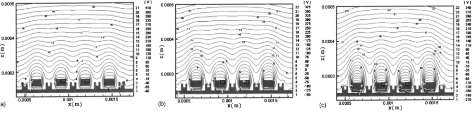
FIG. 5. Equal potential contours on the x – z plane of the planar-gate structure with emitter voltage of 0 V, anode voltage of 2000 V, and gate voltage of共a兲 90 V,共b兲 150 V, and 共c兲 210 V, respectively.
FIG. 6. Three-dimensional electron trajectories of the under-gate structure with gate voltage of 0 V and共a兲 emitter voltage of ⫺90 V, anode voltage of 1910
V,共b兲 emitter voltage of ⫺150 V, anode voltage of 1850 V, and 共c兲 emitter voltage of ⫺210 V, anode voltage of 1790 V, respectively.
FIG. 7. Current density distributions on the anode plate of the under-gate structure with gate voltage of 0 V and共a兲 emitter voltage of ⫺90 V, anode voltage of 1910 V,共b兲 emitter voltage of ⫺150 V, anode voltage of 1850 V, and 共c兲 emitter voltage of ⫺210 V, anode voltage of 1790 V, respectively.
in general, the resolution of the display is not bad 共in the x-direction兲 provided that the negative emitter voltage is not too large to pull the electrons striking on other pixels. But similar to the planar-gate case, due to lack of attracting fields in the y -direction, the current density distributions look like long strips on anode plates.
Figure 9 shows the current density distributions along the x-direction at y⫽0.0011 m and on anode plate for planar-gate关Fig. 9共a兲兴 and under-gate 关Fig. 9共b兲兴 structure devices.
It can be found clearly that, for the planar-gate structure, the current density profiles converge to single peaks gradually when the gate voltage is increased from 30 V to 150 V. But when the gate voltage is increased more共from 150 V to 210 V兲, the single current density profile becomes wider. For the under-gate structure, the current density profiles along the x-direction become wider monotonically as the negative emitter voltage is increased. One can also find, from the comparison between Fig. 9共a兲 and Fig. 9共b兲, that the planar-gate structure has a higher light efficiency than the under-gate structure under the same display’s resolution.
IV. CONCLUSIONS
Our simulation results exhibit that for the planar-gate structure, the gate voltage has a stronger effect on the dis-play’s resolution. The good resolution is achieved only when the gate voltage is adjusted to converge the electron beams on an anode plate. For the under-gate structure, the display has a good resolution provided that the gate voltage is not too large to pull the electrons striking on other pixels. In general, the under-gate structure has a wider gate-biased op-erating condition, but the planar triode structure has a higher light efficiency under the same resolution. Due to the lack of field effect in the y -direction, the spot size of the current density on the anode plate looks like strips instead of points. So the resolution of the display will be affected by this fac-tor.
ACKNOWLEDGMENTS
The authors would like to acknowledge the National Cen-ter for High-Performance Computing for providing the MAGICcode and computer facilities.
1S. Iijima, Nature共London兲 354, 56 共1991兲.
2A. G. Rinzler, J. H. Hafner, P. Nikolaev, L. Lou, S. G. Kim, D. Tomanek, P. Nordlander, D. T. Colbert, and R. E. Smalley, Science 269, 1550 共1995兲.
3W. A. de Herr, A. Chatelain, and D. Ugarte, Science 270, 1179共1995兲. 4P. G. Collins and A. Zettl, Phys. Rev. B 55, 9391共1997兲.
5S. Fan, W. Liang, H. Dang, N. Franklin, T. Tombler, M. Chapline, and H. Dai, Photonics Spectra 8, 179共2000兲.
FIG. 8. Equal potential contours on the x – z plane of the under-gate structure with gate voltage of 0 V and共a兲 emitter voltage of ⫺90 V, anode voltage of 1910
V,共b兲 emitter voltage of ⫺150 V, anode voltage of 1850 V, and 共c兲 emitter voltage of ⫺210 V, anode voltage of 1790 V, respectively.
FIG. 9. Current density distributions along the x-direction at y⫽0.0011 m and on the anode plate for共a兲 planar-gate and 共b兲 under-gate structures with different emitter-to-gate voltage.
6Q. H. Wang, T. D. Corrigan, J. Y. Dai, R. P. H. Chang, and A. R. Krauss, Appl. Phys. Lett. 70, 3308共1997兲.
7A. M. Rao, D. Jacques, R. C. Haddon, W. Zhu, C. Bower, and S. Jin, Appl. Phys. Lett. 76, 3813共2000兲.
8M. Kim et al., IDMC 2002. 9
C. T. Lee et al., SID2003 Digest 24.4, 2003.
10B. Goplen, L. Ludeking, D. Smithe, and G. Warren,
MAGIC User’s Manual, Mission Research Corp., MRC/WDC-R-409共1997兲.