國立交通大學
電子工程學系 電子研究所碩士班
碩士論文
多晶矽奈米線薄膜電晶體之研製與應用於酸鹼
感測器之研究
Fabrication, Characterization, and pH Sensors
Application of Poly-Si Nanowire Thin Film Transistors
研 究 生:陳冠智
指導教授:林鴻志 博士
黃調元 博士
多晶矽奈米線薄膜電晶體之研製與應用於酸鹼
感測器之研究
Fabrication, Characterization, and pH Sensors
Application of Poly-Si Nanowire Thin Film Transistors
研 究 生:陳冠智 Student: Kuan-Chih Chen 指導教授:林鴻志 博士 Advisors: Dr. Horng-Chih Lin 黃調元 博士 Dr. Tiao-Yuan Huang
國立交通大學
電子工程學系 電子研究所碩士班
碩士論文
A Thesis
Submitted to Department of Electronics Engineering & Institute of Electronics College of Electrical and Computer Engineering
National Chiao-Tung University in Partial Fulfillment of the Requirements
for the Degree of Master in
Electronic Engineering July 2010
Hsinchu, Taiwan, Republic of China
i
多晶矽奈米線薄膜電晶體之研製與應用於酸鹼感測器
之研究
研 究 生:陳冠智 指導教授:林鴻志 博士
黃調元 博士
國 立 交 通 大 學
電子工程學系 電子研究所碩士班
摘要
我們成功的發展出一套簡單與低成本的技術,來製作奈米線場效電晶體。藉 由此種元件,我們可以得到一個接近理想狀態的酸鹼感測器(57.1mV/pH)。此外, 我們可以不需藉由任何額外的外接電路,即可觀測出酸鹼溶液所造成的即時電性 變化,同時,此項元件還能多次重覆使用。 另外,我們也比較了奈米線與一般的平面場效電晶體電特性上的差異,以及 感測的敏感度表現。我們發現,相較於傳統電晶體的次臨界擺幅(1333 mV/dec), 奈米線改進的幅度相當大(297 mV/dec)。此外,對於感測器方面,奈米線所產生 的電流敏感度(12.78%/pH)也比傳統電晶體(5.46%/pH)的表現為好。而這些特性 也間接證明了本實驗室所製作出的奈米元件特性優異,非常適合用於感測器方 面。ii
Fabrication, Characterization, and pH Sensors
Application of Poly-Si Nanowire Thin Film Transistors
Student:Kuan-Chih Chen Advisors:Dr. Horng-Chih Lin
Dr. Tiao-Yuan Huang
Department of Electronics Engineering & Institute of Electronics
National Chiao Tung University
Abstract
In this thesis, we’ve successfully developed a simple and low-cost method to fabricate thin film transistors with nanowire channels. By employing the fabricated
devices equipped with a SiO2 sensing pad for pH sensing application, a high
sensitivity (57.1mV/pH) is obtained, which is close to the ideal value (60mV/pH).
Besides, real-time drain current response corresponding to the variation of pH value
in the test solution is demonstrated without using any external circuit. Reproducibility
of such capability is also confirmed in this work.
We’ve also investigated and compared the basic and pH sensing characteristics of the nanowire structures and conventional planar devices. The subthreshold swing
of the nanowire structures (297 mV/dec) is much better than that of the planar ones
iii
(12.78%/pH) is also better than that of the planar (5.46%/pH) one. These
iv
Acknowledgement
兩年的歲月很快就過去了,當中不管是酸、甜、苦、辣,皆是我一輩子難忘 的回憶,首先要感謝林鴻志教授以及黃調元教授,謝謝老師在這兩年辛苦的教 導,以及在學生論文上所投入的心力,謝謝。 再來就是要感謝各位學長姐,徐博、大師、蔡子儀、阿民、MACA、阿毛、 克慧等等,謝謝你們,不管是在製程上以及理論上,甚至是論文以及口試都給了 我很大的幫助,真的很感謝你們呦! 另外,還要感謝的就是身邊的同學們,峰哥、家維、白正瑋、小輔子、冠宇、 張媽以及張博翔,謝謝你們所帶給我的每一個歡樂時光,我都會永遠記得的,還 有一個不能忘記的就是生科的學妹喔,謝謝你,否則這本論文就完成不了了。 再來一定不能忘記要感謝的,那就是爸爸和媽媽啦,謝謝你們的養育之恩, 讓我在讀書上沒有後顧之憂,也感謝你們的支持,讓我在人生的道路上,教導我 很多待人處事的道理,我想這份恩情我會好好的回報的,最後要感謝的是小豬, 謝謝妳在我身邊的陪伴,讓我的人生有了新的方向。v
Contents
Abstract ... i
Acknowledgement ... iv
Contents ... v
Table Captions ... vii
Figure Captions ... viii
Chapter 1 Introduction ... 1
1-1 An Overview of Nanowire Technology ... 1
1-1-1 Bottom-Up Approach ... 2
1-1-2 Top-Down Approach ... 3
1-2 Introduction of Sensor Devices ... 4
1-2-1 Introduction of ISFET ... 4
1-3 Motivation ... 5
1-4 Organizations of the Thesis ... 7
Chapter 2 Device Structures, Fabrication and Characteristic Analysis ... 8
2-1 Process Flow and Structure of NW Devices ... 8
2-2 Process Flow and Structure of Planar Devices... 11
2-2-1 Planar Device with Thin Channel ... 11
2-2-2 Planar Device with Thick Channel ... 12
2-3 Measurement Setups and Electrical Characteristics of the Fabricated Devices ... 13
2-3-1 Measurement System ... 13
2-3-2 Theory and Model of Threshold Voltage Variation ... 13
2-3-3 Comparisons of Basic Electrical Characteristics ... 16
Chapter 3 Analysis of the Characteristics of pH Sensors ... 21
vi
3-2 The Theory of pH Sensors ... 23
3-3 Analysis of pH Sensing Characteristics ... 25
3-3-1 The Sensitivity of Different Structures ... 25
3-3-2 Effects of Antenna Pad Area ... 27
3-3-3 Effects of Antenna Pad Materials ... 28
Chapter 4 Conclusion and Future Work ... 31
4-1 Conclusion ... 31 4-2 Future Work ... 32 References ... 34 Tables ... 42 Figures ... 43 Vita ... 86
vii
Table Captions
Chapter 2
Table 2-1 summarize of the electrical characteristics for the devices ... 42
Chapter 3
viii
Figure Captions
Chapter 1
Fig. 1-1. Schematic representation of a general ISFET device ... 43 Fig. 1-2. Schematic diagram of a nanowire channel device ... 43
Chapter 2
Fig. 2-1. (a) The layout and (b) cross-sectional view of NWTFT ... 44 Fig. 2-2. (a) Deposition of dummy gate and (b) definition of dummy gate (c) Deposition of α-Si and (d) SPC (e) Source/Drain ion implantation and (f) definition of Source/Drain (g) Removing dummy gate and (h) Deposition of gate oxide (i) Deposition of gate poly and (j) gate ion implantation (k) Annealing ... 44 Fig. 2-3. SEM of the sidewall spacer nanowire ... 46 Fig. 2-4. Dimension of the nanowire... 46 Fig. 2-5. (a) Deposition of in-situ-doped n+ poly-Si and (b) definition of Source/Drain (c) Deposition of α-Si and (d) SPC (e) Definition of the channel and (f) deposition of the gate oxide (g) Deposition of gate poly and (h) gate ion implantation (i) Definition of the gate and annealing ... 47 Fig. 2-6. (a) Deposition of α-Si and (b) SPC (c) Definition of Source/Drain and (d) deposition of gate oxide (e) Deposition of gate poly and (f) gate ion implantation (g) Definition of the gate and (h) Source/Drain ion implantation (i) Annealing ... 49 Fig. 2-7. (a) Diagram of ΔQDEP within depletion region. (b) Electrical field
ix
change in depletion region induced by ΔQDEP. ... 51
Fig. 2-8. Transfer characteristic of thick planar devices with (a) Al and (b) Si as pad materials. Transfer characteristic of thin planar devices with (c) Al and (d) Si as pad materials. Transfer characteristic of NW with (e) Al and (f) Si as pad materials ... 52 Fig. 2-9. Comparing with the transfer characteristic of the three types of structures with (a) Al and (b) Si as pad materials. ... 55 Fig. 2-10. Mobility of the three types of structures with (a) Al and (b) Si as pad materials ... 56 Fig. 2-11. Schematic representation of grain size in (a) thin and (b) thick channel after SPC. ... 57 Fig. 2-12. Mobility variation of the three types of structures with (a) Al and (b)
Si as pad materials. Error bars represent standard deviations. ... 58 Fig. 2-13. I
D-VG curves of fifteen NW devices for (a) thick planar, (b) thin
planar, and (c) NW structures with Al as pad material. ... 59 Fig. 2-13. I
D-VG curves of fifteen NW devices for (d) thick planar, (e) thin
planar, and (f) NW structures with Si as pad material. ... 60 Fig. 2-14. Mean values of V
t for (a) thick planar, (b) thin planar, and (c) NW
structures with Si as pad material. Error bars represent standard deviations ... 61 Fig. 2-15. Mean values of V
t for (a) thick planar, (b) thin planar, and (c) NW
structures with Al as pad material. Error bars represent standard deviations ... 62 Fig. 2-16. Standard deviation of V
t versus 1/(WL)
1/2
x
planar, and NW devices ... 63 Fig. 2-17. Mean values of S.S. for thick planar, thin planar, and NW devices with (a) Al and (b) Si as pad materials. Error bars represent standard deviations ... 64
Chapter 3
Fig. 3-1. The components of the base of the microfluidic channel system. .... 65 Fig. 3-2. The PDMS microfluidic component. ... 65 Fig. 3-3. The plastic used to press the PDMS microfluidic. An inlet and an outlet tubes are connected to the microfluidic for flowing the test solution during testing ... 65 Fig. 3-4. Schematic representation of the setting for constructing the microfluidic channel system. ... 66 Fig. 3-5. (a) An overview and (b) close look of the sensing equipment. ... 66 Fig. 3-6. Structural formula of PDMS. ... 67 Fig. 3-7. Schematic representation of the testing configuration using nanowire devices equipped with an antenna sensing pad. ... 67 Fig. 3-8. Controllable syringe pump. ... 68 Fig. 3-9. An example illustrating the response of drain current to the injection of a new test solution with different pH value. ... 68 Fig. 3-10. Subthreshold characteristics of a nanowire device tested in solutions with various pH values ... 69 Fig. 3-11. Schematics for deriving shift in threshold voltage from the shift of drain current ... 69 Fig. 3-12. Schematic representation of the site-binding model. ... 70
xi
Fig. 3-13. The variation of the reduced current response ratio versus pH for the three types of test structures ... 71 Fig. 3-14. The variation of the Vt response versus pH for the three types of test
structures ... 71 Fig. 3-15 (a) The real-time measurement obtained from a nanowire device. (b)
The real-time measurement obtained from a planar device with a thin channel. (c) The real-time measurement obtained from a planar device with a thick channel ... 72 Fig. 3-16. Vt response versus pH for three devices with various antenna pad
areas ... 74 Fig. 3-17. Current response ratio versus pH for three devices with various antenna pad areas ... 74 Fig. 3-18. The real-time Id measurements of nanowire devices with antenna
pad area of (a) 30x60 μm2, (b) 100x100 μm2, and (c) 200x500 μm2
. 76 Fig. 3-19. Sensitivity of the nanowire devices with Al2O3 antenna pad material
of various area. ... 77 Fig. 3-20. The ID-VG curves measured at different pH solutions with antenna
pad area of (a) 50x100 (b) 100x100, (c) 100x200, and (d) 100x500 μm2
... 79 Fig. 3-21. Current response ratio versus pH for the four devices with various antenna pad areas ... 80 Fig. 3-22. The real-time measurement of nanowire devices with antenna pad
area of (a) 50x100 (b) 100x100, (c) 100x200, and (d) 100x500 μm2
. 82 Fig. 3-23. Test procedure for (a) acid and (b) basic solution with a loop time of 21 min (1260 s) with 7 min per step, respectively ... 83 Fig. 3-24. Measured Id as a function of time for (a) acid and (b) basic solution.
xii
... 84 Fig. 3-25. Vt response for devices with Al2O3 antenna pad tested at different
steps for (a) acid and (b) basic solution. The arrows indicate the test sequence ... 85
1
Chapter 1
Introduction
1-1
An Overview of Nanowire Technology
In order to achieve low subthreshold swing (S.S.), high switching speed,
high Ion / Ioff ratio and outstanding gate controllability in nano-scale devices, nanowire
technology has been in active development in order to solve these problems which
have plagued the conventional planar scheme. In general, when a stripe structure with
its cross-sectional dimension or feature size smaller than 100 nm, it could be called
nanowire (NW). In recent years, one-dimensional structures, such as NWs and
nanotubes, have gradually emerged and played an important role in the development
of advanced electronic devices and the relevant applications. Si NWs have been
recognized as ideal building blocks for nano scale electronics. A clever and simple
scheme to fabricate NWs without resorting to complex and costly fabrication facilities
has also been proposed [1]. Since NWs have very small volume and large
surface-to-volume ratio, they have been adopted for a variety of applications,
including nano complementary metal-oxide-semiconductor (CMOS) transistors [2-4],
2
(LEDs) [8], and biochemical sensors [9,10]. For electronic devices like MOS
transistors, NWs can improve gate controllability and suppress short channel effects
[2]. For memory devices, the use of NW as the channel can potentially reduce
programming and erasing time. And for biochemical sensors, their high
surface-to-volume ratio and excellent gate-controllability can reduce S.S., enabling a
much better sensitivity.
Usually, based on the fabrication sequence, the preparation of NWs could be categorized into two types, one is “top-down”, and the other is “bottom-up”, as described in the following section.
1-1-1 Bottom-Up Approach
This approach typically employs deposition methods to form the NWs directly.
For this purpose, nowadays many deposition methods have been developed, including
laser ablation catalyst growth [11], chemical deposition catalyst growth [12],
solid-liquid-solid [13] and oxide-assisted catalyst-free method [14]. The first two
methods are based on vapor-liquid-solid (VLS) mechanism, which is carried out with
metal nanocluster catalyst as an active favorite site for absorbing gas-phase reactants,
and then the cluster becomes a site for growing the NW as the supersaturation state is
3
the NWs are disposed on the substrate for device fabrication. There are several
methods used to assemble and align the NWs, including microfluidic channel [15],
electric-field-directed assembly [16] and Langmuir-Blodgett (LB) technique [17].
Although cheaper and more flexible for experimental purposes are the advantages of
these approaches, there are still some concerns for the above scheme. For example, it
is very difficult to align and position the NWs accurately, resulting in a significant
variation in device characteristics.
1-1-2 Top-Down Approach
Different from the bottom-up approach, the top-down method has the capacity of
precise positioning and good reproducibility, so this approach is very suitable for
many kinds of mass fabrications. Although top-down approach has these attractive
advantages, it still faces some issues. For instance, this approach often needs to
employ advanced lithography techniques, such as e-beam [18], deep UV [19],
nanoimprint [20-22], and so on, to generate the NWs patterns. These equipments are
so expensive that many academic research units can’t afford it. As a result, some
skills which can be implemented and accomplished with conventional (and cheap)
lithography tools, such as spacer patterning [23], thermal flow [24] and chemical
4
1-2
Introduction of Sensor Devices
Utilizing the metal–oxide–semiconductor field-effect transistor (MOSFET) as a
sensor can be traced back to 1975 by Lundstrom et al., who used the palladium-gated
MOSFET to sense the hydrogen concentration (GASFET) [26]. Generally, in these
days, the most popular way for sensing applications is fluorescent labeling.
Nevertheless, there still exist some problems, such as non-real-time detection,
non-uniform labeling for tagging molecules and easy signal quenching. Some
approaches have been developed and used as an alternative to address these problems,
such as surface plasmon resonance (SPR) [27], nano cantilevers [28] and ion sensitive
field effect transistors (ISFETs) [29]. In this thesis, we fabricated and studied the
operation of ISFETs. The development of sensor devices is reviewed below.
1-2-1 Introduction of ISFET
The first paper on ISFET was published in 1970 by Bergveld [30]. The ISFET
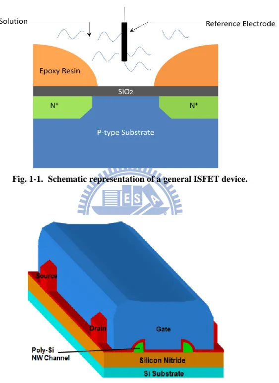
operates like an MOSFET but with its gate in the form of a reference electrode
inserted in a solution covering the gate oxide (SiO2), as shown in Fig. 1-1. The surface
of the gate oxide serves the role of the sensing site, on which the ions in the solution
5
higher sensitivity, other materials were explored and reported, like Al2O3 [31], Ta2O5
[32], Si3N4 [33], WO3 [34], SnO2 [35]. When the ions were bonded with the dielectric
surface, the surface potential of the material would be changed, so the channel
conductance of the FET device would vary accordingly. Generally, as more positive
ions are presented in an aqueous solution than the negative ones, they will induce
more native carriers (e.g., electrons) in the channel and hence increase the
conductance of an n-type FET device.
1-3
Motivation
In the past, the pH-meter was generally made of glass electrode, which would
make the equipment bulky and the users need to lug it to the places where
measurements are performed. In addition, glass is breakable and fragile so careful
handling adds to the cost. To solve these problems, some alternative structures have
been developed, like ISFET. As compared with former techniques, ISFET has many
advantages. First, it only needs a little media to expose. This favors the construction
of a small and portable test system. Second, its application is not restricted to pH
sensing but also some other fields of bio sensors. Third, since ISFET has a structure
6
cost [36, 37].
Although conventional ISFET has those advantages, it is not flawless. For
instance, in most cases it uses the planar device structure built on a bulk substrate, and
could suffer from the problems of subthreshold leakage currents, which will lead to a
higher S.S. and therefore a lower sensitivity. This phenomenon will be discussed in
this thesis later. To achieve high sensitivity and better response to the detection, in this
thesis we utilize a NW-FET to sense pH value. As mentioned above, due to the large
surface-to-volume ratio, NWFET possesses higher Ion / Ioff ratio and is sensitive to the
surface condition. Accordingly, we can utilize the output current difference to
differentiate the change of the pH value. Because it is fully compatible with silicon
processes with low-temperature thermal cycles during fabrication, the NW approaches
can be easily integrated with CMOS circuitry. To fabricate the device, tight control
over a number of structural parameters, such as the dimensions of the NW structures,
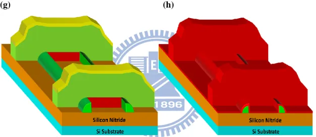
is needed. In this study we proposed and developed a novel method adopting sidewall
spacer method to form NWs TFT. The structure is shown in Fig.1-2 [38]. Such NW
sensors have been implemented with a micro-fluid scheme suitable for pH testing
7
1-4
Organizations of the Thesis
In this thesis, we will show the relationship between the different type of
structures, including planar and NW FETs, and the characteristics of pH
measurements. In this chapter we have already introduced NW technology and the
sensing structures. Then in Chapter 2, we will briefly describe the fabrications of “planar thick”, “planar thin” and “NW” structures. Besides, we will describe measurement methods, equipments and the relating theorem and characteristic in
detail with the device. In Chapter 3, we will describe sensing measurement
equipments and methods. Besides, the sensitivity and the characteristics of pH
measurement with respect to the different size of sensing area and structures will be
discussed. Finally, we will summarize the conclusion of this thesis and suggestions
8
Chapter 2
Device Structures, Fabrication and
Characteristic Analysis
As discussed in Chapter 1, in order to have high sensitivity, we have to reduce
the S.S.. To achieve this purpose, we have recently developed a method to fabricate
tiny NW as the channel of the devices [38]. The method is simple and low cost. To
illustrate the effectiveness of NW channel, in this thesis three structures were
fabricated and characterized. Two of them are with planar channel structures and the
last one is with NW channel structure. In each of the structures, two kinds of sensing
materials were employed, including aluminum oxide (Al2O3) and silicon oxide (SiO2).
In this chapter, we will describe the process flows of these devices and the
measurement settings
2-1
Process Flow and Structure of NW Devices
The top-view of the NW device is shown in Fig. 2-1(a). Fig. 2-1(b) is a
cross-sectional view of the device along Line aa’ in Fig. 2-1(a). A series of
9
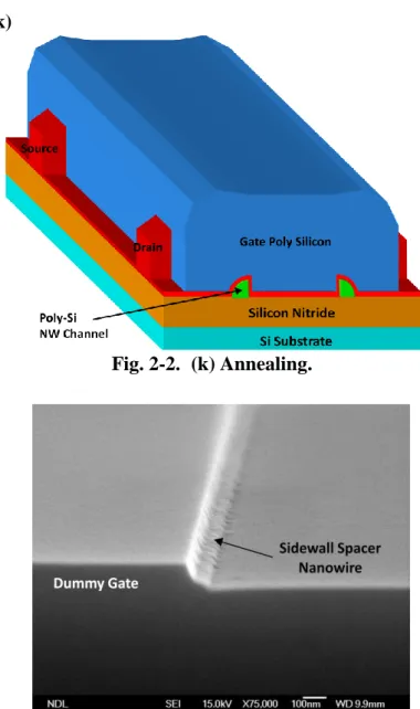
(k). All devices used in this work were fabricated on 6-inch silicon wafers. First, we
capped the wafers with 1500 Å silicon nitride (Si3N4) at 780 ℃ by the low pressure
chemical vapor deposition (LPCVD) system. Then, we deposited a layer of 1000 Å
TEOS oxide at 700 ℃ by LPCVD (Fig. 2-2(a)). Next, the oxide was patterned by
standard I-line lithographic and plasma etching steps (Fig. 2-2(b)) to form a dummy
structure. A 1000 Å -thick amorphous-silicon (α-Si) layer was then deposited at 560 ℃
by LPCVD (Fig. 2-2(c)). Next an annealing step was performed at 600 ℃ in N2
ambient for 24 hours to transform the α-Si into poly-Si (Fig. 2-2(d)). Afterwards, the
source/drain (S/D) implant was performed by P31+ implantation with dose of 5x1015 cm-2 and energy of 15 keV (Fig. 2-2(e)). An I-line lithographic step was then performed to generate S/D photoresist patterns, and the exposed poly-Si layer was
then etched by a reactive plasma etching step to define the S/D regions. During the
step, we could control the over-etching time to simultaneously form the poly-Si NW
spacers along the two sides of the dummy structure in a self-aligned manner with
respect to the S/D and gate (Fig. 2-2(f)). Note that, due to the low implantation energy,
the NW channels remained undoped after their formation. Figure 2-3 shows the SEM
image of the sidewall NW channels and the dummy structure. Diluted HF etching was
carried out in the subsequent step to remove the dummy structure (Fig. 2-2(g)). Next,
10
(Fig. 2-2(h)). Then, a 1000 Å -thick poly-Si was deposited at 620 ℃ by LPCVD to
serve as the top gate electrode (Fig. 2-2(i)). Afterwards, the top gate implant was
performed by P31+ implantation with a dose of 5x1015 cm-2 and energy of 35 keV (Fig. 2-2(j)). Next we used the I-line lithographic and stander plasma etching to define the
gate electrode. Then in order to reduce the S/D and gate resistance, the devices were
treated with a rapid thermal annealing (RTA) at 900 ℃ for 60 seconds (Fig. 2-2(k)).
The devices were then covered with an ONO stack consisting of 2000 Å -thick TEOS
oxide, 1000 Å -thick silicon nitride, and 1000 Å -thick TEOS oxide, all deposited by
LPCVD. The inserted nitride was used to enhance the water-repellent property of the
devices during sensing test. After the formation of contact holes, we split the wafer
into two groups with different pad materials filling in the contact holes, namely,
aluminum, and in-situ doped n+ poly-Si. These materials were subsequently defined to serve as the test pads for device characterization. Finally, all devices received a
forming gas sintering step at 400 ℃ for 30 minutes. Figure 2-4 shows the
cross-sectional SEM image of the NW structure. From this image, we can observe
that the channel height and thickness are approximately 40 nm and 50 nm,
11
2-2
Process Flow and Structure of Planar
Devices
For comparison with the NW structures, we’ve also fabricated the planar devices
with various channel thickness.
2-2-1 Planar Device with Thin Channel
The top view of the “planar-thin” devices is also shown in Fig. 2-1(a). The
cross-section views formed after different steps of fabrication along Line bb’ in Fig.
2.1(a) are shown in Figs. 2-5(a) to (i). First, the 6-inch wafers were capped with a
1500 Å silicon nitride and a 500 Å in-situ doped n+ poly-Si (Fig. 2-5(a)). After standard I-line lithography and plasma etching to define the S/D regions (Fig. 2-5(b)),
we deposited a 100 Å -thick amorphous silicon layer (Fig. 2-5(c)). Then, an annealing
step was performed at 600 ℃ in N2 ambient for 24 hours to transform the α-Si into
poly-Si (Fig. 2-5(d)). The channel was then defined by another I-line and plasma
etching steps (Fig. 2-5(e)). Note that the S/D thickness is much thicker than the
channel in order to reduce the parasitic resistance. Next, a 300 Å -thick TEOS was
deposited to serve as the gate oxide (Fig. 2-5(f)), then a 1000 Å -thick gate poly-Si
12
performed by P31+ implantation with dose of 5x1015 cm-2 and energy of 35 keV (Fig. 2-5(h)). After the gate formation, an RTA annealing with 900 ℃ for 30 seconds was
performed to reduce S/D and gate resistance (Fig. 2-5(i)). The subsequent fabrication
flow was the same as that used in NW device fabrication.
2-2-2 Planar Device with Thick Channel
The top view of this structure is the same as that shown in Fig. 2-1(a). The
fabrication steps with the cross-section views along Line bb’ in Fig. 2-1(a) are
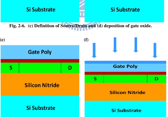
shown in Figs. 2-6(a) to (i). To begin with, a 1500 Å -thick silicon nitride layer was
first capped on Si wafer surface, followed by the deposition of an α-Si layer of 500 Å
(Fig. 2-6(a)). After the annealing step performing at 600 ℃ in N2 ambient for 24 hours
to transform α-Si into poly-Si (Fig. 2-6(b)), the active region is formed (Fig. 2-6(c)). Then, we deposited a 300 Å -thick TEOS oxide as the gate oxide (Fig. 2-6(d)), and a
1000 Å -thick poly-Si layer as the gate material (Fig. 2-6(e)). Afterwards, the top gate
implant was performed by P31+ implantation with dose of 5x1015 cm-2 and energy of 35 keV (Fig. 2-6(f)). In the subsequent step, we used I-line photolithographic and
plasma etching steps to define the gate region (Fig. 2-6(g)), then performing a P31+ implant with dose of 5x1015 cm-2 and energy of 35 keV to dope the S/D and gate (Fig
13
2-6(h)). Dopant activation was done by performing RTA at 900 ℃ for 30 seconds (Fig.
2-6(i)). The subsequent processes were the same as that used in fabricating devices
with thin channel.
2-3
Measurement Setups and Electrical
Characteristics of the Fabricated Devices
2-3-1 Measurement System
All electrical characteristics of the devices characterized in this thesis were
measured by an automated system consisting of switching system-708A, Model 4200
Semiconductor Characterization System (Model 4200-SCS) with built-in software,
and Keithley Interactive Test Environment (KITE).
2-3-2 Theory and Model of Threshold Voltage
Variation
Because of the device scaling, the dopant counts in channel region of modern
nano-scale CMOS devices may fall less than a few hundreds. In this situation, random
dopant distribution in depletion region is one of the possible reasons to induce Vt
14 DEP t FB S OX Q V V C , (2-1) where VFB is the flat band voltage, Sis the surface potential between oxide and
channel, QDEP is the charge within the depletion region, and COX is the capacitance of
gate oxide per unit area. From the formula, we can see that the last term is related to
the dopant distribution, so it represents an impact factor to affect the Vt . According to
Takeuchi’s model [40], Vt shift ( ΔVt ) can be described as
0 1 DEP t OX DEP x Q V C W (2-2) In order to simplify the model, he assumed that all the parameters are constant, except
the dopant distribution. This formula is based on scheme shown in the Fig. 2-7(a)
which assumes that additional charges (ΔQDEP) at the position (x0) along X-axis
within maximum depletion width (WDEP) will cause the surface potential and Vt shifts.
The solid line in Fig. 2-7(b) represents the original electric field distribution in the
depletion region induced by substrate doping (NSUB) without any additional charge
and the surface electrical field is E0. When ΔQDEP is added, there will be a potential
drop at x0. In order to balance this phenomenon, the surface electric field will be
enhanced by ΔE, and the electric field distribution is modified as shown by the dashed
line. Such modification affects the surface potential and makes Vt change.
15 Poisson’s statistics [41], so
SUB DEP q N x L W x Q L W , (2-3) where W is the channel width and L is the channel length. By substituting Eq. (2-3)into Eq. (2-2), and integrating all the contribution of ΔQDEP in the depletion region
from x = 0 to x = WDEP, we obtain
3 EFF DEP t OX N W q V C L W , (2-4) where NEFF is a weighted average of NSUB(x) defined as
0 2 3 WDEP ( ) (1 ) EFF SUB DEP DEP x dx N N x W W
. (2-5)We can see in Eq. (2-4) that ΔVt is inversely proportional to the L and W which are
related to the dimensions of the devices, and proportional to the WDEP which is related
to the channel thickness for devices with a fully-depleted channel.
In this study, no intentional channel doping was performed in the poly-Si
channel. Nevertheless, the trapping sites located in or near the grain boundaries may
play a similar role to that of random dopants in the bulk CMOS devices. This is
because their charge state is affected by the gate bias and may affect Vt. This means
we can adopt the above theory and replace the parameter NSUB with NTRAP to analyze
16
effect and the deviation of the Vt will be discussed in the end of this section.
2-3-3 Comparisons of Basic Electrical Characteristics
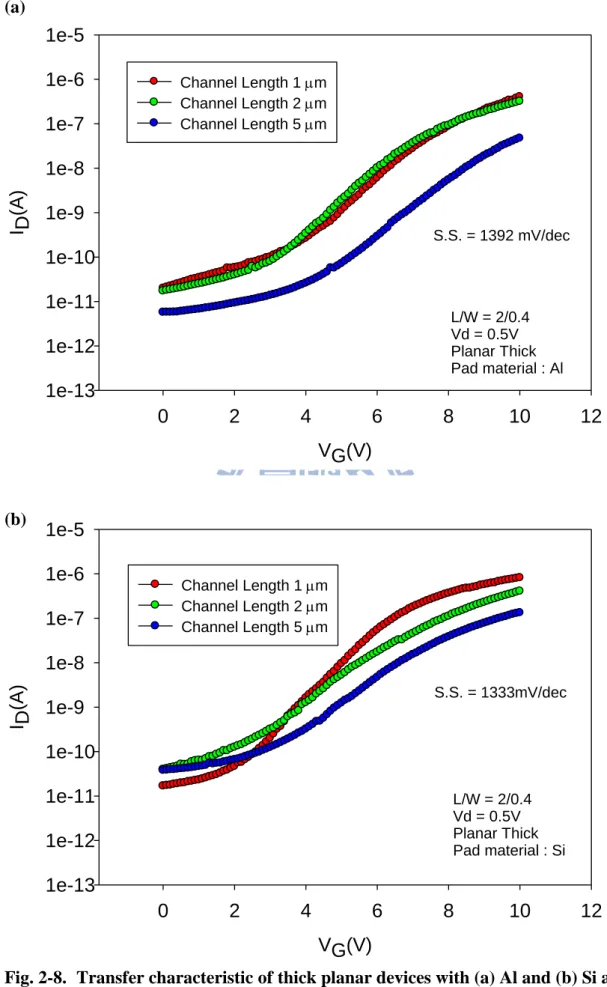
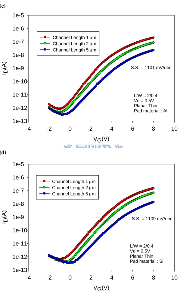
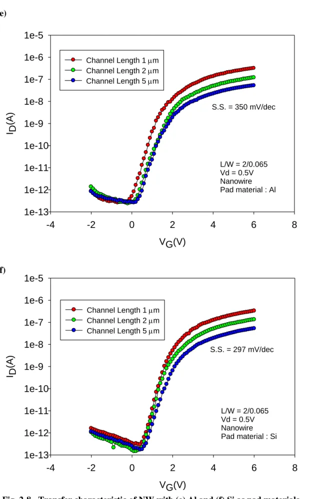
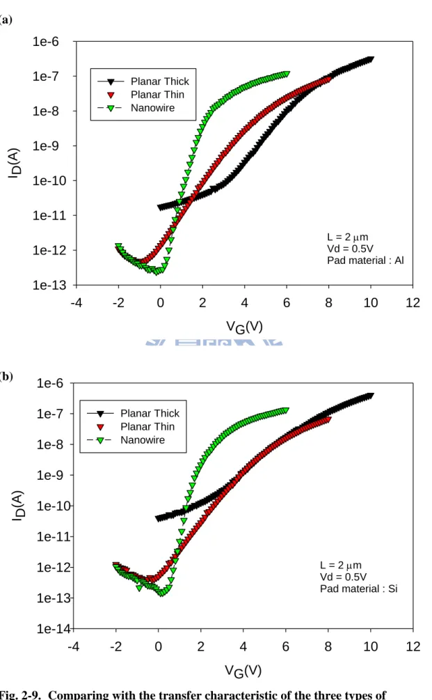
Figs. 2-8(a) to (f) show typical ID-VG curves of the three types of structures and
two different pad materials. From the curves, we can see the slopes of the “planar-thick” device in the linear region are the smallest, and those of the NW’s are the largest. It means that if we use NW, the largest current difference can be obtained
in a small change in VG. This is one of the reasons why we want to use the NW
structures for sensor applications. To compare the characteristics more clearly, we
utilize the S.S. that is defined as below:
1 log . . D G I S S V (mV/dec). (2-6)We can find that the mean S.S. of the NW is much smaller than that of the planar ones.
It is because NW channel has the largest surface-to-volume ratio, and the gate is more
effective in control the turning on and off of the channel. Besides, the off-state
leakage is dramatically reduced with ultra-thin channel thickness, as compared with
the planar device with thick channel.
17
largest (~106) among the devices, while the planar devices with thick channel is the worst. This is because of the off leakage currents of the thick planar devices which is
much larger than the other two structures as mentioned above. The gate is difficult to
control the deeper portion of channel which is responsible for the off-state leakage.
Figs. 2-9(a) and (b) show the ID-VG curves of different structures and pad materials.
We can clearly see that the NW structure has the best performance among the test
devices.
We also compare the mobility performance of the devices by measuring the
field-effect mobility which is defined as,
field-effect mobility ( FE) m D OX L G W C V (cm2/V-s), (2-7)
where Cox is the gate oxide capacitance per unit area, W is the channel width, and Gm
stands for the transconductance given by,
.
|
D D m G V const I G V .(2-8)
Figs. 2-10(a) and (b) present the mobility of the three types of devices with various
pad materials. We can see that the mobility of the NW and thick planar devices are
larger than that of the thin planar ones. One of the possible reasons is the small grains
size contained in the ultra-thin (~ 100 Å ) channel of the thin planar devices. In this
18
would be limited by the heterogeneous nucleation process at the interfaces and the
grain size thus shrunk Figs. 2-11(a) and (b) are the schematic drawings to explain the
phenomenon. For the case when the channel thickness is thin, as shown in Fig.
2-11(a), the grains size will be limited by the thickness, so mobility and the
conduction current will suffer from more scattering with the grains boundaries than
the case with a thick channel. Besides, although the original α-Si film thickness of
NW devices (1000 Å ) is two times larger than that of the planar thick (500 Å ), the
mobility is not much bigger. This is attributed to the fact that the portion of the final
NW channel is near the side wall of the dummy structure, and generally the grains
size near the interface is smaller than the outer part, thus the benefit of an increased
grain size with increasing thickness is not significant. Figs. 2-12(a) and (b) are the
variation of the mobility. We can see the mean value of the mobility is the best for
NW even though the channel thickness is the smallest.
Next, we compare the deviation of threshold voltage among the different
structures. Figures 2-13(a) to (f) are the ID-VG curves of fifteen devices measured
from the three types of structures with various pad materials. The channel length of
the devices was 2 µm, the channel width is 0.4 µm for planar and 65 nm for NW, and
the channel thickness is 500, 100 and 400 Å for “planar-thick”, “planar-thin” and “NW”, respectively. First, from the diagrams, we can clearly see that the variation is
19
the worst for the thick planar devices, while the NW devices are the best. Figs. 2-14(a)
to (c) and Figs. 2-15(a) to (c) are the mean Vt from different structures and pad
materials with channel length of 1µm, 2µm and 5µm, respectively. Vt is defined as VG
at ID = W/L × 10 nA. The error bar in the figures represents the standard deviation in
Vt. We can find the deviation shows the identical trend. That is, when the channel
length increases, the deviation decreases. As mentioned before, discrete random
dopant (or trap) in the depletion region of the channel plays a main role in affecting
the threshold voltage deviation. Then, according to Eq. 2-4, the ΔVt will be
proportional to WDEP, and inversely proportional to L and W. It seems that this
phenomenon that we discovered can be well explained by the effect. In order to verify
this assumption, we plot ΔVt versus 1 / LW in Fig. 2-16. It means that the ΔVt for
this effect will be only affected by WDEP, and proportional to it. First, we compare the
thick and thin planar devices. Since the channel thickness of the fabricated devices is
pretty thin (only 500 Å even for the “thick” planar split), WDEP is assumed to be the
channel thickness. Because the thickness of thick planar devices is thicker than the
thin planar ones, we can see the ΔVt of planar thick is bigger. It means that there are
more ΔQDEP as the channel becomes thicker, so the ΔVt is larger. On the other hand,
the channel in NW is of triangular column, so we can’t directly use the channel
20
the average WDEP:
(average)
( ) ( )
DEP TRAP DEP TRAP CHANNEL TRAP DEP COVERED
Q qN W L W qN V qN W W L ,(2-9)
where VCHANNEL is volume of the channel, WDEP(average) is the average depletion width
and WCOVERED is the gated channel width. Because it is fully depleted, the last term of
the original formula can be represented by the volume of the channel. Then, we can
utilize the channel surface area that is covered by gate to calculate the average WDEP.
And we can find that the WDEP of NW is around 80 Å which is smaller than the thin
planar ones, so we can get the smallest slope for NW in Fig. 2-16. In other words, NW
has the best control over the threshold voltage variation.
We also compare the ΔS.S. among the different structures. Figures 2-17(a) and (b)
show the mean value of S.S. and ΔS.S. of the test samples. The channel length of all
samples is 2 µm. Again it can be seen that the thick planar device has the largest ΔS.S.,
and NW has the smallest deviation. As mentioned before, NW has the largest surface
to volume ratio, which can increase gate coverage within finite channel region. The
smallest mean value and standard deviation of S.S. with the NW split reflect this trend.
21
Chapter 3
Analysis of the Characteristics of pH Sensors
3-1
Microfluidics Settings and Measurement
Methods
The electrical measurement equipment for pH sensors is the same as that
mentioned in Sec. 2-3. The microfluidic channel system which houses the test devices
is composed of a base (Fig. 3-1), a microfluidic channel made of
polydimethylsiloxane (PDMS) (Fig. 3-2), and a plastic mold used to press the PDMS
(Fig. 3-3). Construction of these components is shown in Fig. 3-4, and the final views
are shown in Figs. 3-5(a) and (b). The chemical constitution of PDMS is shown in Fig.
3-6. Normally we can clean the material using acetone only. Major advantages of the
PDMS approach are summarized in Table 3-1. For those merits, it becomes one of the
most attractive materials for microfluidic device.
All the pH solutions were deployed by using phosphate buffered saline
(PBS)(10mM, pH7.4, 13mM Na2HPO4, 2.26mM KH2PO4). NaOH was used to make
it more basic, while H3PO4 was used for opposite purpose. The glass electrode pH
22
intended to test. The reference electrode material was silver. Figure 3-7 is the
schematic illustration of the test configuration equipped with the poly-Si NW devices.
When starting experimental measurements, we injected the test solution into the
microfluidic system via an inlet tube (see Fig. 3-3). The solution was then flowed
through the microfluidic channel of the PDMS microfluidics where the sensing pad of
the test device was located, and was then flowed out via the outlet tube (see Fig. 3-3).
To make the flow stable, a string pump (Fig. 3-8) was used for automatic injection.
During the measurement solutions with various pH values were injected sequentially
and we could measure the real-time drain current characteristics (i.e., Id vs. time) at a
fixed VG condition operated in subthreshold region. The set VG was determined in the
beginning of the test by first measuring the ID-VG curve. Throughout the test Vd was
set at 0.5 V. For real-time characterization, evolution of drain current measured under
the appropriate VG with the flowing solution of varying pH values was recorded.
However, as the pH of the test solution was changed to a new value, it needed a
period of time to become stable. A typical example is given in Fig. 3-9. As can be
seen in the figure, as the pH is varied from 9 to 10, a drop in drain current occurs and
takes several hundreds of seconds to reach the steady state. The difference between
the new stable Id and the previous stable one is then recorded and used as an indicator
23
In addition, we can also derive the shift in Vt from the drain current difference. Figure
3-10 shows the subthreshold characteristics of a test device measured in solutions
with pH ranging from 7 to 10. It can be seen that a change in pH results in a parallel
shift in the I-V curves and thus S.S. remains the same. From this we can, based on the
relation shown in Fig. 3-11, derive the shift in Vt from the drain current difference.
Based on the scheme, Vt shift is used as another indicator for analyzing the sensitivity
of the testers.
3-2
The Theory of pH Sensors
Variation in pH value of the test solutions is responsible for the variation of
sensing signal. According to its definition, pH can be expressed as
log[ ]b
pH H , (3-1) where [H+]b is the bulk concentration of H+ ions in the solution. It implies that sensors
can detect the change of pH because of the variation in the concentration of H+ ions. The most plausible reason to explain why sensors can detect the variation of
[H+]b is based on the site-binding model. The model was first introduced in 1974 by
Yates et al. [42] to describe the properties of an oxide/aqueous electrolyte interface. In
24
OH, and A − OH2+, as shown in Fig. 3-12. The neutral A − OH sites are characterized
by the equilibrium constants Ka and Kb, and can be written as the following equations,
, (3-2) , (3-3) , (3-4)
, (3-5) where A − O−, A − OH, and A − OH2+ are the negative, neutral and positive surface
sites, respectively, Ka and Kb are the equilibrium constants, and [A − O−], [A − OH]
and [A − OH2+] are the numbers of the surface sites per unit area. Note that [H+]S is
the concentration of the H+ ions in solution near the surface, and the relationship between [H+]S and the bulk concentration [H+]b can be written by the Boltzmann
equation,
, (3-6)
where is the pH-dependent surface potential, K is the Boltzmann constant, q is
the elementary charge, and T is the absolute temperature. The surface potential is
actually correlated with the net surface charge density,
. (3-7) According to Eq. 3-2 and 3-3, for instance, if σ 0 at pH 7 is zero, we know that
for an acid, the predominant concentration of H+ ions will cause the reaction to a K A OH A OH 2 b K A OH H A OH [ ][ ] [ ] S a A O H K A OH 2 [ ] [ ][ ] b S A OH K A OH H 0 [H ]S [H ] exp(b q ) KT 0 0 ([A OH2 ] [A O ])
25
generate A − OH2+. In other words, [A − OH2+] is more than [A − O−], so by Eq. 3-7
the surface potential will be positive. Conversely it is negative in a basic solution.
Because of the change of surface potential with varied pH value of the test solution,
we can see the change of electrical characteristics.
In this study, we employed two types of sensing pad materials, namely, Al and Si.
Naturally, the surface of the materials forms a native oxide layer which becomes
practical sensing site of the sensing antenna connected to the sensor devices. Through
the conductive solution, we can apply a voltage to the antenna pad through a probe
immersing inside the test solution without practically contacting the electrode. Owing
to the change of surface potential caused by the reactions mentioned above, the
effective gate voltage will be enhanced or decreased. This change reflects on a
modification of the output currents (ID) which is recorded and analyzed.
3-3
Analysis of pH Sensing Characteristics
3-3-1 The Sensitivity of Different Structures
In this experiment, the test solution starts at pH 3 and then pH 3-5-7-9 in
26
“reduced current response ratio”, as follows:
, (3-8)
where ID3 is the drain currents at pH 3 (i.e., the initial drain current), and IDX is the
drain currents at pH X (X = 3, 5, 7, 9). Fig. 3-13 shows the reduced current response
ratio as a function of the pH value for NW and planar devices having a SiO2 sensing
layer. In this plot the antenna area is 30x60 μm2
. We can observe that, among the test
devices, the NW structure has the strongest response for the variation of pH, and the
planar device with thick channel is the worst. With the fitting lines included in the
figure, we can see the reduced current response sensitivity of NW devices is 2.5 times
higher than that of the thick planar device. This is because the NW sample has the
best S.S. as have been shown in Section 2-3. This means that a small change in
surface potential of the sensing pad will cause a larger change of drain currents or, in
other words, a greater response. This demonstrates the effectiveness of utilizing the
NW structures as a sensor. Figure 3-14 shows the Vt shift derived from the results
shown in Fig. 3-13. Again, the NW device exhibits better sensitivity than the planar
counterparts. Figures 3-15 (a) ~ (c) show the real-time drain current measurements of
the test devices.
3 3
Reduced current response ratio = D DX 100%
D I I
I
27
3-3-2 Effects of Antenna Pad Area
Here we will discuss the relationship between the exposed area of sensing layer
and pH sensitivity. In a set of experiments, the testing starts by placing the test device
in the test solution with pH 3, followed by injecting various test solutions with a pH
sequence of 3-5-7-9. Here we use the Vt at pH 3 as the reference voltage to calculate
and get the shift in Vt at each stage with respective to that with pH 3. Figure 3-16
shows the enhanced Vt response for three NW devices with various sensing (antenna)
areas as a function of pH, and the material of the sensing layer is SiO2. We can find an
increase in antenna area tends to increase the sensitivity. In the figure, the sensitivities
are 57.1, 50.8, and 45.2mV/pH for pad area of 200x500, 100x100, and 30x60 μm2, respectively. According to Eq. 3-7, we know that the surface potential is decided by
the number of A-OH2+ and A-O −
sites. The above trend can thus be attributed to the
fact that a larger pad can provide more binding sites and therefore renders a bigger
change in the amount of charges bonded to the sensing pad as the pH of the test
solutions is varied. Figure 3-17 is the reduced current response ratio as a function of
pH for the three devices. This is due to the fact that, in this indicator, the current has
been normalized to the initial current level. However, as it is transformed into the Vt,
28
Figures 3-18(a) to (c) show the real-time drain current measurements performed on
the devices.
3-3-3 Effects of Antenna Pad Materials
Figure 3-19 shows the sensitivity of NW devices with Al2O3 sensing pad of
different sensing pad area. In the measurements, the pH value of the test solution
started at 7, and with a sequence of 7-8-9-10. Here we used the Vt at pH 7 as the
reference voltage, and then calculated and obtained the shift in Vt as the pH of the test
solution is changed. In this figure we can find the sensitivity of devices with Al2O3 as
the sensing material still shows a positive correlation with antenna pad area. Besides,
from Figs. 3-20(a) to (d), we can easily see the value of the Vt shift becomes apparent
when the antenna pad is larger. Figure 3-21 is a figure showing the current response
ratio for these devices at different pH. We can discover the current response of Al2O3
surpasses that of SiO2 shown in Fig. 3-17. This in turn results in the greatly enhanced
sensitivity of devices with Al2O3 sensing pad shown in Fig. 3-19 over that with SiO2
shown in Fig. 3-16. One interesting finding shown in Fig. 3-19 is the extremely high
sensitivity (> 120 mV/pH) exhibited by the NW devices with Al2O3 sensing material.
29
temperature proposed by P. Bergveld [43]. Figures 3-22(a) to (d) are the results of
real-time measurements performed on these devices. Although such high sensitivity is
intriguing and could be of importance for practical application, origins for the
phenomenon are still unknown and need additional efforts to investigate and disclose.
Other test procedures are shown in Figs. 3-23 (a) and (b), respectively, for
probing the hysteresis characteristics of the tester with an Al2O3 sensing pad in a loop
time of 1260 s. The real-time diagrams obtained from the tests are shown in Figs.
3-24(a) and (b). The shift in Vt in each stage during testing with respect to the Vt at pH
7 at time zero for the acid- and basic- cycles are shown in Figs.3-25 (a) and (b),
respectively. In these figures it can be seen that the two datum points recorded at pH 7
do not coincide actually, indicating the occurrence of hysteresis. We can see the
difference of point a and b is 10.9 mV, which is smaller than the difference (22.2 mV)
of point b’ and c’. This means the hysteresis in acid is smaller than that in basic
solutions. There are two possible reasons to explain this phenomenon. The first one
was brought up by L. Bousse et al [45]. The explanation is that the dominant ion
species H+ in acid solutions is smaller and lighter than the OH- ions in basic solutions, so it is easier and faster for H+ to go through the sensing material. It can thus reduce the total reaction time. So we will find the hysteresis in acid is smaller in basic
30
exhibiting in basic solutions than acid ones. So in limited time period, it is more
31
Chapter 4
Conclusion and Future Work
4-1
Conclusion
In this thesis, we have developed a simple method to fabricate poly-Si NWTFTs.
In the device fabrication sidewall spacer etching technique was used to define the NW
patterns, and no advanced or expensive lithographical tools like e-beam writer was
involved. We’ve also utilized the fabricated NWTFTs as a test vehicle for sensing pH
of chemical solutions. In this scheme, the NW channel was connected to an antenna
test pad with varied area and pad material. For comparison purpose, planar devices
were also fabricated and compared. Among the test devices, NW structures exhibit the
best performance in terms of lowest leakage current, smallest S.S. and highest on/off
currents ratio, owing to the high surface-to-volume ratio and tiny channel dimensions.
For device variation issue, the standard deviation of Vt is shown to be inversely
proportioned to WL and proportional to the depletion width. Because of the
superior gate controllability, NW devices also present the tightest control over Vt and
S.S. variations.
32
see that the NW structures have the best sensitivity as compared with planar devices.
In addition, the results show that the relationship between sensitivity and the sensing
pad area is positive. Regarding the sensing pad materials, our results indicate that
Al2O3 has better sensitivity than SiO2. Moreover, the sensitivity of the test devices
with Al2O3 sensing pad can be much larger than the limitation of 60 mV/pH at room
temperature, predicted in previous theory [43], although details about origins of this
phenomenon remain unclear. We’ve also measured the hysteresis characteristics of pH
testing. The results indicate the hysteresis in acid is smaller than that in basic. This is
attributed to the smaller size and lighter mass of H+, the major reactants in acid, over that of OH- in basic solution. As a result, H+ ions move more quickly and reduce the response time within reaction. Therefore, the hysteresis in acid is smaller than that in
basic.
4-2
Future Work
In this thesis, we found the sensitivity transcended the theoretical limit value
(60mV/pH) at room temperature when using Al2O3 as the antenna pad material.
Nevertheless, such phenomenon was not seen as SiO2 was used as the sensing material.
Certainly it needs more efforts to clarify the associated mechanisms. Examination of
33
The environmental noise is always an annoying factor in experiments. In order to
improve the quality of experiments, the construction of an advanced testing
environment and equipment with high precision and automatic measurement
34
References
[1] J. Hu, T. W. Odom, and C. M. Lieber, “Chemistry and physics in one dimension: synthesis and properties of nanowires and nanotubes,” Acc. Chem.
Res., pp. 435-455, 1999.
[2] H. C. Lin and S. M. Sze, “Nanoelectronic technology: in search of the ultimate device structure,” Future trends in microelectronics: the nano millennium, S. Luryi, J. M. Xu, and A. Zaslavsky, eds., pp. 4-14 (New York: Wiley 2004).
[3] L. Chang, Y. K. Choi, D. Ha, P. Ranade, S. Xiong, J. Bokor, C. Hu, and T. J. King, “Extremely scaled silicon nano-CMOS devices,” Proceedings of the IEEE, vol. 91, no. 11, pp. 1860-1873, Nov. 2003.
[4] B. Doyle, S. Hareland, B. Jin, J. Kavalieros, T. Linton, R. Rios, and R. Chau, “Tri-gate fully-depleted CMOS transistors: fabrication, design and layout,”
VLSI Symp. Tech. Dig., pp. 10-12, June 2003.
[5] X. Duan, C. Niu, V. Sahi, J. Chen, J. W. Parce, S. Empedocles, and J. L. Goldman, “High-performance thin-film transistors using semiconductor nanowires and nanoribbons,” Nature, vol. 425, pp. 274-278, 2003.
[6] X. Duan, Y. Huang, and C. M. Lieber, “Nonvolatile memory and programmable logic from molecule-gated nanowires,” Nano Lett., vol. 2,
35
no. 5, pp. 487-490, 2002.
[7] M. Specht, R. Kommling, L. Dreeskornfeld, W. Weher, F. Hofmann, D. Alvarez,
J. Kretz, R. J. Luyken, W. Rosner, H. Reisinger, E. Landgraf, T. Schulz, J.
Hartwich, M. Stadele,V. Klandievski, E. Hartmann, and L. Risch, “Sub-40nm
tri-gate charge trapping nonvolatile memory cells for high -density applications,” VLSI Symp. Tech. Dig., pp. 244-245, 2004.
[8] M. C. McAlpine, R. S. Friedman, S. Jin, K. H. Lin, W. U. Wang and C. M. Lieber, “High-performance nanowire electronics and photonics on glass and plastic substrates,” Nano Lett., vol. 3, pp. 1531-1535, 2003.
[9] Y. Cui, Q. Wei, H. Park, and C. M. Lieber, “Nanowire nanosensors for highly sensitive and selective detection of biological and chemical species,” Science, vol. 293, pp. 1289-1292, 2001.
[10] Z. Li, Y. Chen, X. Li, T. I. Kamins, K. Nauka, and R. S. Williams, “Sequence-specific label-free DNA sensors based on silicon nanowires,” Nano
Latt., vol. 4, pp. 245-247, 2004.
[11] A. M. Morales and C. M. Lieber, “A laser ablation method for the synthesis of crystalline semiconductor nanowires,” Science, vol. 279, no. 5348, pp. 208-211, 1998.
36
Krishnamohan, and K. C. Saraswat, “Germanium nanowire field-effect
transistors with SiO2 and high-κ HfO2 gate dielectrics,” Appl. Phys. Lett.,
vol. 83, no. 12, pp. 2432-2434, 2003.
[13] H. F. Yan, Y. J. Xing, Q. L. Hang, D. P. Yu, Y. P. Wang, J. Xu, Z. H. Xi, and S.
Q. Feng, “Growth of amorphous silicon nanowires via a solid–liquid–solid mechanism,” Chemical Physics Lett., vol. 323, no. 3-4, pp. 224-228, June 2000.
[14] N. Wang, Y. F. Zhang, Y. H. Tang, C. S. Lee, and S. T. Lee, “SiO2-enhanced
synthesis of Si nanowires by laser ablation,” Appl. Phys. Lett., vol. 73, no. 26, pp. 3902-3904, 1998.
[15] Y. Huang, X. Duan, Q. Wei, and C. M. Lieber, “Directed assembly of
one-dimensional nanostructures into functional networks,” Science, vol. 291, pp.
630-633, 2001.
[16] X. Duan, Y. Huang, Y. Cui, J. Wang, and C. M. Lieber, “Indium phosphide
nanowires as building blocks for nanoscale electronic and optoelectronic devices,” Nature, vol. 409, pp. 66-69, 2001.
[17] A. Tao, F. Kim, C. Hess, J. Goldberger, R. He, Y. Sun, Y. Xia, and P. Yang, “Langmuir-Blodgett silver nanowire monolayers for molecular sensing using surface-enhanced Raman spectroscopy,” Nano Lett., vol. 3, pp. 1229-1233,
37
2003.
[18] H. C. Lin, M. F. Wang, F. J. Hou, H. N. Lin, C. Y. Lu, J. T. Liu, and T. Y. Huang, “High-performance p-channel schottky-barrier SOI FinFET featuring self-aligned PtSi source/drain and electrical junctions,” IEEE Electron Device
Lett., vol. 24, no. 2, pp. 102-104, 2003.
[19] F. L. Yang, D. H. Lee, H. Y. Chen, C. Y. Chang, S. D. Liu, and C. C. Huang et
al, “5 nm-gate nanowire FinFET,” VLSI Symp. Tech. Dig., pp. 196-197, June
2004.
[20] M. D. Austin, H. Ge, W. Wu, M. Li, Z. Yu, D. Wasserman, S. A. Lyon, and S. Y.
Chou, “Fabrication of 5 nm line-width and 14nm pitch features by nanoimprint lithography,” Appl. Phys. Lett., vol. 84, pp. 2599-2601, 2004.
[21] J. Gu, C. P. Jen, Q. Wei, C. Chou, and F. Zenhausern, “Mask fabrication
towards sub-10 nm imprint lithography,” Proc. SPIE, vol. 5751, pp. 382-391,
2005.
[22] M. D. Austin and S. Y. Chou, “Fabrication of 70 nm channel length polymer
organic thin-film transistors using nanoimprint lithography,” Appl. Phys.
Lett., vol. 81, no. 23, pp. 4431-4433, 2002.
[23] Y. K. Choi, Ji. Zhu, J. Grunes, J. Bokor, and G. A. Somorjai, “Fabrication of
38 . B, vol. 107, no. 15, pp. 3340-3343, 2003.
[24] H. L. Chen, C. H. Chen, and F. H. Ko, “Thermal-flow techniques for sub-35
nm contact-hole fabrication in electron-beam lithography,” J. Vac. Sci. Technol.
B, vol. 20, no. 6, pp. 2973-2978, 2002.
[25] F. H. Ko, H. C. You, T. C. Chu, T. F. Lei, C. C. Hsu, and H. L. Chen, “Fabrication of sub-60-nm contact holes in silicon dioxide layers,”
Microelectronic Engineering, vol. 73-74, pp. 323-329, 2004.
[26] I. Lundstrom, S. Shivaraman, C. Svenson, and L. Lundkvist, ”A
hydrogen–sensitive MOS field–effect transistor,” Appl Phys Lett., vol. 26, no. 2, pp. 55-57, 1975.
[27] L. S. Jung, C. T. Campbell, T. M. Chinowsky, M. N. Mar, and S. S. Yee, “Quantitative interpretation of the response of surface plasmon resonance sensors to adsorbed films,” Langmuir, vol. 14, no. 19, pp. 5636-5648, 1998.
[28] Z. Davis, G. Abadal, O. Kuhn, O. Hansen, F. Grey, and A. Boisen, "Fabrication
and characterization of nano-resonating devices for mass detection, " J. Vac. Sci.
Technol. B, vol. 18, no. 2, pp. 612-616, 2000.
[29] Y. L. Chin, J. C. Chou, T. P. Sun, W. Y. Chung, and S. K. Hsiung, “A novel pH
39
process,” Sensors and Actuators B, vol. 76, no. 1-3, pp. 582-593, June 2001 . [30] P. Bergveld, “Development of an ion sensitive solid -state device for
neurophysiological measurements,” IEEE Trans. Biomed. Eng., vol. 17, pp. 70-71, 1970.
[31] J. C. Chou, “Study on the temperature effects of Al2O3 gate pH-ISFET,”
Material Chemistry and Physics, vol. 81, no. 2-3, pp. 152-157, January
2002.
[32] Y. Ito, “Long-term drift mechanism of Ta2O5 gate pH-ISFETs,” Sensors
and Actuators B, vol. 64, no. 1-3, pp. 152-155, June 2000.
[33] G. T. Yu, “Hydrogen ion diffusion coefficient of silicon nitride thin films,”
Applied Surface Science, vol. 202, no. 1-2, pp. 68-72, December 2002.
[34] J. C. Chou, “Ion sensitive field effect transistor with amorphous tungsten trioxide gate for pH sensing,” Sensors and Actuators B, vol. 62, no. 2, pp. 81-87, February 2000.
[35] H. K. Liao, “Study of amorphous tin oxide thin films for ISFET applications,” Sensors and Actuators B, vol. 50, no. 2, pp. 104-109, July 1998.
[36] A. Merlos, E. Cabruja, and J. Esteve, “New technology for easy and fully
40
B, vol. 24, no. 1-3, pp. 228-231, March 1995.
[37] E. Lauwers, “A CMOS multiparameter biochemical microsensor with temperature control and signal interfacing,” IEEE Journal of solid state circuit vol. 36, no. 12, pp. 2030-2038, December 2001.
[38] H. C. Lin, M. H. Lee, C. J. Su, T. Y. Huang, C. C. Lee, and Y. S. Yang, “A
simple and low-cost method to fabricate TFTs with poly-Si nanowire
channel,” IEEE Electron Device Letters, vol. 26, no. 9, pp. 643-645, September
2005.
[39] K. Nishinohara, N. Shigyo, and T. Wada, “Effects of microscopic fluctuations in
dopant distributions on MOSFET threshold voltage,” IEEE Transactionss on
Electron Devices, vol. 39, no. 3, pp. 634-369, 1992.
[40] K. Takeuchi, T. Tatsumi, and A. Furukawa, “Channel engineering
for t he reduct i on of random -dopant -pl acem ent -i nduced t hres hol d voltage fluctuation,” Integrated Event Delivery Management (IEDM), pp.841-844, 1997.
[41] N. Sano, K. Matsuzawa, A. Hiroki, and N. Nakayama, “Probability distribution
of t h r e s h ol d v ol t a g e fl u ct u a t i o ns i n m et al ox i d e s em i c on du ct or
f i e l d - e f f e c t - t r a n s i s t o r s , ” J a p a n e s e J o u r n a l o f A p p l i e d P h y s i c s ,