國立交通大學
電子工程系 電子研究所碩士班
碩士論文
利用雙重微影成像法製作非對稱 P 型金
氧半場效電晶體之研究
Fabrication of Asymmetric PMOSFETs
with Double-Patterning Technique
研究生 :張格綸
指導教授 :林鴻志 博士
黃調元 博士
利用雙重微影成像法製作非對稱 P 型金氧半場
效電晶體之研究
Fabrication of Asymmetric PMOSFETs with
Double-Patterning Technique
研究生:張格綸
指導教授:林鴻志 博士
黃調元 博士
Student: Ke-Lun Chang
Advisors: Dr. Horng-Chih Lin
Dr. Tiao-Yuan Huang
國立交通大學
電子工程系 電子研究所碩士班
碩士論文
A Thesis
Submitted to Department of Electronics Engineering and Institute of Electronics College of Electrical and Computer Engineering
National Chiao-Tung University
in Partial Fulfillment of the Requirements for the Degree of Master in Electronics Engineering
August 2009
Hsinchu, Taiwan, Republic of China
利用雙重微影成像法製作非對稱 P 型金氧半場效
電晶體之研究
學生: 張格綸
指導教授: 林鴻志 博士
黃調元 博士
國立交通大學
電子工程系 電子研究所 碩士班
摘要
在本篇論文,僅利用線形光學步進器並搭配雙重微影成像法可微影出 0.1 微米的閘極長度,這已經超越機台的微影解析度極限。利用此技巧,即使不用電 子束直寫系統,仍有小於 0.1 微米的解析度,這對於學校的實驗研究,提供較便 利的小線寬微影方法。在實驗中,雙重微影成像法在電子顯微鏡下的線寬觀測結 果下,可對此方法的線寬控制精準度做檢查。雙重微影成像法並可應用在非對稱 金氧半場效電晶體的結構設計,非對稱金氧半場效電晶體可以比傳統的對稱結構 有所改善,傳統上為了考量製作成本以及製程上的便利性,都使用對稱的設計。 而雙重微影成像法恰好可以滿足非對稱金氧半場效電晶體的智成考量。本研究調 變了源極/汲極延伸區域的結構參數(接面深度),來驗證其對於驅動電流、短通 道效應的影響。實驗做出來的非對稱元件雖然有過度蝕刻造成的缺陷,但是在基 本電性還有短通道效應上,仍可以分析出比對稱的結構有些許的改善。Fabrication of Asymmetric PMOSFETs with
Double-Patterning Technique
Student: Ke-Lun Chang Advisors: Dr. Horng-Chih Lin
Dr. Tiao-Yuan Huang
Department of Electronics Engineering and Institute of Electronics, National Chiao Tung University, Hsinchu, Taiwan
Abstract
In this thesis, a double patterning method using an I-line stepper has been developed to define gate length below 0.1μm, which is beyond the limit of I-line
machines with standard lithographic procedure. Verifying by scanning electron microscopy (SEM), this double-patterning method has been shown to have the ability to push gate lengths to smaller than 0.1μm. This allows us to fabricate nano-scale devices without using advanced and costly lithography techniques like e-beam writer or deep-UV steppers.
Apart from the capability of forming finer line-width, double-patterning method is also feasible for design and manufacturing of asymmetric MOSFETs which have many advantages over conventional symmetric ones. The concept of implementing asymmetric source/drain (S/D) extensions is conducted in this thesis on a PMOSFET structure. The ideal MOSFET prefers a shallower drain extension junction and a deeper source extension junction, rather than the same S/D extension junction depths in the conventional symmetric ones. The basic electrical characteristics of this
asymmetric PMOSFET device are examined and compared with the symmetric ones. Although an unexpected etch-induced recess phenomenon is observed, we show that many improvements are identified, especially in the enhancement of immunity to the short-channel effects.
Acknowledgement
感謝我的兩位指導教授林鴻志博士以及黃調元博士。林鴻志老師對自我要求嚴 格,給了我在研究上應有的態度和熱誠的典範,老師也在我幾次研究遇到瓶頸 時,釐清方向並給予鼓勵。黃調元老師在學術上所累積的寶貴經驗以及陶冶的修 養,也給了我許多啟發。 感謝博士班蔡子儀學長,在研究上、實驗都提供我非常多的協助,並且分享寶貴 的經驗給我。博士班林哲民學長在元件模擬的專長,提供了我寶貴的分析想法。 謝謝博士班徐行徽學長、陳威臣學長。特別感謝同屆夥伴謝瑞桀,這一年一起度 過實驗、量測還有數次的熬夜。謝謝同屆碩士班同學林政頤、郭家豪、陳政建、 張佑寧、施維濤、黃瑄勻、張育嘉、戴君帆,兩年下來能和你們當同學,真得很 難得。謝謝碩一的學弟妹。另外還要感謝室友王俊凱,熱心和我討論並給予建議。 謝謝NDL 的工程師以及操作員在實驗上提供的協助,才能完成實驗。 最後,感謝我的母親吳寶蘇女士,一路以來都支持我的決定,並給予我最強大的 後援與溫暖。 張格綸 誌於 新竹交大 2009 年 8 月Contents
Abstract (Chinese)
Ⅰ
Abstract (English)
Ⅱ
Acknowledgement
Ⅳ
Contents
Ⅴ
Table Captions
Ⅶ
Figure Caption
Ⅷ
Chapter 1 Introduction
1-1 General Background……….1
1-2
Asymmetric
MOSFET
structures……….
2
1-3 Double Patterning Techniques………..………3
1-4
Motivation.………..………..…………... 4
1-5 Organization of Thesis………..………... 5
Chapter 2 Device Fabrication and Measurement Setup
2-1 Device Fabrication and Process Flow……….. 6
2-2
Double-Patterning Method………... 8
2-3 Electrical Measurement Setup……… 10
Chapter 3 Results and Discussion
3-1 Issues on Double Patterning Techniques……… 12
3-2 Basic Electrical Characteristics……….. 13
Chapter 4 Conclusions and Future Works
4-1
Conclusions………
21
4-2
Future
Works………..
22
Figures and Tables………. 23
Table Captions
Table 2.1 Split conditions of the PMOSFETs fabricated with double-patterning process. Wafer No. 01 and 02 are Type A (or control samples), 03 is Type B, 04 is Type C, and 05 is Type D shown in Fig. 2.8. 33
Table 2.2 Other major implantation conditions used in the PMOSFET
Figure Captions
Chapter 2
Fig. 2.1 (a) Deposition of 200 nm un-doped poly-Si layer after forming the 3 nm gate oxide with thermal oxidation. (b) The G1 lithographic step to generate the PR patterns and the subsequent etching step to transfer the patterns into the polysilicon.(c)Source-side extension implant. The PR is removed after
source-extension implantation. 23
(d) The G2 lithographic step to generate the PR patterns. (e) The etching step to define the polysilicon gate. Drain-side extension implant is subsequently performed. (f) The PR is removed after drain-extension
implantation. 24 (g) Deposition of a 80 nm TEOS layer. (h) Spacer formation and
subsequent deep S/D implant. 25
Fig. 2.2 Design of the double-patterning masks. 26 Fig. 2.3 In-line SEM images and measured length for patterns formed with single
patterning process. 27
Fig. 2.4 In-line SEM images and measured length for patterns formed with double
patterning process (0.1 μm ≦ Lmask < 0.3 μm). 28
Fig. 2.5 In-line SEM images and measured length for patterns formed with double
Fig. 2.6 In-line SEM images and measured length o for patterns formed with
double patterning process (Lmask < 0.1 μm). 31
Fig. 2.7 (a) Device Type A as the control samples with symmetric S/D. (b) Device Type B with deep source- extension. (c) Device Type C with shallow drain-extension. (d) Device Type D with deep source- and shallow
drain-extension. 32
Chapter 3
Fig. 3.1 FIB image of a double patterning gate with nominal length
mask
L = 0.3μ . 34 m
Fig. 3.2 FIB image of a double patterning gate with nominal length
mask
L = 0.2μ . 34 m
Fig. 3.3 FIB image of a double patterning gate with nominal length
mask
L = 0.5μ . 35 m
Fig. 3.4 FIB image of a single patterning gate with nominal length
mask
L =0.35μ . 35 m
Fig. 3.5 The schematic diagram of a conventional MOSFET adopting single-patterning. 36 Fig. 3.6 The schematic diagram of the double-patterning MOSFET. 36 Fig. 3.7 Forward and reverse modes of bias configuration for device
characterization. 37 Fig. 3.8 (a) Sub-threshold characteristics and transconductance of type C and (b)
μm, W= 10μm. (c) Sub-threshold characteristics of a short-channel
PMOSFET. L= 0.2μm, W=10μm 38 Fig. 3.9 Id − characteristics of (a) a nominal symmetric and (b) an asymmetrical Vd
PMOSFET fabricated with double patterning technique under forward and reverse modes of operation. L= 0.3 μm, W = 10μm. 40
Fig. 3.10 Equivalent circuit of MOSFET with source and drain series resistance
[1]. 41 Fig. 3.11 Id-Vd characteristics of (a) a nominal symmetric and (b) an asymmetrical
PMOSFET operated under forward and reverse modes. L = 0.3 μm, W =
10μm. 42 Fig. 3.12 Isub −Vdcharacteristics of the asymmetric PMOSFET characterized in Fig.
3.11(b) under forward and reverse modes of operation. 43 Fig. 3.13 Schematic diagram of impact ionization induced at drain. 43 Fig. 3.14 Measured capacitance-voltage (C-V) characteristics of an asymmetric
PMOSFET. The measurement frequency is 100 kHz. 44 Fig. 3.15 Threshold-voltage (Vth) roll-off of (a) Type B, (b) Type C, and (c) Type D
devices. Vth is extracted at Vd of -0.05 V under forward mode and reverse
mode, respectfully. 45
Fig. 3.16 Short-channel effects of Type-A devices fabricated with single-patterning
and double patterning. 46
Fig. 3.17 Short-channel threshold roll-off effects for all types of structures. Threshold voltages are measured at low drain voltage. Type A with
double-patterning (open circle symbols), Type B with double-patterning (triangle symbols), Type C with double-patterning (rectangular symbols), Type D with double-patterning (diamond symbols), Type A with single-patterning (star symbols) are also shown. 47 Fig. 3.18 Measured transconductance versus channel length for all splits of devices. Fig. 3.19 Measured DIBL versus channel length under forward mode (circle
Chapter 1 Introduction
1-1
General Background
The evolution of CMOS technology in the past thirty years has followed the path of device scaling for achieving density, speed, and power improvements [1]. According to the report released by International Technology Roadmap of Semiconductors (ITRS), the physical gate length has scaled down to 29nm after 2008 [12]. Nevertheless, as the size of the devices is reduced down to deep sub-micron regime, some detrimental effects would degrade the performance of devices, such as the leakage issues, the ability of controlling short-channel effects, threshold voltage adjustment and variation, and parasitic effects including gate and S/D resistance and parasitic capacitance of junction.
Considerable researches have focused on the novel device structures, materials, and processes. For instance, lightly doped drain (LDD) structures [2] are used to improve hot-carrier reliability of sub-micron devices. Meanwhile, the Double Implanted LDD (DI-LDD) [3] structures added an oppositely doped “halo” implantation around source and drain to improve threshold roll-off near 0.6 μm
regime. After that, the gate-over-lapped LDD (GOLD) structure [4] was developed to achieve better performance and reliability over LDD.
All the methods mentioned above and standard fabrication schemes were designed under the symmetric MOSFET structure, in other words, the source and drain are symmetric with respect to the channel. These symmetric structures are
popular mainly owing to their simplicity in device fabrication as well as low process cost. However, theoretically symmetric structures are not ideal in term of device performance since the source and drain have different requirements in this regard.
1-2 Asymmetric MOSFET
The lightly doped drain (LDD) structures were commonly used in MOSFETs since 1980’s to improve hot-carrier reliability. Hence, the MOSFET could satisfy the requirement of good immunity against short-channel effects at a supply voltage of 3 ~ 5 V with sufficient hot carrier reliability. However, the transistor’s drive current is reduced due to the increasing parasitic resistance in LDD region. The redcued drive current of the transistor would degrade the operation speed. Such a concern becomes more significant as MOSFETs are scaled into deep sub-micron regime. To overcome the above issue, asymmetric structures could be a useful approach.
Asymmetric LDD MOSFET not only has the merit of improving drive current without compromising the hot carrier reliability, but also has higher breakdown voltage. According to the paper by Tony Ewert in 2002, asymmetric MOSFET could be a possible approach for improving breakdown voltage while maintaining cut-off frequencies [7]. The breakdown voltage of the sub-micron MOSFET is generally just a few volts, which is not sufficient for the application in power amplifier of the transceiver. In order to generate output power density at several GHz, both the drive current and the apply voltage should be sufficiently high. Meanwhile, the cut-off frequency needs to be no less than that of the low power circuits.
Conventional MOSFET fabrication adopts symmetrical LDD processing as the standard procedure in order to take the advantage of the self-aligned process. However, several proposed asymmetrical MOSFET structures have been proved to exhibit improved performance over conventional MOSFET structure. It has been shown that asymmetric MOSFET with removal of the source side LDD could improve the drive current without degrading hot carrier reliability [5], [6]. The halo source gate-overlapped drain (HS-GOLD) structure, with a halo only in the source side and LDD only in the drain side, obtains not only high hot-carrier reliability but also high punch-through resistance [10]. As a result, designing S/D junction separately could be one feasible way in improving the performance of MOSFET.
1-3 Double Patterning Technique
MOSFET scaling was propelled by the rapid advancement of lithographic techniques for delineating fine lines of 1 μm width and below [1]. To achieve this
reduction, lithographers have been finding clever ways to change the three variables of the Rayleigh criterion in order to reduce the pitch resolution:
NA
k
HP
=
1×
λ
where λ = wavelength of the light NA = numerical aperture
1
k
= process difficulty factor HP = minimum printable half-pitchTraditionally, reduction of the wavelength has proven very successful. Currently, 193 nm is the shortest wavelength in semiconductor production. Immersion lithography allows the increase of NA beyond 1.0 which is the physical limit imposed by the refractive index of air as described by Snell’s law. Currently, immersion systems with NA of 1.30 to 1.35 could be delivered in semiconductor manufacturers since 2007 [9].
One of the options is lowering the wavelength by an order of magnitude with extreme ultra-violet (EUV) systems to reach a λ of 13.4 nm with an NA of ~0.25. The other is the use of ~1.55 NA immersion 193 nm systems requiring the 3rd generation higher index (RI > 1.8) immersion fluids, photo-resists and lens material. However, according to the experiments, neither 3rd generation lens materials nor EUV tools and infrastructure will be ready for production before 2011 [9].
Consequently, double patterning has become one of the promising candidates to bring us to the next node of the ITRS-roadmap. As an alternative in immersion lithography and EUV lithography both require considerable changes in infrastructure, instead, double patterning makes use of the existing infrastructure. Therefore, double patterning has gained considerable attention during the past few years. It has become a serious candidate to reach the 45 nm node and even the 32 nm node [10].
1-4 Motivation
In light of the above introduction, double patterning could be a feasible approach to pattern the length widths down to 0.1 μm by using the I-line stepper. Hence, in this
study we employed the technique to fabricate the MOSFET in the experiments. Furthermore, based on double patterning, designing source and drain sides separately could be realized, thus increasing the flexibility on designing MOSFETs. Therefore asymmetric LDD MOSFET could be designed with different junction depth at source and drain junctions. Based on the former reports, a deeper source junction and a shallower drain junction is preferred. To illustrate the effectiveness of separate source and drain engineering, symmetric MOSFETs are used as a benchmark for comparison.
1-5 Organization of Thesis
In Chapter 2, the process for developing double patterning is described and evaluated. Utilization of the developed double patterning technique for device fabrication is also stated. After that, the characterization scheme and measurement setup are also introduced in Chapter 2.
In Chapter 3, the experimental results on characterizing the fabricated devices, including the transfer and output current-voltage (I-V), and capacitance-voltage (C-V) characteristics, are shown and discussed. Effects of the double-patterning process on the device characteristics are explored and addressed.
Important conclusions and comments on the results of this study are stated in the final chapter of the thesis.
Chapter 2 Device Fabrication, Process
Flow and Measurement Setup
2-1 Device Fabrication
All the device fabrications were carried out in National Nano Device Laboratories (NDL). PMOSFET with asymmetric source/drain (S/D) was based on, but more complicated than, the conventional MOSFET process. Fig. 2.1 shows the diagrams of the process flow for fabricating the asymmetric S/D MOSFET characterized in this study.
The devices were fabricated on 6-inch n-type wafers. N-type well was formed
by P+ implantation at 120 keV and 7.5×1012 cm-2. Conventional local oxidation of
silicon (LOCOS) was performed with channel stop implantation by As+ implantation
at 120 keV and 3×1012 cm-2. Threshold voltage was adjusted by As+ implantation at
80 keV and 4×1012cm-2 and anti-punch through implantation was done by P+
implantation at 120 keV and 4×1012cm-2. After the standard LOCOS process,
stander RCA cleaning was performed on wafers, followed by the growth of a thermal oxide of 3 nm thick, then a 200 nm undoped poly-silicon was deposited in a vertical furnace by low-pressure chemical vapor deposition (LPCVD).
The fabrications of the control samples were carried out with conventional one-mask process to form the gate and symmetrical S/D. That is, one lithographic step and subsequent etching to form the poly-Si gate, followed by the self-aligned implant steps to form the S/D. Double patterning was executed by two masks (G1 and G2
specified in Fig. 2.2) and associated lithography/etch steps. Although fabrication cost may increase, resolution limit of the gate electrode can be reduced dramatically. In Fig. 2.1(b), the G1 mask defined the right side of the poly-Si gate, followed by the source-extension implantation. The photoresist (PR) of G1 mask was then removed. Next, G2 pattern was generated with another mask. The portion of poly-Si covered by the G2 PR represents the final gate area, and its dimensions can be much smaller than that with one-mask processing. After the second poly-Si etching, drain-extension region was implanted, followed by the removal of the G2 PR. The separated S/D extension region was implanted by BF2+ at
15
10
1× cm-2 with different energy
conditions.
Sidewall spacers were then formed with deposition of 80nm TEOS layer and subsequent anisotropic etching process. Afterwards, deep S/D regions were formed by
BF2+ implantation at 25keV and 3×1015 cm-2. Poly-Si gate was simultaneously
doped during the above implant process. Then, substrate regions were formed and
implanted with P+ at 40 keV and 5×1015 cm-2. The annealing process was carried out with spike rapid thermal anneal (SRTA) at 1000 oC to activate dopants in the preceding implantation processes.
Afterwards, a 500nm TEOS passivation dielectric layer was deposited on all wafers by OXFORD PECVD. After the contact hole etching, a 600 nm AlSiCu layer was deposited, followed by the formation of metal pads. Finally, all wafers received forming gas annealing at 400 oC for 30 minutes to mend the dangling bonds, reducing interface state density at the gate oxide/Si interface.
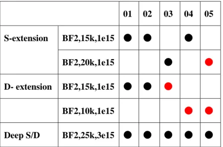
The major split conditions explored in this work are listed in Table 2.1. Different implantation conditions are employed to form the source/drain(S/D)-extension regions. Other implant conditions, including well implantation, channel stop implantation, threshold voltage adjustment implantations, and anti-punch through implantations are shown in Table 2.2.
2-2 Double Patterning
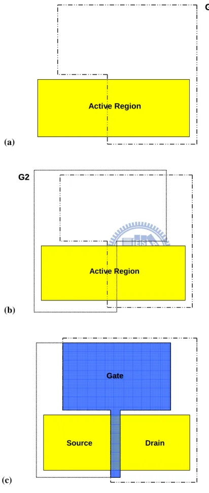
The design of the double patterning masks is shown in Fig. 2.2. The G1 mask covers mainly the right side of the active region capped with the poly-Si serving as the gate material, while the G2 mask covers mainly the left side of the active region. The overlapped region of the two masks defines the gate electrode, and the gate length could be smaller than the limitation of the I-line stepper, i.e., below 0.3 mμ .
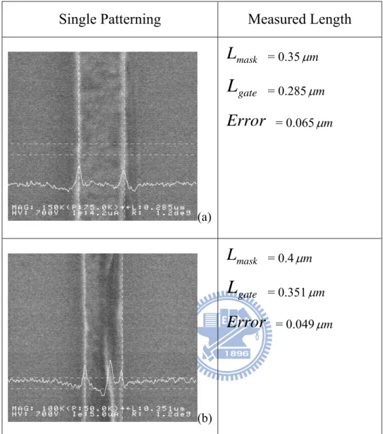
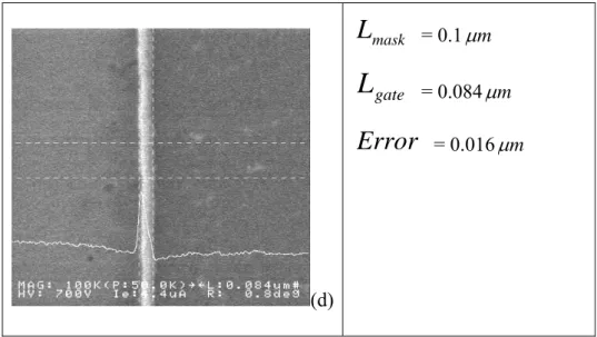
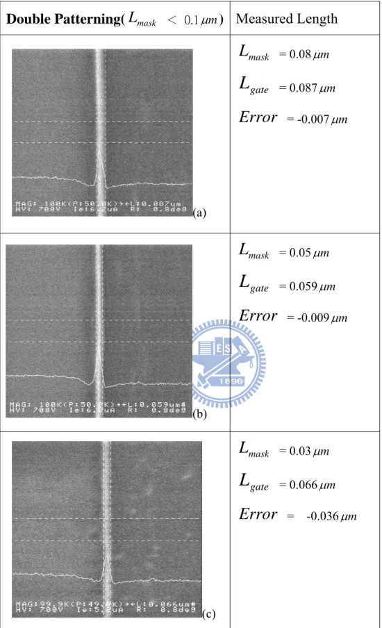
Figure 2.3 shows the after etching inspection (AEI) images with in-line scanning electron microscope (SEM). Here, Lmask is the designed length on the poly-Si etch
mask, andLgate is the practical physical length through lithography and etching
processes. Figures 2.3 (a) and (b) are samples formed with conventional single patterning. From the results, it is observed that the error of gate lenth is more than 10 %. From the results shown in Fig. 2.4, it is confirmed that the double patterning can define the gate length below 0.3 mμ . However, in the figures we can also see that the
gate
L is typically shorter than theLmask.In this study for device characterization, we
used in-line SEM to determine the exact channel length. From the asymmetry in the signals of the secondary electron-emission presenting at the two sides of the poly-Si
gate shown in the figures, the height at the opposite side of the gate seems different. This might be due to the difference in etching rate of the two individual etching steps. In contrast, the image with the single patterning does not exhibit this feature, as shown in Fig. 2.3(a).
Since Lgate is dependent on the lithography and etching biases, Lgatecan be
either longer or shorter thanLmask. There are also process tolerances associated with gate
L . For the same Lmask design, Lgatemay vary from die to die and wafer to wafer.
Though Lgate can be measured with SEM, there is also an uncertainty in the precise
definition of Lgate when the poly-Si etch profile is not vertical. In Fig. 2.3, 2.4, 2.5,
and 2.6 are the measured length of conventional single patterning of different range of gate length are shown, the differences between Lmask and Lgate is defined by the
following equation:
gate
mask
L
L
Error
=
−
(2-1).As shown in Figs. 2.3(a) and (b), the error of single-patterning is around 0.05 mμ . Nevertheless, as shown in Fig. 2.4, the error of double-patterning is below 0.05 mμ , and can be controlled under 0.02 mμ for designed
L
mask dimension in the range from 0.1 mμ to 0.3μm. The results shown in Fig. 2.5 also indicate that the error ofdouble-patterning is small for
L
mask>0.3 mμ . Figure 2.6 shows the images of AEI patterns taken with in-line SEM for double-patterning structures withL
mask < 100 nm, and the error can be controlled below 0.02 mμ . The above results confirm that double-patterning technique can indeed serve the purpose for producing patterned gate with length below 0.1 mμ , much smaller than the limit of resolution restricted bythe exposure machine.
Based on the double-patterning technique, effects of asymmetric S/D-extension could be studied by varying the implantation energy (Table 2.1) in the device fabrication. Four types of devices with various S/D-extension shown in Fig. 2.7 were fabricated and studied in this thesis.
2-3 Electrical Measurement Setup and Basic Electrical Parameters
Current-Voltage (I-V) and capacitance-Voltage (C-V) characteristics were evaluated by using an HP 4156A precision semiconductor parameter analyzer and an HP 4284 LCR meter, respectively. The equivalent oxide thickness (EOT) of the gate dielectrics was obtained from high frequency (100 kHz) C-V curves. The capacitance in strong accumulation becomes independent of the fundamental device parameters; such as bulk dopingNsub, poly-Si gate dopingN , oxide charges p Q , and fast ox
interface statesD . Therefore,it EOTcan be extracted with high confidence from one measured point from the strong accumulation region. [11].
From the Id-Vg curve measured at a drain voltage of -0.05 volt, the characteristics of PMOSFET including threshold voltage (V ), subthreshold swing th
(SS), and transconductance (g ) are extracted according to their definitions as m
follows [1]:
The threshold voltage is defined by using the constant current method, i.e., the gate voltage (V ) needed to achieve a drain current (G ID) of (
( )
nAL
L
W
nA
I
V
V
th=
g d=
1
×
(2-2).Subthreshold swing (SS) can be calculated from the subthreshold current in the weak inversion region by
⎟⎟
⎠
⎞
⎜⎜
⎝
⎛
∂
∂
=
)
log(Id
Vg
SS
(2-3).The transconductance (g ) is extracted by the differentiation of m I to d V , i.e., g
Vg
Id
g
m∂
∂
=
(2-4).The parameters shown above are the basic electrical parameters, more information of devices characteristics is extracted in the final part of Chapter 3.
Chapter 3 Results and Discussion
3-1 Issues on Double Patterning
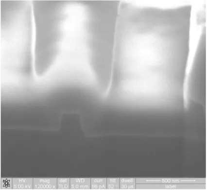
The etched profile of the double-patterning poly-Si gates is examined by the Focus Ion Beam (FIB). Figure 3.1 shows the cross-sectional view of a gate with Lmask
of 0.3 mμ . The practical gate length from the image is around 0.2 mμ to 0.25 mμ . It is observed that the two sides of the poly-Si gate show different slopes and profile.
Besides, the bottom of the right side is lower than that of the left, indicating the (second time) etching of poly-Si is not well controlled and results in undesired recess into the underlying gate oxide and substrate in the region adjacent to the right side of the poly-Si gate. The difference between two levels is around 50nm. For some unknown reason, the etch selectivity between the poly-Si and oxide seems to be lost, rendering such outcome.
Figure 3.2 shows the cross-sectional view of a gate with nominal gate length of 0.2 mμ . The physical length of the poly-Si gate is about 0.1 mμ . The mismatch of the etched profile between two sides of poly-Si gate is more obvious than the result shown in Fig. 3.1. The shape of the poly-Si gate looks more like trapezoidal rather than rectangular as that shown in Fig. 3.1 and Fig. 3.2 in which the nominal gate length is 0.5 μm. The inaccuracy due to the mismatch of the etched profile becomes more profound as the gate length decreases, especially for length below 0.3μm. In contrast, the conventional single-patterning poly-Si gate shown in Fig. 3.4 is far more symmetric and the inaccuracy of the gate length is reduced.
Figure 3.5 is the schematic diagram of the ideal etched profile of poly-Si gate. However, in this work, the double patterning causes the asymmetric etched profile as shown in Fig. 3.6. Obviously the second etching step needs to be improved. The recessed Si substrate in active region destructs the planar structure of MOSFET and may cause dramatic degradation on the device. Certainly an increase in gate oxide can help address the issue, but this violates the scaling trend and is not appropriate for practical applications.
The above phenomenon is postulated to be related to the plasma properties of the transformer coupled plasma (TCP) poly-Si etcher. Owing to the mask design, the percentage of wafer area exposed to the plasma is high and allows us to end the first etching step with end point detection (EPD) mode. Therefore the etching procedure would finish promptly as the underlying thermal oxide layer is exposed. However, in the second etching step the etched (poly-Si) area is much reduced so the optical signal related to etching product becomes too weak to be detected signal and thus only time mode is available for controlling the etching procedure. This is believed to be the main reason for the occurrence of the above phenomenon. Understanding this issue, modified mask design to enhance the optical signal by increasing the etch area in the 2nd etching step will be adopted to address the problem.
3-2 Basic Electrical Characteristics
Two modes of biasing the asymmetrical PMOSFET structure are shown in Fig. 3.7. According to the standard test configuration for PMOSFET, the source is
grounded while the drain is biased with a negative voltage. [1] So, in the forward mode shown in the Fig. 3.7 the side with a shallower extension serves as the drain, and in the reverse mode the drain is switched to the side with deeper extension.
Figure 3.8 (a) shows the transfer characteristics of an asymmetric PMOSFET of Type C. The channel length is 0.3 μm. In the figure the solid lines represents the
forward mode while the dashed lines represents the reverse mode. We can observe that the forward mode has slightly better characteristics in terms of higher drive current and transconductance. The sub-threshold swing (SS) is about 86 mV/decade. The drain induced barrier lowering (DIBL) of forward mode is about 58 mV/V while the reverse mode is 65 mV/V. DIBL is also better with the forward mode. However, the differences mentioned above are not significant as expected. Dependences of DIBL and transconductance versus channel lengths are discussed later in Sec. 3-3. Fig. 3.8 (b) shows the transfer characteristics of a Type-D device with channel length the same as the device characterized in Fig. 3-8(a). In the figure we can see that the forward mode and reverse mode have more appreciable difference in DIBL. As described in last chapter, Type-D device has deeper source extension than Type-C under forward mode of operation. This explains the more profound DIBL difference between the two modes in Fig. 3-8(b).
As can be seen in Fig. 3.8 (c), the transfer characteristics of channel length below 0.3 μm show significantly punch-through behavior. The gate loses effective control of
the channel, especially as a high drain bias is applied. The etch-induced recession mentioned above is certainly one of the factors responsible for the damage.
Additional techniques for suppressing the short-channel effects should be introduced to reach the short channel below 0.1 μm.
Figure 3.9(a) shows the output characteristics of a nominal symmetrical PMOSFET, which uses double-patterning technique to define the gate length and the extensions at two sides are designed with the same depth. However, difference in drive current between the two modes is observed and the reverse mode shows degraded drive current as much as 9%. Figure 3.9 (b) shows the output characteristics of an asymmetric Type-C PMOSFET with identical channel length. As mentioned in Chapter 2, the drain extension of this device was formed with a relatively low implantation energy of 10 keV. In this case the reverse mode further degrades the drive current by the maximum value of 24 %.
The degradation of the drive current is resulted from the increase in the source-drain series resistance. In the discussion of long channel MOSFET current, usually the effect of S/D resistance can be ignored. However, in a short-channel device, the source-drain resistance can be an appreciable fraction of the total series resistance. Theoretically the nominal symmetrical device characterized in Fig. 3.9(a) should not exhibit asymmetrical I-V characteristics shown in the figure. From the SEM analysis given in last section, obviously the degradation in reverse mode is caused by the asymmetrical etched profiles of the double patterning technique. The asymmetrical extension profile would further worsen the situation, as evidenced in Fig. 3.9(b).
circuit shown in Fig. 3.10. A source resistanceR and a drain resistances R are assumed d
to connect an intrinsic MOSFET to the external terminals where V andds Vg are
applied. The internal voltage areVds'andVgs'for the intrinsic MOSFET. One can write the following relations:
ds d s ds ds
V
R
R
I
V
'
=
−
(
+
)
(3.1), s ds g gsV
I
R
V
'
=
−
(3.2).According to the above equations, when a MOSFET is operated, the decrease in the overdrive voltage Vgs' is mainly affected by the source resistance. While
operating in saturation region, the drive current is correlated with overdrive voltage (Vgs’-Vth) rather than the drain voltage. In other words, the drive current is affected
more seriously by the source resistance. In Fig. 3.9(a), the degradation under reverse mode indicates the recessed side contributes more resistance than the other side. This is reasonable, since the recessed junction has a longer distance (along the sidewall of the recess region) to reach the channel edge, as shown in Fig. 3.6. Additional degradation is observed in Fig. 3.9(b) for the asymmetrical device due to the shallower extension depth in the recessed side.
Figure 3.11 (a) and (b) is the output characteristics of the devices with nominal symmetrical S/D and Type-C devices, respectively, measured with a relatively wide drain bias range to illustrate the breakdown behavior. The channel length is 0.3 mμ . As can be seen from the figures, breakdown occurs in the short-channel MOSFET when the drain voltage exceeds a certain value. For the nominal symmetric PMOSFET, difference between the breakdown voltage of forward mode and reverse
modes is small. For the asymmetric MOSFET, though the difference of breakdown voltage between the two modes is also small, the breakdown current of reverse mode is appreciably higher than that of the forward mode. This implies that forward mode has better hot carrier reliability than the reverse mode. Although in this work the unexpected etch-induced recessed phenomenon occurred, it is still confirmed that a reduction in the depth of drain extension junction region during operation can improve the hot carrier reliability. Substrate current can be another indicator for the hot carrier effect. From Fig. 3.12, substrate current of reverse mode is higher than that of forward mode for the asymmetrical device characterized in Fig. 3.11(b). The breakdown process in a PMOSFET is shown in Fig. 3.13. In the process the holes gain energy from the field as they move forward along the channel. Before losing energy through collisions, a number of the holes posses high kinetic energy and are capable of generating secondary electrons and holes by impact ionization. The generated holes are attracted to the drain, adding to the drain current, while the electrons are collected by the substrate contact, resulting in a substrate current. The substrate current in turn can produce a voltage drop from the spreading resistance in the bulk, which tends to forward-bias the source junction. This lowers the threshold voltage of the MOSFET and triggers a positive feedback effect, which further enhances the channel current. The results shown in Fig. 3.11(b) and 3.12 confirm that a shallower drain extension can indeed reduce the field strength in the channel and suppress the associated hot-carrier effects.
Serious poly-Si gate depletion effect is observed. The capacitance in the inversion region does not return to the maximum oxide capacitance recorded in the accumulation region. Instead, the inversion capacitance exhibits a local maximum value, Cmax, at Vg of around -1.5V. This is a feature of poly depletion effect [1], and
the local maximum capacitance is dependent on the effective doping concentration of the poly-Si gate. The higher the doping concentration, the less profound the gate depletion effect is and the local maximum capacitance becomes closer to the oxide capacitance. Based on the analysis of poly-Si depletion effect [1], the relationship between Cmax and the doping concentration of the poly-Si gate, Np, can be extracted
from the following equation:
p i ox
q
N
kT
C
C
max S 28
1
1
ε
+
=
, (3.3).From the equation, the active doping concentration is about 2×10¹⁸ −3
cm ,
which is far less than the typical value (~1020cm-3) in the poly-Si gate. This might be related to the activation step which was carried out with spike-RTA anneal with maximum temperature of 1000 ℃. Further optimization in the activation step is
needed to suppress such effect.
3-3 Short Channel Effects
Figure 3.15 shows the threshold voltage (V ) roll-off of the three types of th
asymmetric PMOSFETs. V is extracted at a drain voltage of -0.05 V. From the th
appreciable difference in threshold voltage between the forward mode and reverse mode. This implies that changing the depth of S/D extension junctions causes no effects on the Vth roll-off control. This is probably due to the fact that the minimum channel length (0.3 μm) is not short enough to distinguish the effect of junction depth.
Moreover, the recess phenomenon occurs in the second etching step may also affect. However, the DIBL effect characterized at a high drain bias could resolve the effect of junction depth, which is shown later.
Figure 3.16 shows the V roll-off of Type-A devices fabricated with either th
single patterning or double patterning. As can be seen in the figure, the single patterning split shows reverse short-channel effect which is not observed in the double patterning devices. Note that the double patterning split is nominal symmetrical, although in fact they are asymmetrical due to the occurrence of etch-induced recess phenomenon induced at the drain side. This could be the reason why the reverse short-channel effect is not observed in the split, since the practical drain junction depth is deepened with the recess.
Figure 3.17 compares the delta V roll-off of Types A~D fabricated with th
double patterning, together with the single-patterned symmetric MOSFET. Obviously the Vth roll-off trends for all the asymmetrical devices fabricated by
double-patterning process are similar and worse than the Type-A splits, it is convinced that the recess of right side edge in the vicinity of poly-Si gate draws impact on the short-channel effect control. Figure 3.6 is the schematic diagram of double-patterning poly-Si gate. The over-etched active region circled by red dashed line may expose the
Si sidewall near the poly-Si edge. The un-gated region may degrade the effective control region from the point of views of charge-sharing model.
Transconductance is also extracted from the transfer Id −Vg curve measured in
the linear region, and the results are shown as a function of channel length in Fig. 3.19. In the figure, the transconductance of Type C is slightly lower than the other types, owing to their most shallow source and drain extension depth among all splits (see Fig.2.4). DIBL versus channel lengths for the Type C devices is also characterized and shown in Fig. 3.20. It is seen that the forward mode shows better DIBL than reverse mode as channel length is below 0.5 mμ , an indication demonstrating the effect of the asymmetrical S/D structure.
Chapter 4 Conclusion and Future
Works
4-1 Conclusion
In this study, the double-patterning technique has been proved to be a feasible method for generation of gate patterns with length below 0.1 mμ using a conventional I-line stepper. In comparison with the conventional single patterning, double-patterning technique needs one more mask to pattern the gate length, but the inherent asymmetrical S/D formation process makes the fabrication more flexible and more freedoms for device optimization. However, the etch-induced recess at one side of the gate during the second gate-etch step remains to be addressed. This phenomenon results in additional resistance in the drain side leading to asymmetric output characteristics. Besides, the recess etched substrate degrades the short-channel control.
Note the endpoint signal of TCP in the second gate-etch step is not detectable and thus the etching step can not be promptly stopped. Such issue can be overcome by modifying the mask design to increase the etched area and therefore the end pint signal during etching. Otherwise, the control of the gate length and etched profile could be the main issue for the double patterning technique.
In case the above issue is solved, with the double patterning technique, the MOSFET with optimized asymmetrical S/D design could be feasible. Different requirements for source and drain junctions could be realized by the added mask.
Improved device performance in terms of higher immunity to short-channel effects and better current drive is expected.
4-2 Future works
In this work, the PMOSFETs with asymmetric S/D extensions and channel length of 0.3 mμ .have been fabricated and characterized. Nevertheless, to fabricate the short channel devices with gate length below 0.1 mμ , some practical suggestions are listed as follows:
(1) Add halo implantation to suppress the punch-through effect. From this work, devices with channel length below 0.3 mμ suffer from punch-through effect, a tilt angle implantation could be introduced to prevent it. And single side halo implantation could also be introduced. Theoretically, only drain side needs halo implantation.
(2) Mask modification. Since with the present design the second etching cannot detect the end point signal, the control of poly-Si gate etch process is not satisfactory. With mask modification, the area of poly-Si to be etched in the second gate-etch step would be significantly increased and thus the EPD mode could be executed to improve the process control.
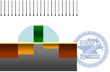
Fig. 2.1 (a) Deposition of 200 nm un-doped poly-Si layer after forming the 3 nm gate oxide with thermal oxidation.
Fig. 2.1 (b) The G1 lithographic step to generate the PR patterns and the subsequent etching step to transfer the patterns into the polysilicon.
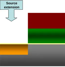
Source extension
Source extension
Fig. 2.1 (c) Source-side extension implant. The PR is removed after source-extension implantation.
Fig. 2.1(d) The G2 lithographic step to generate the PR patterns.
Drain extension
Drain extension
Fig. 2.1 (e) The etching step to define the polysilicon gate. Drain-side extension implant is subsequently performed.
Fig. 2.1 (g) Deposition of a 80 nm TEOS layer.
(a) Active Region G1 Active Region G1 (b) Active Region G2 Active Region G2 (c) Source Drain Gate Source Drain Gate Gate
Single Patterning
Measured Length
(a) maskL
= 0.35 mμ gateL
= 0.285 mμError
= 0.065 mμ (b) maskL
= 0.4 mμ gateL
= 0.351 mμError
= 0.049 mμFig. 2.3 In-line SEM images and measured length for patterns formed with single patterning proces
Double Patterning
(
0.1 mμ ≦L
mask < 0.3 mμ)
Measured Length
(a) maskL
= 0.2 mμ gateL
= 0.182 mμError
= 0.018 mμ (b) maskL
= 0.2 mμ gateL
= 0.19 mμError
= 0.01 mμ (c) maskL
= 0.1 mμ gateL
= 0.087 mμError
= 0.02 mμ(d) mask
L
= 0.1 mμ gateL
= 0.084 mμError
= 0.016 mμFig. 2.4 In-line SEM images and measured length for patterns formed with double patterning process (0.1 μm ≦ Lmask < 0.3 μm).
Double Patterning(
L
mask > 0.3 mμ)
Measured Length
(a) maskL
= 0.5 mμ gateL
= 0.498 mμError
= 0.002 mμ (b) maskL
= 0.4 mμ gateL
= 0.389 mμError
= 0.011 mμ (c) maskL
= 0.3 mμ gateL
= 0.309 mμError
= -0.009 mμFig. 2.5 In-line SEM images and measured length for patterns formed with double patterning process (Lmask≧ 0.3 μm).
Double Patterning(
L
mask < 0.1 mμ) Measured Length
(a) maskL
= 0.08 mμ gateL
= 0.087 mμError
= -0.007 mμ (b) maskL
= 0.05 mμ gateL
= 0.059 mμError
= -0.009 mμ (c) maskL
= 0.03 mμ gateL
= 0.066 mμError
= -0.036 mμFig. 2.6 In-line SEM images and measured length o for patterns formed with double patterning process (Lmask < 0.1 μm).
Fig. 2.7 (a) Device Type A as the control samples with symmetric S/D.
Fig. 2.7 (b) Device Type B with deep source- extension.
Fig. 2.7 (c) Device Type C with shallow drain-extension.
Table 2.1 Split conditions of the PMOSFETs fabricated with double-patterning process. Wafer No. 01 and 02 are Type A (or control samples), 03 is Type B, 04 is Type C, and 05 is Type D shown in Fig. 2.8.
Ion Energy (eV) Dose (cm-2)
N-Well P+ 120K 7.5e12
Channel Stop As+ 120K 3e12
Vth As+ 80K 1e13
APT P+ 120K 4e12
Table 2.2 Other major implantation conditions used in the PMOSFET fabrication.
01 02 03 04 05 BF2,15k,1e15 ● ● ● S-extension BF2,20k,1e15 ● ● D- extension BF2,15k,1e15 ● ● ● BF2,10k,1e15 ● ● Deep S/D BF2,25k,3e15 ● ● ● ● ●
Fig. 3.1 FIB image of a double patterning gate with nominal length Lmask= 0.3μ . m
Fig. 3.3 FIB image of a double patterning gate with nominal length Lmask= 0.5μ m
Fig. 3.5 The schematic diagram of a conventional MOSFET adopting single -patterning.
Fig. 3.6 The schematic diagram of the double-patterning MOSFET.
N-Sub. Gate P+ P P+ - P -Vd GND Vg GND (a) Forward mode
Vgs(V) -2.0 -1.5 -1.0 -0.5 0.0 0.5 Ids (A) 1e-15 1e-14 1e-13 1e-12 1e-11 1e-10 1e-9 1e-8 1e-7 1e-6 1e-5 1e-4 1e-3 gm (μ S) 0 2e+1 4e+1 6e+1 8e+1 (a) Vgs (V) -2.0 -1.5 -1.0 -0.5 0.0 0.5 Ids (A) 1e-15 1e-14 1e-13 1e-12 1e-11 1e-10 1e-9 1e-8 1e-7 1e-6 1e-5 1e-4 1e-3 Forward Reverse (b)
W=10
μm L=0.2 μm
Vgs(V) -2.0 -1.5 -1.0 -0.5 0.0 0.5 I ds (Α ) 1e-7 1e-6 1e-5 1e-4 1e-3 1e-2 1e-7 1e-6 1e-5 1e-4 1e-3 1e-2 Vd= -0.05V Vd= -1.5V (c)Fig. 3.8 (a) Sub-threshold characteristics and transconductance of type C and (b) type D PMOSFET under forward and reverse modes of operation. L = 0.3μm, W= 10μm. (c) Sub-threshold characteristics of a short-channel PMOSFET. L= 0.2μm, W=10μ
Vds (V) -2.0 -1.5 -1.0 -0.5 0.0 Ids (A) -0.0030 -0.0025 -0.0020 -0.0015 -0.0010 -0.0005 0.0000 0.0005 Forward Reverse Vgs-Vth= 0~ -2V, step= -0.5V 9% (a) Vgs-Vth=0 ~ -2V, step= -0.5V Vds (V) -2.0 -1.5 -1.0 -0.5 0.0 Ids (A) -0.0018 -0.0016 -0.0014 -0.0012 -0.0010 -0.0008 -0.0006 -0.0004 -0.0002 0.0000 0.0002 Forward Reverse 24% (b)
Fig. 3.9 Id − characteristics of (a) a nominal symmetric and (b) an asymmetrical Vd
PMOSFET fabricated with double patterning technique under forward and reverse modes of operation. L= 0.3 μm, W = 10 μm.
Sym. PMOSFET,Vgs-Vth=0 ~ -2V, step= -0.5V V ds (V) -6 -5 -4 -3 -2 -1 0 I ds (A) -0.0030 -0.0025 -0.0020 -0.0015 -0.0010 -0.0005 0.0000 Forward Reverse (a)
Asym. PMOSFET, Vgs-Vth = 0 ~ -2V, step=-0.5V
Vds (V) -6 -4 -2 0 I ds (A) -0.012 -0.010 -0.008 -0.006 -0.004 -0.002 0.000 Forward Reverse (b) Fig. 3.11 Id − characteristics of (a) a nominal symmetric and (b) an asymmetrical Vd
Asymmetric PMOSFET, Vgs-Vth= 0 ~ -2V, step=-0.5V Vds (V) -6 -4 -2 0 Isu b (A) 5.0e-4 1.0e-3 1.5e-3 2.0e-3 2.5e-3 3.0e-3 3.5e-3 Forward Reverse
Fig. 3.12 Isub−Vdcharacteristics of the asymmetric PMOSFET characterized in Fig.
3.11(b) under forward and reverse modes of operation.
sat ds
ds
V
V
>>
_L=50um, W=50um Vg(V) -2 -1 0 1 2 3 C(F) 1.0e-11 1.2e-11 1.4e-11 1.6e-11 1.8e-11 2.0e-11 2.2e-11 2.4e-11 2.6e-11 2.8e-11 3.0e-11 3.2e-11
Fig. 3.14 Measured capacitance-voltage (C-V) characteristics of an asymmetric PMOSFET. The measurement frequency is 100 kHz
Type B Lmask(μm) 0.1 1 10 Vth (V) -1.2 -1.0 -0.8 -0.6 -0.4 -0.2 0.0 -1.2 -1.0 -0.8 -0.6 -0.4 -0.2 0.0 Forward Mode Reverse Mode (a) Type C Lmask(μm) 0.1 1 V th (V) -1.2 -1.0 -0.8 -0.6 -0.4 -0.2 0.0 -1.2 -1.0 -0.8 -0.6 -0.4 -0.2 0.0 Forward Mode Reverse Mode (b)
Type D Lmask(μm) 0.1 1 10 Vth (V) -1.2 -1.0 -0.8 -0.6 -0.4 -0.2 0.0 -1.2 -1.0 -0.8 -0.6 -0.4 -0.2 0.0 Forward mode Reverse mode (c)
Fig. 3.15 Threshold-voltage (Vth) roll-off of(a) Type B, (b) Type C, and (c) Type D
devices. Vth is extracted at Vd of -0.05 V under forward mode and reverse mode,
respectively. ΔVth Roll-Off Lmask(μm) 0.1 1 10 Δ V th (mV) -200 -100 0 100 200 300 -200 -100 0 100 200 300 Type A (Single-patterning) Type A (Double-pattering)
Fig. 3.16 Short-channel effects of Type-A devices fabricated with single-patterning and double patterning.
Linear threshold Lmask(μm) 0.1 1 10 Δ Vth (m V ) -200 -100 0 100 200 300 400 Type A(Double-patterning) Type B Type C Type D
Type A(Single patterning)
Fig. 3.17 Short-channel threshold voltage roll-off effects for all types of structures. Threshold voltages are measured at low drain voltage. Type A with double-patterning (open circle symbols), Type B with double-patterning (triangle symbols), Type C with double-patterning (rectangular symbols), Type D with double-patterning (diamond symbols), Type A with single-patterning (star symbols) are also shown.
gm_Max Lmask(μm) 0.1 1 10 T ransconductance(ms) 0 2e-2 4e-2 6e-2
8e-2 Type A(Double-patterning)
Type B Type C Type D
Type A(Single-patterning)
Fig. 3.18 Measured transconductance versus channel length for all splits of devices.
Fig. 3.19 Measured DIBL versus channel length under forward mode (circle symbols) and reverse mode (triangle symbols) for Type C devices.
Type C L mask (μm) 0.1 1 10 DIBL (mV /V) 0 20 40 60 80 100 120 Forward Mode Reverse Mode
References
[1] Y. Taur, and T. H. Ning, “Fundamentals of Modern VLSI Devices,” Cambridge University Press, 1998.
[2] S. Ogura, P. J. Tsang, W. W. Walker, D. L. Critchlow, and J. F. Sherpard, “Design and characteristics of the lightly doped drain source (LDD) insulated
gate field effect transistor,” IEEE Trans. Electron Devices, vol. ED-27, p. 1359,
1980.
[3] S. Ogura, C.F. Codella, N. Rovedo, and J. F. Shepard, “A half micron MOSFET
using double implanted LDD,” Symp. on VLSI Tech. Dig., p. 42, 1982.
[4] R. Izawa, T. Kure, S. Iijima, and E. Takeda, “The impact of gate-overlapped
LDD (GOLD) for deep submicron VLSI’s,” IEDM Tech. Dig., vol.33, pp. 38-41,
1987.
[5] T. Horiuchi, T. Homma, Y. Murao, K. Okumura, “An asymmetric sidewall
process for high performance LDD MOSFET’s,” IEEE Trans. Electron Devices,
vol. 41, pp. 186-190, 1994.
[6] J.F. Cheng, J. Tao, P. Fang, C. Hu, “Performance and reliability comparison
between asymmetric and symmetric LDD devices and logic gates,” IEEE Journal
of Solid-State Circuits, Vol. 34, pp. 367-371, 1999.
[7] T. Ewert, L. Vestling, and J. Olsson, “Investigation of the electrical behavior of
an asymmetric MOSFET,” Microelectronic Engineering , pp. 428–438, 2003.
[8] T. N. Buti, S. Ogura, N. Rovedo, and K. Tobimatsu, “A new asymmetrical halo
source GOLD drain (HS-GOLD) deep sub-half-micrometer n-MOSFET design for reliability and performance,” IEEE Trans. on Electron Devices, vol. 38, pp.
[9] M. Drapeau, V. Wiaux, E. Hendrickx, and S. Verhaegen,“Double patterning
design split implementation and validation for the 32nm node,” Proc. of SPIE,
Vol. 6521, 652109, 2007.
[10] A. Vanleenhove, and D. V. Steenwinckel, “A litho only approach to double
patterning,”Proc. of SPIE, Vol. 6520, 65202F, 2007.
[11] R. Rios , and N. D. Arora, “Determination of ultra-thin gate oxide thicknesses for
CMOS structures using quantum effects,” IEDM, p.613, 1994.