國 立 交 通 大 學
電子工程學系電子研究所
碩 士 論 文
利用通道背向散射理論及溫度係數模型分析奈米
級金氧半電晶體電子遷移率的劣化之研究
Analysis of Mobility Degradation in Nanoscale
DG nMOSFETs Using Channel Backscattering
Theory and Temperature Coefficient Method
研 究 生:詹益先 Yi-Hsien Chan
指導教授:陳明哲 Prof. Ming-Jer Chen
利用通道背向散射理論及溫度係數模型分析奈米
級金氧半電晶體電子遷移率的劣化之研究
Analysis of Mobility Degradation in Nanoscale
DG nMOSFETs Using Channel Backscattering
Theory and Temperature Coefficient Method
研 究 生: 詹益先
Student: Yi-Hsien Chan
指導教授: 陳明哲
Advisor: Ming-Jer Chen
國 立 交 通 大 學
電子工程學系 電子研究所
碩 士 論 文
A Thesis
Submitted to Department of Electronics Engineering & Institute of Electronics College of Electrical and Computer Engineering
National Chiao Tung University in Partial Fulfillment of the requirements
for the Degree of Master in
Electronic Engineering September 2010
Hsinchu, Taiwan, Republic of China
i 利用通道背向散射理論及溫度係數模型分析奈米級金氧半電晶體電 子遷移率的劣化之研究 研究生: 詹益先 指導教授: 陳明哲博士 國立交通大學 電子工程學系電子研究所 摘要 近年來許多的研究指出,當金氧半場效電晶體的元件尺寸縮減到 數百奈米至數十奈米時,電子遷移率將隨通道長度減少而遞減。研究 指出此電子遷移率的降低是因為載子在元件中有其所對應的飽和速 度,其載子將無法超越此一速度。所以此篇論文主旨在於探討當元件 尺寸縮減時,將面臨平衡態區域範圍的縮減。因此我們利用的模擬軟 體 TCAD 模擬奈米級雙閘極電晶體的特性,其中我們考慮了擴散飄移 模型以及量子效應。在此我們為了獲得其不受飽和速度影響的電子遷 移率,必須要在極小的汲極偏壓下模擬。除此之外利用通道背向散射 理論來解釋其飽和速度的現象,並且利用其隨溫度變化的特性來加以 分析。最後比較模擬的臨界散射長度以及計算值間的差異性,加以修 正而得其合理之結果。
ii
Analysis of Mobility Degradation in Nanoscale DG nMOSFETs Using Channel Backscattering Theory and Temperature Coefficient
Method
Student: Yi-Hsien Chan Advisor: Dr. Ming-Jer Chen
Department of Electronics Engineering Institute of Electronics
National Chiao Tung University
Abstract
In recent years, many investigations point out that mobility would degrade with the channel length scaling down in nanoscale MOSFETs. It is suggested that the reason for the mobility degradation is caused by the corresponding saturation velocity. The carrier velocity cannot excess this limit in nature. Therefore, we focus on the exploration of the mobility decrease in drain current linear region with channel length shrinkage. First, we simulate the DG nMOSFET characteristics by using TCAD simulator. In the simulation, we consider the drift-diffusion model and quantum effect. In order to extract the real mobility at equilibrium condition, we simulate the case at VD=1mV. Furthermore, we use the channel backscattering theory to explain the effect of saturation velocity and use the temperature coefficient method to analyze the variation between the two methods. Finally, we compare the error of the critical scattering length between the simulation result and the calculation result, along with the correction to get a feasible result.
iii
誌 謝
在我就讀碩士班的這兩年來,雖不可稱得上一帆風順,但在陳明 哲老師的指導下,讓我順利低完成碩士學業。在此感謝陳明哲老師孜 孜不倦的指導,並且提供良好的研究環境與資源,讓我收穫頗多。此 外,感謝謝振宇、李建志、許智育以及李韋漢學長們總是親切低在這 兩年來提供各方面的協助與指導,以及湯侑穎學長與我共同奮鬥了一 年。也謝謝蔡濬澤、鄭寬豪與張華罡三位同學與我在老師的帶領下互 相勉勵,學習成長,一起度過了很多在實驗室趕進度挑燈夜戰的時光。 實驗室的學弟妹也在平常提供了不少協助,並帶給實驗室很多活力與 歡樂。特別要感謝光心君學妹與彭霖祥學弟,在研究上對我幫助良多。 最後要感謝我的父母朋友們,作為我的後盾以及支柱,讓我能無後顧 之憂的完成碩士學業。最後謝謝口試委員(林鴻志教授以及張智勝博 士)所給予的寶貴意見,讓我完成一份更好的論文。 2010 年 9 月詹益先
iv
Contents
Abstract (Chinese)………...i Abstract (English)………..ii Acknowledgement……….iii Contents……….iv List of Captions……….vi List of Symbols………ixChapter 1 Introduction
………...………...1Section 1.1 Structure of the Simulated Device………...1
Section 1.2 Models of Simulation………...………...1
Section 1.3 Analysis and Theories……….…………..…...2
Section 1.4 Thesis Organizations.………...……...3
Chapter 2 Channel Backscattering Theory.
...4Section 2.1 Introduction...4
Section 2.2 Channel Backscattering Theory...4
Section 2.3 Mean Free Path and Critical Scattering Length...7
v
Section 2.5 Conclusion…...9
Chapter 3 Analysis of TCAD simulation result
…………...10Section 3.1 Introduction…...………...10
Section 3.2 Extraction of Five Temperature Coefficients …………...10
Section 3.2.1 Schrödinger–Poisson–Drift–Diffusion (SPDD) model…..10
Section 3.2.2 Channel Status at Equilibrium………....12
Section 3.2.3 Mobility Extraction at Equilibrium………....13
Section 3.2.4 Critical Scattering Length LkT Extraction in Saturation Region (VG=0.8V and VD=1V) ……….…….………....15
Section 3.2.5 Injection velocity vinj Extraction in Saturation Region (VG=0.8V and VD=1V) ………...……….………....16
Section 3.2.6 Inversion Carrier Density Ninv Extraction in Above Threshold Region (VG=0.8 and VD=1mV/ 1V).………...17
Section 3.2.7 Temperature Coefficient of Drain Current in Saturation Region (VG =0.8V and VD=1V) ………...18
Section 3.2.8 Verification of Temperature Coefficient Method…………18
Section 3.3 Extraction of Ballistic Ratio (BR) ………..………..………19
Chapter 4 Conclusion……….
…………...21vi
List of Captions
Fig. 1-1 Schematic illustration of DG MOSFET………..24 Fig. 1-2 Schematic illustration of channel backscattering theory in terms of the conduction band profile. F+: the incident flux from the source is located at the peak of the source-channel barrier. Fb-: the incident flux from the drain. T: the transmission coefficient for the flux cross the barrier for both directions………...………25 Fig. 3-1 The conduction energy band diagram along Y-sirection. T=300K, VD=0V, VG=-0.2V/ 0.8V and LG=90nm……....26 Fig. 3-2 The conduction energy band diagram along the channel. T=300K, VD=1V, VG=1V and LG=15/20/45/90nm………27 Fig. 3-3 The lowest subband E11 along the channel. T=250/ 300/ 350K, LG=15/ 90nm and VD=0/ 1mV. The difference between two different VD is caused by the variation of Fermi-level. ………..…28 Fig. 3-4 Schematic diagram of sheet carriers…………...…………..29 Fig. 3-5 The inversion carrier density, Ninv along the channel. T=250/ 300/ 350K, LG=15/ 90nm and VD=0/ 0.001/ 1V. DIBL gives arise in the carrier density increasing at LG=15nm……...30 Fig. 3-6-1 The inversion carrier density Ninv for VG=-0.2~1V at
LG=15/ 90nm, T=300K and VD=0V of TCAD and Schred..31 Fig. 3-6-2 The inversion carrier density Ninv for VG=-0.5~1V at LG=90nm, T=300K and VD=0V/ 50mV……….…..31
vii
Fig. 3-9-1 Electron Quasi-Fermi Level alone the channel for LG=15/ 20/ 45/ 90nm, VD=1mV and VG=0.8V at Y=0………..32 Fig. 3-8-1 Total resistance for LG=15/ 20/ 45/ 90nm at VD=1mV/25mV and VG=0.8V………..………..…33 Fig. 3-8-2 Source/ Drain resistance for LG=15/ 20/ 45/ 90nm at VD=1mV/ 25mV and VG=0.8V………33 Fig. 3-8-3 C h a nn e l r es is t anc e f o r LG= 1 5 / 20 / 45 / 90 n m a t VD=1mV/25mV and VG=0.8V……….34 Fig. 3-9-1 T h e a p p a r e n t m o b i l i t y f o r LG= 1 5 / 2 0 / 4 5 / 9 0 n m , T=250/300/350K and VD=1mV…………..…………...35 Fig. 3-9-2 T h e a p p a r e n t m o b i l i t y f o r LG= 1 5 / 2 0 / 4 5 / 9 0 n m , T=250/300/350K and VD=25mV…..…………..……...35 Fig. 3-9-3 T h e a p p a r e n t m o b i l i t y f o r LG= 1 5 / 2 0 / 4 5 / 9 0 n m , T=250/300/350K and VD=1/ 25mV……….36 Fig. 3-9-4 The apparent mobility extracted from DD model and calculated from CT model. ………..36 Table 1 Caughey-Thomas formula parameters……….37 Fig. 3-10-1 Profile of the lowest subband energy E11 at VG=0.8V and
VD=1V………38
Fig. 3-10-2 kT-layer extension as a function of the temperature at VG=0.8V and VD=1V……….…..38 Fig. 3-11-1 Injection velocity against the inversion carrier density for three temperatures....……….……….…..39 Fig. 3-11-2 Injection velocity as a function of the temperature at VG=0.8V and VD=1V……….…….…..39
viii
Fig. 3-12-1 Inversion carrier density vs. VG. At X=0 and T=250K…....40 Fig. 3-12-2 Inversion carrier density vs. VG. At X=0 and T=250K...40 Fig. 3-12-3 Inversion carrier density vs. VG. At X=0 and VD=1V……..41 Fig. 3-12-4 Beta for LG=15/ 20/ 45/ 90nm, T=250/ 300/ 350K, VG=0.8 and VD=1V………....41 Fig. 3-13-1 Drain current vs. gate voltage………..42 Fig. 3-13-2 Vt h-LG. Vt h was extracted by using the maximum transconductance method..……….………..42 Fig. 3-13-3 Alpha α against the channel length….…………...………..43 Fig. 3-14 Ratio= α……….44 Fig. 3-15-1 BR for LG=15/ 20/ 45/ 90nm, T=250/ 300/ 350K, VG=0.8 and VD=1V. BR increases with channel length scaling down….45 Fig. 3-15-2 BR for LG=15/ 20/ 45/ 90nm, T=250/ 300/ 350K, VG=0.8 and VD=1V. BR increases with channel length scaling down….45 Fig. 3-15-3 BR (CT model) calculation. Set A [3]:
……….…………46 Fig. 3-16-1 The calculated LkTcal versus temperature for different LG,
along with the extracted LkT……….47 Fig. 3-16-2 The comparison of BR versus channel length for different temperature. BRTC is also shown in the comparison of calculated LkT………...…………....………....47
ix
List of Symbols
Symbol Meaning
LkT critical scattering length xvs virtual source position
F+ injection flux from source to channel Fb
-injection flux from drain to source T+ transmission coefficient for F+ flux T- transmission coefficient for Fb
flux Qinv inversion charge density
Ninv inversion carrier density
vT equilibrium unidirectional thermal velocity vinj injection velocity
RS series resistance at source RD series resistance at drain λ mean free path
0 mobility at equilibrium rc scattering coefficient BR ballistic ratio
nvi degeneracy factor of ith valley mdi density of states effective mass of i
th
valley Ef quasi-Fermi level
Φn electron quasi-Fermi potential function Φp hole quasi-Fermi potential function
temperature coefficient of LkT temperature coefficient of 0 temperature coefficient of vinj
temperature coefficient of drain current
1
Chapter 1
Introduction
Section 1.1 Structure of the Simulated Device
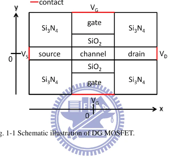
In this simulation, we explore the 2-D double gate n-channel MOSFETs, which were simulated by using the TCAD (Sentaurus) simulator. The simulated devices have four channel length sizes from 90nm to 15nm, drain and source lengths are fixed at 20nm, oxide thickness is 6nm, body thickness is 6nm, poly gate doping concentration is 1020 cm-3 and body doping concentration is 3x1016 cm-3. The simulation bias conditions are: VG=0.8V; VD=0.001V, 0.025V and 1V; and the operating temperature = 250K, 300K and 350K. Fig. 1-1 shows the structure of the simulated device. Metal contacts were set on the left end side of source, the right end side of drain, the upper end of gate, and the bottom end of gate. This forced us to consider the series resistances of highly-doped source and drain region. Since the contact is set as the ohmic contact. Therefore, the contact resistance is neglected.
Section 1.2 Models of Simulation
Usually, doing 2-D simulations would only use drift-diffusion model (DD model). DD model is not suited to analyze SOI structure and short channel structure. Therefore, the accurate prediction of the electrical characteristics of state-of-the-art nanoscale semiconductor devices
2
demands for the inclusion of quantum effects: this effect may cause increased equivalent oxide thickness due to strong electron confinement at Si/SiO2 interface. Some groups have proposed some complicated models or simulated the device at atomic level with Monte Carlo technique. Therefore, in order to get more accurate result in this simulation, we not only used the DD transport model but also appended 1-D Schrödinger–Poisson to confine the y-direction in the channel. The model is so called Schrödinger–Poisson–Drift–Diffusion (SPDD) model proposed in [1]. This gives us a relative correct solution of the analysis on channel status, for instance, sub-threshold swing, energy, and carrier density distribution along the channel. Furthermore, there are three mobility models that can be used to solve the DD transport model: (i) doping dependent mobility; (ii) high-field saturation [4]; and (iii) mobility degradation at interfaces (Enhanced Lombardi Model). The three models are combined by following Mathiessen’s rule. The simulation model (ii) would be used to explain the characteristics of mobility degradation with channel length shrinkage in Chapter 3.
Section 1.3 Analysis and Theories
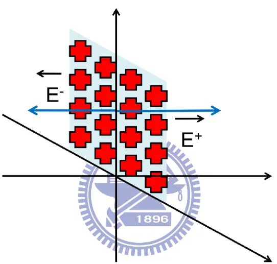
With channel length decreasing to nanoscale, the most important issue we faced is the high field saturation. Fortunately, there is two models proposed to explain the effect: (i) the traditional model called Caughey-Thomas formula [4] suitable to analyze the status along the channel; and (ii) channel backscattering theory proposed by Lundstrom, et al. [2]. By the theory, the barrier position of the lowest sub-band
3
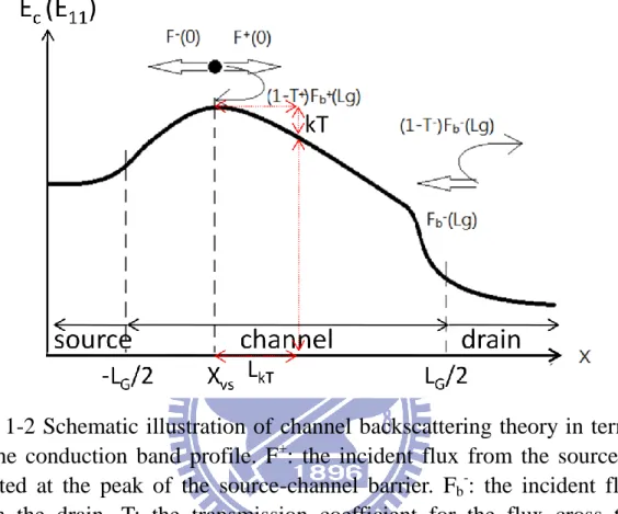
energy called the virtual source point Xvs dominates device characteristic and the critical scattering length. Fig. 1-2 shows a schematic diagram of channel backscattering theory. The status at Xvs can critically determine the device performance. Using the theory, it can help us analyze the effect of mobility degradation and backscattering flux degradation in the scaling direction.
Section 1.4 Thesis Organizations
In this thesis, we explore the phenomenon of mobility degradation and the possibility of applying the channel backscattering theory to the result simulated by traditional transport model with channel scaling down at three different temperatures. The following Chapter 2 will explain the channel backscattering theory and the temperature coefficient method proposed elsewhere [3]. And in Chapter 3, we will show the simulation result and extract the temperature coefficients. Furthermore, we will give the reasons of mobility degradation and compare the errors between the channel backscattering theory and temperature coefficient method. We also will bring up a possible solution to make us the extracted ballistic ratio proper. Finally, we make a conclusion in Chapter 4.
4
Chapter 2
Channel Backscattering Theory
Section 2.1 Introduction
Channel backscattering theory is a simple one-flux scattering theory used in MOSFETs [2], [10], [11], [12]. The theory gives a new expression of current-voltage characteristics used to analyze short-channel devices. The new formula is expressed in terms of scattering parameters rather than a mobility. For long-channel transistors, the results reduce to conventional drift-diffusion (DD) theory. But DD theory also applies to short channel device even as the channel length is shorter than the mean-free-path. In backscattering theory, the transconductance is limited by carrier injection from the source for ultra short channel. Another channel backscattering concept to analyze short channel effect has been proposed by [3] in terms of the Temperature Coefficient Method. In this concept, temperature is used to analyze the variation of channel status for different temperatures. By extracting the mean free path, critical scattering length, the temperature coefficients of mobility, injection velocity and the power law coefficients to define the ballistic ratio.
Section 2.2 Channel Backscattering Theory
With channel scaling down, traditional current model would touch a limit caused by the saturation velocity. The key issue of channel backscattering theory is to maximize the saturation drain current for
5
short-channel devices. Electrons are injected from the source into the channel across a potential barrier varying with the gate voltage and the drain voltage. Traditionally, carriers drift and diffuse across the channel and finally are collected at the drain. Fortunately, TCAD can work well on the 2D simulation. That is we could simply grasp the status on the virtual source point. And drain-induced barrier lowering (DIBL) has been taken into account by using TCAD simulator. In the theory, the virtual source at the barrier height is considered as a carrier reservoir; which injects a flux from the source side across the barrier into the channel. There are not all of the carriers that can transmit across the barrier. A fraction of the flux, rc, goes back to the source. The backscattering region, k-T layer, is the key region which dominates the backscatter flux. As shown in Fig. 1-2, k-T layer is the length from the barrier height to the point with a kT potential drop rather than the barrier point. The length is called critical scattering length, LkT. Physically, the channel length is equal to the critical scattering length at very small drain bias. Therefore, whenever the critical length is larger than the channel length, LkT is assumed to be the same as LG. We can find the corresponding drain current from the backscattering coefficient rc as below. In Fig. 1-2, F
+ is the injection flux from source to channel, and Fb
is the injection flux from drain to source. T+ is the transmission coefficient for F+ flux, and T -is the transm-ission coefficient for Fb
flux. At equilibrium, T -approximates T+=T,
(2-1) (2-2)
6
where is the equilibrium unidirectional thermal velocity (i.e., the average velocity of carrier across the barrier in the positive direction). And position 0 is defined at the Xvs point. From Eq. (2-1) and (2-2), the drain current can be expressed as:
. (2-3)
Under ballistic condition, the negative flux caused by thermal emission from the drain is given by thermionic emission as:
(2-4) (2-5) Substituting Eq. (2-4) and (2-5) into (2-3), we have
. (2-6) And taking the series resistance effect into Eq. (2-6), we can get the drain current at linear and saturation regions:
(2-7)
(2-8)
where is the inversion carrier density per unit area at virtual source, Xvs, point and RS/ RD are the series resistance at the source/ drain. is the thermal velocity for nondegenerate case. For the degenerate case, we use the injection velocity to replace the thermal
7
velocity. The injection velocity can be expressed as
.
Furthermore, rc can be expressed as:
(2-9) is the mean free path and is the mobility extracted at thermal equilibrium. In simulation, DIBL has been included. Therefore, Qinv has DIBL effect in itself.
Section 2.3 Mean Free Path and Critical Scattering Length
The mean free path is a controlling factor to determine the performance of device. It is associated with the mobility and the thermal injection velocity. Besides, the critical scattering length is widely evaluated by each group’s study [5], [6], [14]; that is, how to calculate LkT would really decide the characteristics of device. Therefore, we will slightly correct the critical scattering length by using the direct extraction of LkT from the simulation result.
Section 2.4 Temperature Coefficient Method (TC Model)
In section 2.2, we explained the component of the backscattering coefficient, rc. It can be clearly found that it has some relationship with the temperature. This means there is another way to extract the scattering coefficient rc. This is TC model. Replacing rc with and LkT, leading to
8
To accommodate Eq. (2-10), the power law relationships of each parameter shown in below:
; . . (2-11)
Differentiating Eq. (2-5) with respect to temperature:
, (2-12)
where . Again differentiating Eq. (2-10) with respect to temperature,
; (2-13) ; ; . (2-14)
Substituting Eq. (2-12) into (2-14), . (2-15) Again substituting Eq. (2-15) into (2-11),
(2-16) This is the temperature coefficient method to extract the ballistic ratio RB
9
and the scattering coefficient rc.
Section 2.5 Conclusion
From Eq. (2-7), we can get BR directly and compare it with the result of TC model by using Eq. (2-16). Generally, the two methods may not get the same BR value for any conditions, but it would suggest that there is another factor needed to add into the simulation or the theory should be corrected. In Chapter 3, we will show the calculated result between the two methods.
10
Chapter 3
Analysis of TCAD simulation result
Section 3.1 Introduction
In this chapter, we focus on: (i) the extraction of five power-law parameters ( , , , , ); (ii) the extraction of BR; (iii) the comparison of BR between the direct extraction and the calculation result by using TC model; and (iv) the difference between the key point, X=Xvs, and the balance point, X=0. In the study, the whole channel status is taken into consideration by using the TCAD simulator. We used the quantum mechanics to accurately deal with the sub-band energy in the y direction along the channel, and drift and diffusion transport model to get a self-consistent solution along the channel.
Section 3.2 Extraction of Five Temperature Coefficients
Section 3.2.1 Schrödinger–Poisson–Drift–Diffusion (SPDD) model
The SPDD model was proposed in [1], [2]. From Schrödinger equation (3-1), a set of quantum energy states {Eij}, , , can be solved:
(3-1)
With device parameters and the operation temperature and applied bias as input, TCAD can accurately calculate the sub-band energy and the
11
Fermi-level, thus producing the inversion layer carrier density (2DEG) per sub-band as:
, (3-2) where i=1, 2 (valley), j=1, 2, 3 (sub-band)…; nvi is the degeneracy factor
of ith valley; mdi is the density of states effective mass of i th
valley. Ef is the quasi-Fermi level.
And by using the Poisson equation as Eq. (3-3), we can get a self-consistent result of the Schrödinger–Poisson as shown in Fig. 3-1:
(3-3) We get the 1-D Schrödinger–Poisson solution in the y-direction, and we can apply it to 2-D case by appending the DD model to constitute a self-consistent solution along the two directions as shown in Fig. 3-2. The electron and hole continuity equations are written as:
(3-4)
, (3-5)
where Rnet is the net electron/ hole recombination rate, is the electron current density, and is the hole current density.
The DD model is widely used as a carrier transport model in semiconductors and is defined by the following equations for the current densities of electrons and holes:
(3-6) (3-7)
12
where μ n and μ p are the electron and hole mobilities, and Φn and Φp are the electron and hole quasi-Fermi potentials, respectively.
Section 3.2.2 Channel Status at Equilibrium
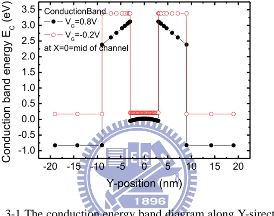
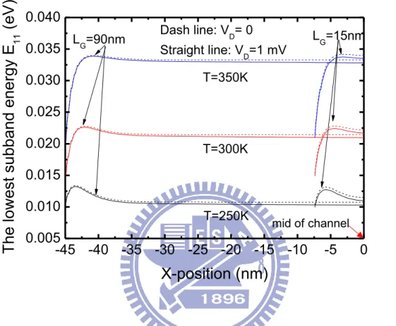
Usually we thought the highest energy of conduction band would locate at the mid of channel, but it would vary from the mid of channel toward the source and drain with increasing gate voltage. As shown in Fig. 3-3 is a profile of the lowest sub-band, E11, along the channel. We found the highest energy is located 2~5nm away from the junction of source/channel and channel/drain in channel. Fig. 3-4 show the sheet charge. In basic Poisson equation, we considered only forward or backward direction. In reality, we should take both into consideration. This leads to the result of Fig. 3-3. Apparently, the highest point of E11 is not located at the mid-channel. The difference between VD=0V and 1mV is due to the variation of Fermi-Level.
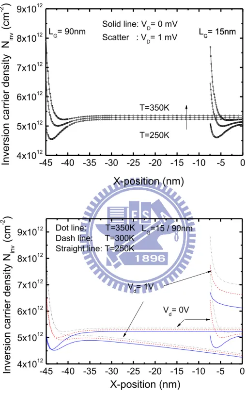
The local higher potential causes a relative lower carrier density at that region. As shown in Fig. 3-5 is the inversion carrier density Ninv along the channel. We get almost the same Ninv at VD=0V and 1mV. This shows channel is at equilibrium condition for VD=1mV. Furthermore, we find that the inversion carrier density can be gradually affected as the channel length is scaled down. The effect of drain induced barrier lowering, DIBL, can cause the carrier density increasing for LG=15nm, except at LG=90nm. It shows a similar characteristic as [13]. The short channel effect would appear for channel length is smaller than 40nm or the temperature of 150K.
13
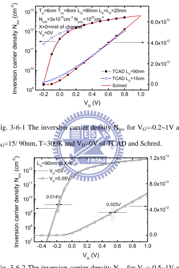
Finally, we want to compare how much difference between each channel length different gate voltages can produce. Here, we used a quite correct simulator, Schred [7], evaluated by Prof. Lundstrom, et al. at Purdue University, as the standard to check and analyze the TCAD’s simulation result. As shown in Fig. 3-6-1, we can get a perfect match between TCAD and Schred at long channel, but source and drain affect the channel as channel scaling to 15nm. Usually, we think DIBL is a constant for sub-threshold and above threshold region. Indeed, the channel resistance is high below the sub-threshold region; and above threshold region, the source and drain resistance are relative higher. Therefore, DIBL is not a constant for any gate voltage as shown in Fig. 3-6-2.
Section 3.2.3 Mobility Extraction at Equilibrium
After analyzing the status of channel at equilibrium, it provided two ways to calculate the mobility for us. First, according to the experimental concept, using the results of ID against VG and the inversion carrier density calculated by C-V measurement, we should assume that the drain current uniformly flows through the channel and the carrier uniformly distributes in channel. The results are shown in Eq. (3-8). Second, according to the ballistic theory, carriers come from the virtual source and may be reflected with a critical scattering length Lkt and a mean free path λ. Whatever the methods used, it should follow the DD model as Eq. (3-6) and (3-7). As shown in equation (3-8), we can get a relationship between ID per unit width and current density of electrons and holes. We can even reduce Eq. (3-8) to Eq. (3-9), because the majority carriers are electrons:
14
(3-8)
(3-9) Although the drain current is conserved along the channel, we can clearly find that from Fig. 3-5 the carrier density is not the same along the channel. From electron quasi Fermi-level along the channel as shown in Fig. 3-7, we can extract the series resistances of source and drain as shown in Fig. 3-8-1 and Fig. 3-8-2:
. (3-10) Fig. 3-8-1, 3-8-2 and 3-8-3 show Rtot, RSD and RChannel, respectively, for four different channel lengths from 90nm to 15nm and three temperatures. There is a slight difference between two applied VD, which is caused by the mobility degradation at VD=0.025V. That suggests that it is not appropriate to extract mobility at drain bias of 0.025V for nanoscale device. We could predict the trend of mobility by using the characteristic of the channel resistance that is proportional to 1/LG as revealed by Eq. (3-11). However, is not zero at LG=0nm at all for VD=0.025V: ; (3-11) , (3-12)
where is the apparent mobility, is the low field mobility, and is a correction term due to the mobility degradation.
15
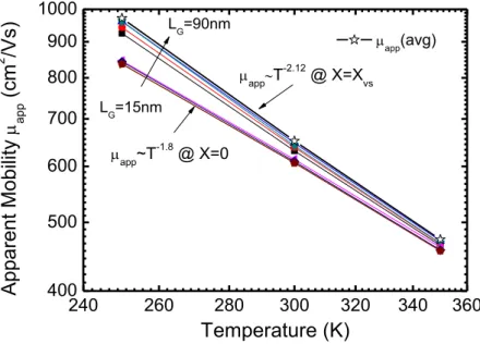
In Fig. 3-9-1, 3-9-2 and 3-9-3, we sight on the mid-channel (X=0) and X=Xvs. When VD is 1mV, there is no decrease on mobility with the channel length, but we can find a strong degradation on mobility at VD=25mV. This suggests the decrease of mobility with scaling down is caused by the saturation velocity. According to the Canali model evaluated by Canali et al. [4], it is used to explain the high field saturation phenomenon. The Caughey-Thomas formula is shown in below:
(3-13)
where is the saturation velocity and is a fitting parameter for Caughey-Thomas formula. Parameters’ setting is shown in Table 1. We confirmed the mobility degradation by using the Caughey-Thomas formula. As shown in Fig. 3-9-4, we set the low field mobility the same as the mobility extracted from DD model at VD=1mV and LG=90nm. The result agrees with our prediction. That is the mobility degradation caused by the limit of saturation velocity with channel length shrinkage.
Section 3.2.4 Critical Scattering Length LkT Extraction in Saturation
Region (VG=0.8V and VD=1V)
Within the framework of the channel backscattering theory, carrier will be scattered in the k-T layer. As the drain voltage is smaller than the thermal energy, the critical scattering length must be equal to the channel length. That explains why we should extract LkT in the saturation region.
16
LkT is expressed as:
(3-14) where and are taken as parameters that can fit the simulation result. Generally, we extract LkT from the conduction band energy profile . But would vary with x and y direction. Therefore, we used the lowest sub-band energy profile along the channel to substitute . As shown in Fig. 3-10-1, LkT increases with increasing channel length and increasing temperature. Fig. 3-10-2 shows the extracted LkT and the temperature coefficient for each channel length and temperature. It has the similar trend with Zilli, et al. [9]
Section 3.2.5 Injection velocity vinj Extraction in Saturation Region
(VG=0.8V and VD=1V)
Within the framework of the channel backscattering theory, carriers come from the virtual source. Therefore, the effective thermal injection velocity should be extracted at the source-channel barrier position [8].
(3-15) where was expressed as Eq. (3-2) and is the injection velocity for ith valley and jth subband:
(3-16)
where is the conductive effective mass for ith valley, is the density of state effective mass for ith valley, is the Fermi-level, is sub-band energy for ith valley and jth subband, and is the
17
Fermi-Dirac integral of order one-half. For two-fold valley, and for four-fold valley,
. Here the longitudinal mass =0.916 and the transverse mass =0.19 . The result has been shown in Fig. 3-11-1 and Fig. 3-11-2. It shows an increasing trend with temperature increasing and the temperature coefficient will increase with the channel length increasing.
Section 3.2.6 Inversion Carrier Density Ninv Extraction in Above
Threshold Region (VG=0.8 and VD=1mV/ 1V)
With channel length scaling down to nanoscale, an important question we faced is the short channel effects. The short channel effects are attributed to two physical phenomena: (i) the limitation of the drift characteristic; and (ii) the variation of the threshold voltage. Here, we focus on the phenomenon (ii). This is the variation of the carrier density with channel length scaling down for each temperature. As shown in Fig. 3-12-1 and Fig. 3-12-2, the applied drain voltage will cause the channel carrier density decreasing at LG=90nm and 45nm; and for LG=20nm and 15nm, the channel carrier density increases due to the DIBL effect. Therefore, the temperature coefficient of the inversion carrier density will vary with the channel length change. In the extraction of beta, there are two methods to do:
; (3-17)
(3-18) Furthermore, DIBL is not a constant for any gate voltage as shown
18
in Fig. 3-6-2. It complicates the status of channel with the varying applied gate voltage. Therefore, we focus on the above threshold region and use the maximum transconductance method to extract now. Result is shown in Fig. 3-12-4. Beta appears to slightly increase with channel length decreasing.
Section 3.2.7 Temperature Coefficient of Drain Current in Saturation Region (VG =0.8V and VD=1V)
The temperature coefficient of drain current α is the most important factor. It represents the combination of all the effects. Therefore, it should be the same as the result of the combination of each factor. Fig. 3-13-1 shows the same characteristic as Fig. 3-12-2.Here α can be expressed as:
(3-19)
. (3-20) The extracted result is shown in Fig. 3-13-3. We find α is smaller than α . This is because mobility has the higher value at low temperature. Therefore, in order to calculate the BR, α is the best way to extract the real variation of drain current between three temperatures. Owing to the same reason as α , is used to calculate the BR.
Section 3.2.8 Verification of Temperature Coefficient Method
Like the derivation shown in section 2.3, differentiating Eq. (3-9) with respect to temperature is performed:
. (3-21)
19
The result of each differential term has been shown in section 3-3, 3-6 and 3-7. At the saturation region, we assume the third of the right-hand side of Eq. (3-11) term is zero and
. Therefore, we can derive Eq. (3-22) as:
. (3-22) Result is shown in Fig. 3-14. It suggests that using the temperature coefficient method is feasible and the accuracy is better than 50%.
Section 3.3 Extraction of Ballistic Ratio (BR)
In this section, we will directly extract BR from the drain current and compare it with the temperature coefficient method. As shown in Eq. (3-23), we calculate BR at saturation region and there are two terms,
and , that should be calculated first:
(3-23) In the experiment part, we can measure C-V characteristics to get the corresponding inversion carrier density . Traditionally, the measured result is the macroscopic average. But in the channel backscattering theory it is not. It represents the carrier density at the barrier high in channel. Therefore, in the following we will extract BR at X=Xvs. As shown in Fig. 3-15-1, BR is extracted at the virtual source; it seems to increase with channel length shrinkage. This result shows the reflection rate decreasing with channel length decreasing. Considering the
20
physical limit on saturation velocity, it must saturate at : BR is about 0.75 and rc is about 0.15 at room temperature. Replacing BR with and Lkt, we have (3-24)
As shown in Fig. 3-15-2, λ is slightly larger than for higher temperature and BR increases with channel length shrinkage for the two methods. Although they have the same characteristics, the difference between each temperature is not the same. Therefore, we can predict BR extracted from temperature coefficient method. As shown in Eq. (2-16), we can use the five temperature coefficients to extract . Result is shown in Fig. 3-15-3 and it shows a nearly constant characteristic for each channel length. Furthermore, using the temperature coefficient set A assumed in [3] even shows a negative trend at LG=15nm/ 20nm. The reason is caused by the error in the five coefficients. In the five coefficients, we could simply assume the error would occur on critical scattering length. Other coefficients have been defined clearly. Therefore, substituting Eq. (3-24) into (3-23), we have
. (3-25)
The calculated critical scattering length is shown in Fig. 3-16-1. And according to the new , we can extract the new BR as shown in Fig. 3-16-2. As our anticipation, it shows similar characteristics as the result of direct calculation.
21
Chapter 4
Conclusion
In the study, we used TCAD simulator to predict the characteristic of DG nMOSFETs with channel length scaling down to nanoscale. Here, the most important issue is the high field velocity saturation. It causes the carrier mobility degradation for the even general applied measurement drain bias of 0.025V, and generates DIBL effect for channel length is smaller than 45nm. Therefore, we should measure the mobility at small enough drain bias like 1mV. But the mobility degradation effect still exists for the operation voltage. For this reason, Prof. Lundstrom, et al. at Purdue University brings up the channel backscattering theory. They used another concept to explain the velocity saturation effect. In the theory, they think the critical scattering length stems from the virtual source point to the point with kT potential drop, rather than the virtual source point. The result between the DD model and channel backscattering model has not too much difference. But as we used the temperature coefficient method to calculate BR, the slight difference in the critical scattering length causes a strong variation on the temperature coefficient LkT. We could infer carriers would be scattered in a range larger than kT-layer for higher temperature and in smaller than kT-layer for lower temperature. However, the channel backscattering theory is a useful theory to explain why we would face the awkward situation with the channel length scaling down.
22
References
[1] A. Pirovano, A. Lacaita and A. Spinelli, ―Two-dimensional quantum effects in nanoscale MOSFETs,‖ IEEE Trans. Electron Devices, vol. 49, no. 1, pp25-31, Jan. 2002.
[2] M. S. Lundstrom, ―Elementary scattering theory of the Si MOSFET,‖ IEEE
Electron Device Letters, vol. 18, no. 7, pp. 361-363, July 1997.
[3] M. J. Chen, H. T. Huang, K. C. Huang, P. N. Chen, C. S. Chang and C. H. Diaz, ―Temperature dependent channel backscattering coefficients in nanoscale MOSFETs,‖ in IEEE IEDM Tech. Dig., pp. 39-42, 2002.
[4]D. M. Caughey and R. E. Thomas, ―Carrier mobilities in Silicon empirically related to doping and field,‖ Proc. IEEE, pp. 2192–2193, Dec. 1967.
[5] M. J. Chen and L. F. Lu, ―A parabolic potential barrier-oriented compact model for the kbT layer’s width in Nano-MOSFETs,‖ IEEE Trans. Electron Devices, vol. 55, no. 5, pp. 1265-1268, May 2008.
[6] A. Rahman and M. S. Lundstrom, ―A compact scattering model for the nanoscale Double-Gate MOSFET,‖ IEEE Trans. Electron Devices, vol. 49, no. 3, pp. 481-489, March 2002.
[7] D. Vasileska, D. K. Schroder and D. K. Ferry, ―Scaled silicon MOSFET’s: Part II - Degradation of the total gate capacitance,‖ IEEE Trans. Electron Devices, vol. 44, no. 4, pp. 584-587, April 1997.
[8] F. Assad, Z. Ren, D. Vasileska, S. Datta and M. Lundstrom, ―On the performance limits for Si MOSFETs: a theoretical study,‖ IEEE Trans. Electron Devices, vol. 47, pp. 232-240, Jan. 2000.
[9] M.Zilli, P.Palestri, D.Esseni and L.Selmi, ―On the experimental determination of channel back-scattering in nanoMOSFETs,‖ in IEEE IEDM Tech. Dig., pp. 105-108,
23
2007.
[10] V. Barral, T. Poiroux, J. Saint-Martin, D. Munteanu, J. Autran and S. Deleonibus, ―Experimental investigation on the Quasi-ballistic transport: Part I—determination of a new backscattering coefficient extraction methodology,‖ IEEE Trans. Electron
Devices, vol. 56, no. 3, pp. 408-419, March 2009.
[11] V. Barral, T. Poiroux, D. Munteanu, J. Autran and S. Deleonibus, ―Experimental investigation on the Quasi-ballistic transport: Part II—backscattering coefficient extraction and link with the mobility,‖ IEEE Trans. Electron Devices, vol. 56, no. 3, pp. 420-430, March 2009.
[12] K. Natori, ―Ballistic metal-oxide-semiconductor field effect transistor,‖ J. Appl.
Phys., vol. 76, pp. 4879–4890, 1994.
[13] D. J. Frank, S. E. Laux and M. V. Fischetti, ―Monte Carlo simulation of a 30 nm Dual-Gate MOSFET: how short can Si go?,‖ in IEEE IEDM Tech. Dig., pp. 553-556, 1992.
[14] K. Banoo and M. S. Lundstrom, ―Electron transport in a model Si transitor,‖
24
25
Fig. 1-2 Schematic illustration of channel backscattering theory in terms of the conduction band profile. F+: the incident flux from the source is located at the peak of the source-channel barrier. Fb
-: the incident flux from the drain. T: the transmission coefficient for the flux cross the barrier for both directions.
26 -20 -15 -10 -5 0 5 10 15 20 -1.0 -0.5 0.0 0.5 1.0 1.5 2.0 2.5 3.0 3.5 C ond uction ba nd ene rgy E C ( eV ) Y-position (nm) ConductionBand VG=0.8V VG=-0.2V at X=0=mid of channel
Fig. 3-1 The conduction energy band diagram along Y-sirection.
T=300K, V
D=0V, V
G=-0.2V/ 0.8V and L
G=90nm.
27 -60 -50 -40 -30 -20 -10 0 10 20 30 40 50 60 -1.2 -1.0 -0.8 -0.6 -0.4 -0.2 0.0 At Y=0 VD=1V VG=0.8V C ond uction ba nd ene rg y E C ( eV ) X-position (nm) LG=90nm LG=45nm LG=20nm LG=15nm
Fig. 3-2 The conduction energy band diagram along the channel.
T=300K, V
D=1V, V
G=1V and L
G=15/ 20/ 45/ 90nm.
28 -45 -40 -35 -30 -25 -20 -15 -10 -5 0 0.005 0.010 0.015 0.020 0.025 0.030 0.035 0.040 LG=15nm LG=90nm T=250K T=300K T he low est su bba nd ene rgy E 11 ( eV ) X-position (nm) T=350K Dash line: VD= 0 Straight line: VD=1 mV mid of channel
Fig. 3-3 The lowest subband E
11along the channel. T=250/ 300/
350K, L
G=15/ 90nm and V
D=0/1mV. The difference between
29
30 -45 -40 -35 -30 -25 -20 -15 -10 -5 0 4x10¹² 5x10¹² 6x10¹² 7x10¹² 8x10¹² 9x10¹² LG= 90nm LLGG= 15nm= 15nm T=250K Inve rsion ca rr ier de nsity N inv ( cm -2 ) X-position (nm) T=350K Solid line: VD= 0 mV Scatter : VD= 1 mV -45 -40 -35 -30 -25 -20 -15 -10 -5 0 4x10¹² 5x10¹² 6x10¹² 7x10¹² 8x10¹² 9x10¹² Inve rsio n ca rr ier de nsity N inv ( cm -2 ) Vd= 1V Vd= 0V X-position (nm) Dot line: T=350K Dash line: T=300K Straight line: T=250K LG=15 / 90nm
Fig. 3-5 The inversion carrier density, N
invalong the channel.
T=250/ 300/ 350K, L
G=15/ 90nm and V
D=0/ 0.001/ 1V.
31 -0.2 0.0 0.2 0.4 0.6 0.8 1.0 109 1010 1011 1012 1013 0.0 2.0x10¹² 4.0x10¹² 6.0x10¹² Tsi=6nm Tox=6nm LG=90nm LS=LD=20nm Nsub=3x1016cm-3 Npoly=1020cm-3 X=0=mid of channel VD=0V Inve rsion ca rr ier de nsity N inv ( cm -2 ) VG (V) TCAD LG=90nm TCAD LG=15nm Schred
Fig. 3-6-1 The inversion carrier density N
invfor V
G=-0.2~1V at
L
G=15/ 90nm, T=300K and V
D=0V of TCAD and Schred.
Fig. 3-6-2 The inversion carrier density N
invfor V
G=-0.5~1V at
L
G=90nm, T=300K and V
D=0V/ 50mV.
-0.4 -0.2 0.0 0.2 0.4 0.6 0.8 1.0 107 108 109 1010 1011 1012 LG=90nm at X=0 VD=0V VD=0.05V Inve rsion ca rr ier de nsity N inv ( cm -2 ) VG (V) 0.025V 0.014V 0.0 4.0x10¹² 8.0x10¹² 1.2x101332 -60 -40 -20 0 20 40 60 0.0 0.2 0.4 0.6 0.8 1.0 E lectr on Qua si-F er mi le vel E f ( me V ) X-position (nm) LS=LD=20nm LG=15/20/45/90nm at Y=0 VD=1mV VG=0.8V T=250K T=300K T=350K
Fig.3-7 Electron Quasi-Fermi Level alone the channel for
L
G=15/ 20/ 45/ 90nm, V
D=1mV and V
G=0.8V at Y=0.
33 0 10 20 30 40 50 60 70 80 90 100 50 100 150 200 250 300 350 R to t = W V D /I D ( um )
Rtot Solid: VD=0.025V Open: VD=1mV
Square: T=350K Circle: T=300K Triangle: T=250K Line: Linear fitting
Channel Length (nm)
Fig.3-8-1 Total resistance for L
G=15/ 20/ 45/ 90nm at V
D=1mV/
25mV and V
G=0.8V.
0 10 20 30 40 50 60 70 80 90 100 50 55 60 65 70 75 80 RSD Solid: VD=0.025V Open: VD=1mVRtot @ LG=0nm Stright: VD=0.025V Dash: VD=1mV
Variation<1% Square: T=350K Circle: T=300K Triangle: T=250K R SD = W V SD /I D ( m) Channel Length (nm)
Fig.3-8-2 Source/ Drain resistance for L
G=15/ 20/ 45/ 90nm at
34 0 10 20 30 40 50 60 70 80 90 100 0 50 100 150 200 250 R C h a n n e l = W V C h a n n e l /I D ( m)
Rtot Solid: VD=25mV Open: VD=1mV
Square: T=350K Circle: T=300K Triangle: T=250K Line: Linear fitting
Channel Length (nm)
Fig.3-8-3 Channel resistance for L
G=15/ 20/ 45/ 90nm at
35 240 260 280 300 320 340 360 400 500 600 700 800 900 1000 appT-2.12 @ X=Xvs app(avg) app~T-1.8 @ X=0 A ppa rent M obility app ( cm 2 /V s) Temperature (K) LG=90nm LG=15nm
Fig. 3-9-1 The apparent mobility for L
G=15/ 20/ 45/ 90nm,
T=250/ 300/ 350K and V
D=1mV.
240 260 280 300 320 340 360 300 400 500 600 700 800 900 1000 A ppa rent M obility app ( cm 2 /V s) Solid: Qinv(0) LG=90nm LG=15nm Open: Qinv(Xvs) Temperature (K)Fig. 3-9-2 The apparent mobility for L
G=15/ 20/ 45/ 90nm,
36 260 280 300 320 340 360 300 400 500 600 700 800 900 1000 VD=1mV A ppa rent M obility app ( cm 2 /V s) Temperature (K) X=0 X=Xvs VD=25mV Dash line: X=0 Solid line: X=Xvs LG=15nm L G=90nm
Fig.3-9-3 The apparent mobility for L
G=15/ 20/ 45/ 90nm,
T=250/ 300/ 350K and V
D=1/ 25mV.
240 260 280 300 320 340 360 400 500 600 700 800 900 1000 A ppa rent M obility app ( cm 2 /V s) Temperature (K) X=Xvs VD=25mV LG=15nm LG=20nm LG=45nm LG=90nmSolid: extraction from DD model Open: calculation from CT model
VD=1mV
low is set app at VD=1mV and LG=90nm
Fig.3-9-4 The apparent mobility extracted from DD model and
calculated from CT model.
37
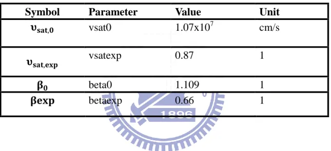
Table 1 Caughey-Thomas formula parameters
Symbol Parameter Value Unit
vsat0 1.07x107 cm/s
vsatexp 0.87 1
beta0 1.109 1
38 0 2 4 6 8 10 -40 -20 0 250K 300K Square: T=350K Circle: T=300K Triangle: T=250K VD=1V VG=0.8V T he low est su bba nd ene rgy E 11 ( me V ) X-XVS position (nm) LG=15nm LG=90nm 350K
Fig 3-10-1. Profile of the lowest subband energy E
11at V
G=0.8V
and V
D=1V.
200 400 600 800 1000 1 10 [9] Zilli, et al. Lg=15nm LkT=0.74 Lg=20nm LkT=0.87 Lg=50nm LkT=1.40 C ritical scatte ring le ngt h L kT ( nm ) Temperature (K) Lg=15nm LkT=1.609 Lg=20nm LkT=1.277 Lg=45nm LkT=1.585 Lg=90nm LkT=1.456Fig 3-10-2. kT-layer extension as a function of the temperature
at V
G=0.8V and V
D=1V.
39 1012 1013 1 1.1 1.2 1.3 1.4 1.5 Inject ion ve locity v inj ( 10 7 cm /s) Ninv (cm-2)
Cal: using Eij from Schred
T=250K T=300K T=350K
Fig 3-11-1. Injection velocity against the inversion carrier
density for three temperatures.
200 300 400 1 1.1 1.2 1.3 1.4 1.5 1.6 Inject ion V elocity v inj ( 10 7 cm/ s) Temperature (K) VG=0.8V VD=1V @X=Xvs LG=15nm Vinj=0.2933 LG=20nm Vinj=0.3143 LG=45nm Vinj=0.3366 LG=90nm Vinj=0.3346
[9] Zilli, et al. Ninv@Xvs=1013cm-2
LG=50nm Vinj=0.21
LG=20nm Vinj=0.17
Fig 3-11-2. Injection velocity as a function of the temperature at
V
G=0.8V and V
D=1V.
40 -1.0 -0.5 0.0 0.5 1.0 -1x10¹² 0 1x10¹² 2x10¹² 3x10¹² 4x10¹² 5x10¹² 6x10¹² 7x10¹² 8x10¹² Solid: LG=90nm Open: LG=45nm Center (+): LG=20nm Center (x): LG=15nm Inve rsion ca rr ier de nsity N inv ( cm -2 ) VG (V) Square: VD=1mV Circle: VD=1V T=250K
Fig 3-12-1. Inversion carrier density vs. V
G. At X=0 and
T=250K.
-0.5 0.0 0.5 1.0 106 107 108 109 1010 1011 1012 Solid: LG=90nm Open: LG=45nm Center (+): LG=20nm Center (x): LG=15nm Inve rsion ca rr ier de nsity N inv ( cm -2 ) VG (V) Square: VD=1mV Circle: VD=1V T=250KFig 3-12-2. Inversion carrier density vs. V
G. At X=0 and
41 -1.0 -0.8 -0.6 -0.4 -0.2 0.0 0.2 0.4 0.6 0.8 1.0 -1x10¹² 0 1x10¹² 2x10¹² 3x10¹² 4x10¹² 5x10¹² 6x10¹² 7x10¹² 8x10¹² 9x10¹² Solid: LG=90nm Open: LG=45nm Center (+): LG=20nm Center (x): LG=15nm Inve rsion ca rr ier de nsity N inv ( cm -2 ) VG (V) Square: T=250K Circle: T=350K VD=1V
Fig 3-12-3. Inversion carrier density vs. V
G. At X=0 and V
D=1V.
10 20 30 40 50 60 70 80 90 100 -0.5 0.0 0.5 1.0 1.5 2.0 2.5 3.0 e X=Xvs e X=0 th X=0 B eta ( 10 -3 K -1 ) Channel length (nm) [9] Zilli et al.
Fig 3-12-4. Beta for L
G=15/ 20/ 45/ 90nm, T=250/ 300/ 350K,
42 -0.6 -0.4 -0.2 0.0 0.2 0.4 0.6 0.8 1.0 1.2 10-5 10-4 10-3 10-2 10-1 100 101 102 103 104 LG=15nm LG=90nm LG=15nm LG=90nm VD=1V VD=1mV I D / W ( A/ m) VG (V) T=300K
Fig 3-13-1. Drain current vs. gate voltage.
10 20 30 40 50 60 70 80 90 100 -0.8 -0.6 -0.4 -0.2 0.0 0.2 T hr esho ld volta ge (V ) Channel Length (nm)
Solid: T=350K Open: T=300K Center: T=250K
VD=1V
VD=25mV
VD=1mV
gm,max method
Fig 3-13-2. V
th-L
G. V
thwas extracted by using the maximum
transconductance method.
43 10 20 30 40 50 60 70 80 90 100 -2.5 -2.0 -1.5 -1.0 -0.5 0.0 0.5 1.0 1.5 A lpha ( 10 -3 K -1 ) Channel Length (nm) th @ VD=1V th @ VD=25mV th @ VD=1mV ID @ VD=1V
44 10 20 30 40 50 60 70 80 90 100 0.5 1 1.5 2 e X=Xvs e X=0 th X=0
(
-
sate xp/ T ) /
Channel Length (nm)Fig 3-14. Ratio=
.
45 10 20 30 40 50 60 70 80 90 100 0.4 0.5 0.6 0.7 0.8 0.9 1.0 BR d ir = I D /Q inv (X vs )V inj = ( 1-r c )/( 1+ r c ) Channel Length (nm) VD=1V VG=0.8V T=350K T=300K T=250K Fig. 3-15-1 BR for LG=15/ 20/ 45/ 90nm, T=250/ 300/ 350K, VG=0.8
and VD=1V. BR increases with channel length scaling down.
10 20 30 40 50 60 70 80 90 100 0.4 0.5 0.6 0.7 0.8 0.9 1.0 BR = /( 2L kT + ) Channel Length (nm)
Solid: BRdir Open: BR
T=350K T=300K T=250K
Fig. 3-15-2 BR for LG=15/ 20/ 45/ 90nm, T=250/ 300/ 350K, VG=0.8
46 10 20 30 40 50 60 70 80 90 100 0.0 0.2 0.4 0.6 0.8 1.0 B R ( T C m ode l) Channel Length (nm)
Solid: BRdir Open: BR T=350K
T=300K T=250K
TC model set A [3]
Fig. 3-15-3 BR (TC model) calculation.
Set A [3]:
.47 240 260 280 300 320 340 360 0 5 10 15 L kT ca l ( nm ) Temperature (K) Solid: calculation Open: extraction LG=15nm LkT= 4.141 LG=20nm LkT= 3.578 LG=45nm LkT= 2.435 LG=90nm LkT= 2.234
Fig. 3-16-1 The calculated L
kTcalversus temperature for different
L
G, along with the extracted L
kT.
10 20 30 40 50 60 70 80 90 100 0.4 0.5 0.6 0.7 0.8 0.9 1.0 BR Channel Length (nm) BRdir T=350K T=300K T=250K BRTC LkTcal