國 立 交 通 大 學
電子工程學系 電子研究所碩士班
碩 士 論 文
具有加強轉換增益及雜訊相消機制
的 V-band 四倍頻器
A V-band Frequency Quadrupler with Spur
Cancellation and Conversion Gain Enhancement
研究生:任根生
指導教授:郭建男 教授
具有加強轉換增益及雜訊相消機制的
V-band 四倍頻器
A V-band Frequency Quadrupler with Spur Cancellation
and Conversion Gain Enhancement
研 究 生:任根生 Student:Gen-Sheng Ran
指導教授:郭建男 Advisor:Chien-Nan Kuo
國 立 交 通 大 學
電子工程學系 電子研究所碩士班
碩 士 論 文
A ThesisSubmitted to Department of Electronics of Engineering & Institute of Electronics College of Electrical Engineering and Computer Engineering
National Chiao Tung University In Partial Fulfillment of the Requirements
For the Degree of Master
In
Electronic Engineering Sept. 2011
Hsinchu, Taiwan, Republic of China 中 華 民 國 一百 年 九 月
I
具有加強轉換增益及雜訊相消機制的
V-band 四倍頻器
學生 : 任根生 指導教授 : 郭建男 教授
國立交通大學
電子工程學系 電子研究所碩士班
摘要
藉於操作在 V-band 頻段以達到高資料傳輸已是近來的趨勢,本論文主要是 設計一個低消耗功率的四倍頻器以做為在 V-band 系統下的應用,如做為升頻混 波器的本地震盪訊號等。此提出的四倍頻器為利用次諧波混合以增進其效能,包 含詳盡的非線性分析與實驗結果,證明其能更有效率產生四倍頻信號。 在本論文中實現的晶片是使用 TSMC 90-nm CMOS 製程,輸入端的中心操 作頻率為 12.5 GH,在 8 dBm 的基頻輸入功率下,輸出量得-20 dBm 的四倍頻訊 號(包含 3 dB 的四相位產生器損耗以及 9.5 dB 的輸出級損耗),功率消耗為 2.8mW,在輸出雜訊抑制上,基頻與二倍頻以及三倍頻諧波的抑制比分別是 53.5 dBc, 29.2 dBc 及 43 dBc,此外,在量測中也驗證我們提出的混頻架構可以在 同樣的功率消耗下,比直接利用四階非線性特性產生四倍頻要高出 4 到 7 dB 的 增益量。再者,整體直流功率消耗也控制在 3mW 以內,遠低於過去已提出的文獻。II
A V-band Frequency Quadrupler with Spur Cancellation
and Conversion Gain Enhancement
Student : Gen-Sheng Ran Advisor : Chien-Nan Kuo
Electronics College of Electrical Engineering and
Computer Engineering
National Chiao-Tung University
ABSTRACT
For the reason that the recent trend of high data-rate transmission operating at V-band, this thesis aims at the design of a low-power frequency quadrupler on the application of V-band system such as a local oscillator signal for the up-conversion mixer. Moreover, the frequency quadrupler we proposed is by use of sub-harmonic mixing to improve the efficacy. Through the nonlinear analysis in detail and experiment result, we can demonstrate a truth that the generation efficiency is enhanced.
The quadrupler circuit is designed and fabricated in TSMC 90nm CMOS technology. The input center frequency is 12.5 GHz. The measured output power level with an input signal of 8 dBm is -20 dBm( the date contains a loss of 3dB by differential-to-quadrature circuit and a loss of 9.5 dB due to the output buffer.), and the DC power consumption is 2.8mW. In respect of spurs rejection, the corresponding HRRs of f0. 2 f0, and 3 f0 are 53.5, 29.2, and 43 dBc, respectively. In addition, the
measure date also verify our proposed architecture get 4 to 7 dB higher than the merely direct generation from the forth-order derivative, which is in a fair comparison
III
of equal power consumption with each other. Moreover, the DC power consumption is merely 3mW, which is lower than prior works.
誌 謝
得以順利完成本篇論文,首先要感謝的是我的指導教授,郭建男教授,在郭 教授的竭力指導下學習到嚴謹的研究態度與具邏輯的分析方法,在此向老師致上 深深的敬意。 感謝鈞琳、明清、鴻源、俊興、子超、冠豪等學長們的不吝指導,在研究上 給予我許多的幫助與提供許多想法。也感謝和我一起做研究、一同奮鬥、互相勉 勵的佑偉、勁夫、敬修、馳光等同學們,以及暉舜、翰柏、品全、嘉佑、家愷、 威震、偉智和你們一起學習在我的碩士生活中留下許多難忘的回憶。感謝國家系 統晶片中心在晶片製作上所提供的協助。另外,感謝擔當口試評審委員的鍾世 忠、溫瓌岸教授給予的建議與指導,真的讓我獲益良多。 最後,要特別感謝我的父母與家人的栽培與鼓勵,因為你們相信我,我才能 一直走下去,以及其他親朋好友們的祝福,真誠感謝你們總是支持著我的決定。 任根生 一百年九月IV
CONTENTS
Abstract (Chinese)………..I
Abstract (English)……….II
Acknowledgements………..III
Contents………IV
Table Captions………VII
Figure Captions………VIII
Chapter 1 Introduction……….………1
1.1 Background and Motivation………...1
1.2 Thesis Organization………2
Chapter 2 Harmonic Generation by Nonlinear Behavior...3
2.1 Linearity and Nonlinearity………..3
2.2 Harmonic Generation….……….4
2.2.1 Single-frequency Excitation………...4
2.2.2 Two-frequency Excitation...………..………...7
2.3 Description of Nonlinearities in Analog Integrated Circuits…..9
2.3.1 Power Series Description of Basic Nonlinearities...10
2.3.2 Nonlinear Transconductance...10
2.3.3 Two-dimensional Transconductance...11
2.3.4 Three-dimensional Transconductance...12
2.3.5 Example: Drain Current of A MOS Transistor...13
V
Suppression...………..15
3.1 Introduction………..……….15
3.2 A Proposed Architecture of Frequency Quadrupler...19
3.3 Nonlinear Analysis of Sub-harmonic Mixing...21
3.3.1 First-Order Nonlinear Response...25
3.3.2 Second-Order Nonlinear Response...27
3.3.3 Third-Order Nonlinear Response...30
3.3.4 Forth-Order Nonlinear Response...31
3.3.5 Computing...32
3.4 Design for the Frequency Quadrupler...35
3.4.1 A Method to Analyze Sub-harmonic Mixing...35
3.4.2 Design for the Frequency Quadrupler...38
3.4.3 Quadrature All-pass Filter(QAF)...46
3.4.4 Output Buffer...49
Chapter 4 Chip Implement and Measurement Result...50
4.1 Measurement Setup... ...50
4.2 Measurement ... ...50
4.2.1 Sensitivity of Phase Mismatch...50
4.2.2 Output Harmonic Response...52
4.2.3 The Verification of the Enhancement by Sub-harmonic Mixing...55
4.2.4 Phase Noise...58
4.3 Comparison with Published Works...60
Chapter 5 Conclusion and Future Work...61
VI
5.2 Future work...61
References……….63
Vita………66
VII
TABLE CAPTIONS
Table 2.1 Definition of the nonlinearity coefficients of the drain current of a nMOS transistor...14 Table 4.1 The measurement dates before and after laser cut...57 Table 4.2 Summaries and Comparison with Published Works...60
VIII
FIGURE CAPTIONS
Figure 2.1 The differential harmonics at the output of an analog circuit excited by a
sinusoidal signal at frequency 1...5
Figure 2.2 The different frequency components at the output of a weakly nonlinear circuit with the input-output relationship given by equation (2.1) to a combination of two sinusoidal signals with the same amplitude A...8
Figure 3.1 The quadrupler circuit schematic of reference[1]...16
Figure 3.2 Measurement date of reference[1]...16
Figure 3.3 Stacked quadrupler of reference[3]...17
Figure 3.4 Quadrupler schematic of reference[2]...18
Figure 3.5 A typical quadrupler by way of direct generation...20
Figure 3.6 The architecture of proposed quadrupler...21
Figure 3.7 The concept of circuit implementation of the proposed quadripler...21
Figure 3.8 The sub-harmonic mixer, which is the half circuit of the proposed quadrupler with the differential-pair topology...23
Figure 3.9 The equivalent circuit for nonlinear analysis...23
Figure 3.10 The equivalent circuit for the analysis of second-order response...27
Figure 3.11 The circuit of sub-harmonic mixer for nonlinear analysis...32
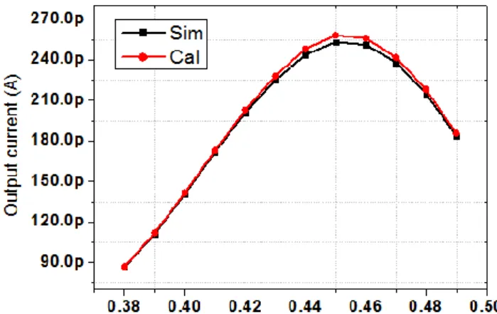
Figure 3.12 The comparison of calculation and simulation results for the output current at 4f0...33
Figure 3.13 The comparison of calculation and simulation results for the output current at 4f0 with alpha increasing from 0 to 1%...34
Figure 3.14 The calculation result of 4f0 and three components separately...34
IX
nonlinear analysis of sub-harmonic mixer...36
Figure 3.16 The alteration between the actual and the approximate condition for the nonlinear analysis of sub-harmonic mixer...37
Figure 3.17 The half circuit of the proposed quadrupler...38
Figure 3.18 The practical topology of current sink which combine bias current and injection current...39
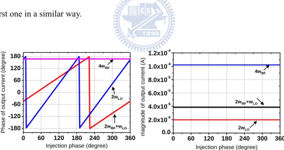
Figure 3.19 The simulation result for injection phase to the output components of 4f0, with a fix alpha of 0.5...40
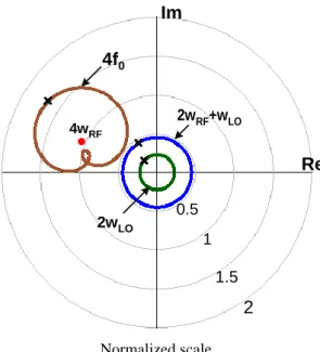
Figure 3.20 Re-draw the figure 3.19 in polar plot, the cross mark the location where the injection phase is 180 degree...41
Figure 3.21 Full schematic of the proposed quadrupler with each phase condition of input. ...41
Figure 3.22 Simulation shows the larger , the more mixing as well as the more 4f0...44
Figure 3.23 The simulation of according to VGS of the doubler...43
Figure 3.24 The half of the proposed quadrupler with definition of two stages...43
Figure 3.25 Simulation results of the half circuit according to the bias and size selection of the doubler stage...44
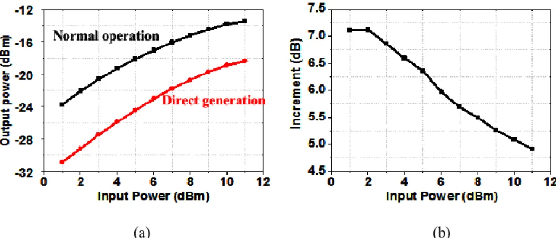
Figure 3.26 (a) The comparison of normal operation and direct generation. (b) The increment by sub-harmonic mixing...44
Figure 3.27 The 4f0 and each contribution in polar plot...45
Figure 3.28 The sensitivity of bias voltage at the operation point...46
Figure 3.29 The mechanism of QAF from the paper... 47
Figure 3.30 Express the OAF in polar plot...48
Figure 3.31 (a) The magnitude unbalance by large loading effect. (b) Melioration by adding a resistor RD...48
X
Figure 4.1 The die micrograph of chip implement...51
Figure 4.2 The measurement setup for V-band...51
Figure 4.3 Output harmonics variation due to the mismatch of input phase ...52
Figure 4.4 (a) The frequency response of output harmonics with 8 dBm input power. (b) the corresponding HRRs of (a)...53
Figure 4.5 (a) The power transfer function of harmonics at input frequency 12.5 GHz. (b) the corresponding HRRs of (a)...53
Figure 4.6 The frequency responses with varied input power level of 0, 4 ,and 8 dBm respectively. (a) Output power. (b) HRR1. (c) HRR2. (d) HRR3...54
Figure 4.7 The photograph of output spectrum under the condition that fundamental frequency is 12.5GHz with 8 dBm input power...54
Figure 4.8 Individual output spectrum of figure 4.7 with the span of 1MHz (a) f0 (12.5GHz). (b) 2 f0 (25GHz). (c) 3 f0 (37.5GHz). (d) 4 f0 (50GHz)...55
Figure 4.9 The location of laser cut in the circuit, we disconnect the signal paths of doubler stage but keep the voltage bias paths intact...56
Figure 4.10 The location of laser cut in the chip...56
Figure 4.11 (a) The output power of two conditions. (b) The increment...58
Figure 4.12 The comparison of figure 3.26(b) with figure 4.11(b)...58
Figure 4.13 The measured phase noise of the input and output signal...59
1
Chapter 1
Introduction
1.1 Background and Motivation
Owing to the advances of wireless communication systems, the operation frequency moves from radio-frequency up to millimeter-wave. The development of millimeter-wave front-end has been prospering in recent research. In general, high-frequency circuits usually need devices with better properties such as SiGe BiCMOS technology. Now utilizing a low-cost and advanced CMOS process is a trend for the integration. Therefore, the circuit we proposed is implemented and fabricatd in tsmc 90-nm CMOS process provided by CIC. A frequency quadrupler with spurs rejection on V-band application such as a local oscillator signal has been designed mainly in this thesis.
Frequency multipliers are widely employed in communication system for providing high frequency signal from a low-noise and low-frequency oscillator. A frequency quadrupler with a frequency multiplication ratio of four is more difficult to realize because the four-order harmonic at 4 f0 is far from the fundamental frequency
and the nonlinear intermodulation product at this frequency is usually lower compared to those at 2 f0, and 3 f0. Existing frequency quadrupler are square-wave generators
that have filtered output to select the forth-order harmonic at 4 f0[1][2], this results in
poor efficiency since most power is wasted in the undesired terms. For example, in reference[1], The concept is just through driving the strongly non-linear devices to get nonlinear harmonics then filtering out the undesired harmonics. Furthermore, a weak point is its poor spur harmonics rejection because of low quality of output filter
2
operating at high frequency, especially the spurs around the desired harmonic. Therefore, to achieve the further suppression of spur harmonics inevitably need additional filters.
In conclusion, we try to explore some great technique to efficiently generate this fourfold frequency, and then a method of exploiting the sub-harmonic mixing to enhance generation efficiency is proposed and analyzed. Besides, it shows great reduction in circuit complexity compared with other published works.
1.2 Thesis Organization
In Chapter 2, fundamentals about nonlinear circuit are introduced. Techniques and principles relating to the analysis of nonlinear system are also mentioned.
In Chapter 3, the detailed design and analysis of a frquency quadrupler with spurs rejection is described. We also introduce the Volterra series to analyze the nonlinear behavior.
In Chapter 4, chip implement and measurement result is demonstrated including harmonic response, phase noise, and the verification of efficacy by sub-harmonic mixing.
3
Chapter 2
Harmonic Generation by Nonlinear Behavior
2.1 Linearity and Nonlinearity
A fundamental truth of electronic engineering is all electronic circuits are nonlinear. Generally, the linear assumption that underlies most modern circuit theory is practically nearly an approximation. Some circuits, such as small-signal amplifiers, are very weakly nonlinear, and are usually be regarded as linear in systems. However, in these circuits, nonlinear behavior are often crucial factors that degrade system performance and must be minimized. As to some circuits, such as frequency multipliers, exploit the nonlinearities in their circuit elements; these circuits would be hardly implement if nonlinearities did not exist. So the courses of these circuits are often desirable to maximize the effect of the nonlinearities, and even to maximize the effects of annoying linear phenomena. The difficulty of analyzing and designing such circuits is usually more severe than for linear circuits; it is the main subject.
Linear circuits are defined as those which can put the superposition principle into analyzing. Specifically, if excitations x1 and x2 are applied separately to a circuit
having responses y1 and y2, respectively, the response to the excitation ax1+bx2 is
ay1+by2, where a and b are arbitrary constants. This criterion can be applied to either
circuits or systems. This definition implies that the response of a linear, time-invariant circuit of system includes only those frequencies present in the excitation waveforms. Thus, linear, time-invariant circuits do not generate new frequencies. As nonlinear circuits usually generate a remarkably large number of new frequency components, this criterion provides an important dividing line between linear and nonlinear
4
circuits.
Nonlinear circuits are often characterized as either strongly nonlinear or weakly nonlinear. Although these terms have no precise definitions, a good working distinction is that a weakly nonlinear circuit can be described with adequate accuracy by a Taylor series expansion of its nonlinear current/voltage (I/V), charge/voltage (C/V), or flux/current (Φ/I) characteristic around some bias current or voltage. This definition implies that the characteristic is continuous, has continuous derivatives, and for most practical purposes, does not require more than a few terms in its Taylor series. Virtually all transistors and passive components satisfy this definition if the excitation voltages are well within the component’s normal operating ranges; that is, below saturation.
2.2 Harmonic Generation
2.2.1 Single-frequency Excitation
We will first describe the frequency spectrum at the output of the test circuit when it is excited with one sinusoidal source at a frequency 1. When the amplitude
A1 of the input signal is small enough, then the output spectrum of the circuit only
contain one frequency component above the noise floor, this is to say, the response corresponding to the circuit's linear behavior. This is a signal at the same frequency of the input signal, called the fundamental frequency. The amplitude of this signal change proportionally with the input amplitude.
When the input amplitude increased, the output spectrum contains signals at the frequencies 21 and 31, and these signals called the second and third harmonics,
originate from second- and third-order nonlinear circuit behavior. Respectively, as we shall see below. Harmonics higher than the third, caused by higher-order behavior,
5
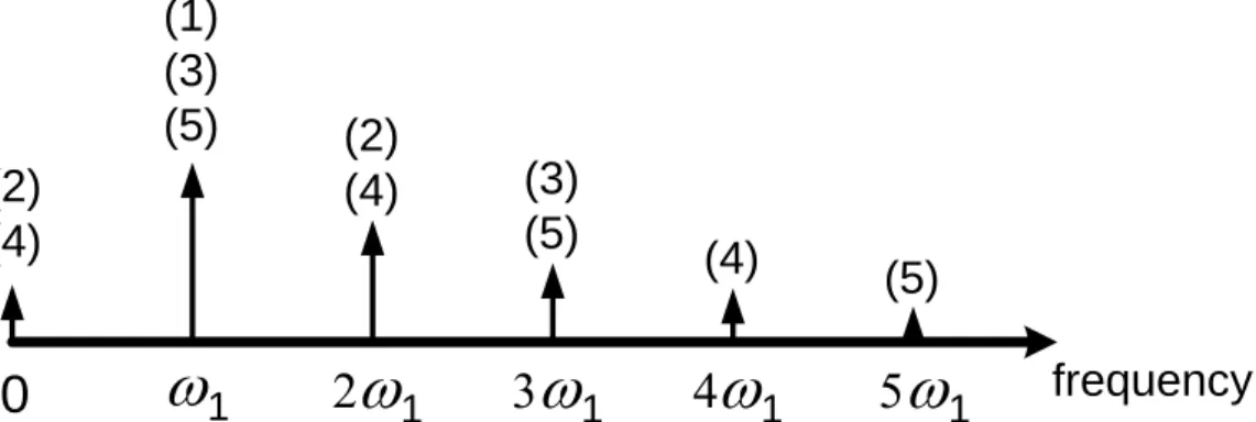
come above the noise floor at even higher input amplitudes. It is seen that the amplitude of the nth harmonic increases with the nth power of the input amplitude: an increase of the input amplitude with 6dB yields an increase of the second harmonic at the output with 12dB, the third harmonic increases with 18dB and so on. At high input amplitudes, this is not true anymore. Then it is observed that the third-order nonlinear behavior also give rise to a component at the fundamental frequency which increases with the third power of the input amplitude. As a result, the fundamental response can increase faster than linear, which for an amplifier means that the gain slightly increase. In this case one speak about gain expansion. On the other hand, if the increase is less than linear because the sign of the third-order contribution is opposite to the sign of the linear response, then a gain compression is observed in the output. Similarly, forth-order behavior gives a contribution to the second harmonic and so on. This situation is depicted in Figure 2.1. Signals caused by nonlinear behavior of order higher than five are not shown in this figure. Also it must be noted that a component at 0Hz is found at the output. This DC shift is caused by second-order, forth-order, or in general, even-order nonlinear behavior.
10
1
1
1
1(2)
(4)
(1)
(3)
(5)
(2)
(4)
(3)
(5)
(4)
(5)
frequency
Figure 2.1 The differential harmonics at the output of an analog circuit excited by a sinusoidal signal at frequency 1. The numbers between brackets indicate the order of nonlinear behavior
6
The nonlinear behavior as discussed above in a qualitative way can be clarified mathematically with a simple example. Assume that the relationship between the input signal x(t) (which is either a current or a voltage) of a circuit and the output y(t) is given by the following relationship
y t( )K x t1
K2
x t
2K3
x t
3... (2.1)When the input-output relationship is given explicitly by an analytic relationship y t
f
x t
(2.2) Then the coefficients K1,K2,K3,... can be identified with the coefficients of a Taylorseries of f : 1 df K dx (2.3) 2 2 2 1 2 d f K dx (2.4) 3 3 3 1 6 d f K dx (2.5) The coefficient K1 describes the behavior of the linearized circuit. This behavior is
often referred to as first-order behavior. The coefficients K2,K3,... are called
second-order and third-order nonlinearity coefficients, respectively, in general, high-order nonlinearity coefficients.
Returning to our example, we assure that the input signal x(t) has the form x t
Acos
1t1
(2.6)Substituting this expression into equation (2.4) yields the output y(t) :
2
1 1 1 2 1 1 1 1 cos cos 2 2 2 2 y t AK t A K t 3 3 3cos
1
1 1cos 3
1 3
1 4 4 A K t t (2.7)It is seen that the second-order coefficient K2 give rise to a signal at 21 and at
7
Therefore, these signals are denoted as second-order signals. And the third-order signals at the frequency 31 and at the fundamental frequency 1 are with the same
reason. Assure K3 has the same sign as K1, in this case the third-order signal at the
fundamental frequency as the same sign at the first-order signal. In other words, the amplitude of the fundamental signal has increased due to third-order behavior. This situation corresponds to expansion. If K1 and K3 have an opposite sign then we have
compression.
2.2.1 Two-frequency Excitation
In the same way as in the previous section, the test circuit under consideration is now excited with two sinusoids A1cos(1t) and A2cos(2t), both applied at the same
input port. When A1 and A2 are sufficiently low, the output spectrum contains two
signals above the noise floor at the fundamental frequency 1 and 2 due to the
circuit's linear behavior. Because in a linear circuit the superposition principle is valid, the two excitations don't produce any interfering signal. However, When A1 and A2
become larger, then, apart from the harmonics of 1 and 2, interfering signals grow
above the noise floor at the frequency 1+2, ∣1-2∣, 21+2, ∣21-2∣,
1+22 and ∣-1+22∣. The signals at ∣1±2∣are caused by second-order
nonlinear behavior and are called second-order intermodulation products. They increase with the first power of both A1 and A2. The other signals come from
third-order behavior and are denoted as third-order intermodulation products. The signals at ∣1±2∣increase with the square of A1 and with the first power of A2,
and so on.
For analog circuits such as amplifiers, the intermodulation products are usually unwanted. Therefore, they are denoted as intermodulation distortion. In communication circuits, these unwanted products are often denoted as spurious responses. Then consider again the test circuit with the input-output relationship given
8
by equation (2.1). When the input signal x(t) consists of two signals of equal amplitude and with a different frequency 1 and 2:
x t
Acos
1t Acos
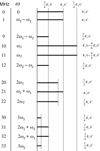
2t (2.8) Then the different responses are shown in Figure 2.2. It is assumed that the amplitude A is sufficiently low such that the circuit behaves in a weakly nonlinear way. The frequency w1 and w2 are have been given the value *10 MHz and *11 MHz. It is seen that harmonics of 1 and 2 are present at the output as well as intermodulationproducts. MHz
0 0 1 9 1 –2 2 –1 10 1 2 2 K A 2 2 K A 2 2 K A 3 3 3 4K A 3 3 3 4K A 3 1 3 9 4 K A K A 3 1 3 9 4 K A K A 11 2 12 2 –1 3 3 3 4K A 20 21 22 1 2 + 1 2 2 2 1 2K A 2 2 1 2K A 2 2 K A 30 31 32 33 1 2 2 + 1 1 + 2 3 3 1 4K A 3 3 1 4K A 3 3 3 4K A 3 3 3 4K A 3 3 1 4K AFigure 2.2: The different frequency components at the output of a weakly nonlinear circuit with the input-output relationship given by equation (2.1) to a combination of two sinusoidal signals with the same amplitude A. The frequency of the two input signals are 10 MHz and 11 MHz.
9
2.3 Description of Nonlinearities in
Analog Integrated Circuits
prior to the analysis of nonlinear behavior of analog circuits, it is necessary to describe the nonlinear devices that are present in analog circuits. The devices most commonly used in silicon analog integrated circuits are transistors, resistors, capacitors and diodes. In circuit analysis the devices mentioned above are described using an equivalent circuit. This equivalent circuit can be as simple as one circuit element (e.g. one resistor), or it consist of several circuit elements (e.g. transistor). The elements of such equivalent circuit are nonlinear in general. The following circuit elements are used in analog integrated circuits as a part of the equivalent circuit of a device.
▬ A nonlinear conductance: the current through this element is an algebraic function of the voltage over the element.
▬ A nonlinear transconductance: the current through this element is an algebraic function of a voltage other than the voltage over the element.
▬ A nonlinear resistance: the voltage over this element is an algebraic function of the current through this element.
▬ A nonlinear transresistance: the voltage over this element is an algebraic function of a current different from the current through this element.
▬ A nonlinear capacitance: the charge on this element is an algebraic function of the voltage across the element.
▬ A nonlinear transcapacitance: the charge on this element is an algebraic function of the voltage across the element.
These circuit elements are referred to as basic nonlinearities, since they are the building elements for nonlinear equivalent circuits of devices such as transistor,
10
diodes, integrated resistors,... Nonlinear voltage-controlled voltage sources and current-controlled current sources are seldom used in equivalent circuits of devices in analog integrated circuits.
2.3.1 Power Series Description of Basic Nonlinearities
A power series description of a basic nonlinearity contains the derivatives of the output quantity (current or voltage) with respect to the controlling quantities. These derivatives are evaluated in the quiescent point. An accurate description of a nonlinear device in terms of power series requires that the different derivatives that are considered be accurate. These derivatives are a function of the controlling quantities and of the model parameters that describe the nonlinear device. The main nonlinearities in transistor are transconductances, then we look into the derivation of the nonlinear coefficients as following sections.
2.3.2 Nonlinear Transconductance
For a nonlinear transconductance, the current through the element iOUT(t), is a
nonlinear function f of the controlling voltage vC(t) elsewhere in the circuit. This
function can be expanded into a power series around the quiescent point IOUT = f(VC):
iO U T
t f
v
C
t
f VC
cv
t
1 1 ! C k k C k c k v V f v t f V v t k v
(2.9)In this equation iOUT(t) is the total value of the current, which is the sum of the DC
and the AC current. The voltage vc(t) is the AC voltage that controls the conductance.
The second term in equation (2.9) is a power series representing the AC part of the current. When the analysis of a circuit that contains a nonlinear conductance is limited to first- second- and third-order nonlinear behavior, then the power series in equation
11
(2.9) can be broken down after the third term. Defining the following coefficients
1
C v V f v g v (2.10)
1 2 2, 2 1 2! C g v V f v K v (2.11)
1 3 3, 3 1 3! C g v V f v K v (2.12)In which we omitted the time dependence for simplicity, and in general
1 , 1 ! C n n g n v V f v K n v (2.13)Leads to the expression of the AC current through the conductance
1 1 2 3 1 2, 3, ... OUT c g c g c i t g v t K v t K v t (2.14) In this expression, g1 is the small-signal transconductance of the linearized circuit.The coefficients in the second and third term, K2,g1 and K3,g1 are respectively the
second- and third-order nonlinearity coefficients that describe the nonlinear element. Similarly, the small-signal conductance is often referred to as the first-order
coefficient. The subscript for K2 and K3 is the symbol that represents the linearized
element, in this case g1.
2.3.3 Two-dimensional Transconductance
A two-dimensional transconductance is an element the current of which is controlled by two different voltage. In other words, the current iOUT(t) is a function f of two
voltages uC and vC, which can be expressed in terms of AC values using a
12 iOUT
t f u
C
t ,vC t
f U
C u t Vc
, Cv tc
1 0 , , ! ! C C m n m n c c C C n m n u U m n v V f u v u t v t f U V u v n m n
(2.15)The AC part of the current corresponds to the second term of equation(2.15), which is a two-dimensional power series. This series can be split into three series i1, i2 and i3,
each corresponding to a part of the total AC current. 1 1 2 3 1 1 c 2,g c 3,g c ... i g u K u K u (2.16) 2 2 2 3 2 2 c 2,g c 3,g c ... i g v K v K v (2.17) The time dependence of uc and vc has been omitted for simplicity. The third series, i3,
contains nothing but cross-terms, which are terms that contain a nonzero power of both uc and vc.
1 2 1 2 1 2
2 2
3 2,g&g c c 3,2g&g c c 3,g&2g c c
i K u v K u v K u v (2.18) The meaning of the subscripts in the nonlinearity coefficients defined above is as
follows. Suppose that the first-order derivative of the total current with respect to u and v are respectively g1 and g2. Then a coefficient like Km,jg1&(m-j)g2 with m and j
positive integers and m > j means
1 2 , & , 1 1 ! ! m m jg m j g j m j f u v K u v j m j (2.19) 2.3.4 Three-dimensional TransconductanceA three-dimensional transconductance is a current source that is controlled by three voltage. In other words, the current is a function f of three voltage u(t), v(t), and w(t). Using a power series expansion around the quiescent value of the current can be split into a quiescent part IOUT = f(UC,VC,WC) and an AC part. This AC part is given by
13 iOUT
t f U V W
C, C, C
1 0 0 , , ! ! ( )! C C C k i j k i j k k i c c c i j k i j u U k i j v V w W f u v w u t v t w t u v w i j k i j
(2.20)The AC current can be split into distinct parts, and this series implies the introduction of the following nonlinearity coefficients.
1 2 3 , & & ( ) , , 1 1 1 ! ! ! m m jg kg m j k g j k m j k f u v w K u v w j k m j k (2.21)2.3.5 Example: Drain Current of A MOS Transistor
The meaning of the newly defined coefficients is illustrated with a simple model for the drain current of an nMOS transistor in saturation. Taking into account bulk effect and Early effect, the drain current is given by
2 1
2 P D G S T D S K W i v V v L (2.22) with VT VT O
vS B
(2.23) The parameter, , and are the channel-length modulation factor, the body-effectcoefficient and the surface inversion potential, respectively. The first derivatives of the current with respect to the controlling voltage vGS, vBS, and vDS are the
small-signal parameters gm, gmb, go. Then from above equations the AC current is
14 2 3 2, 3, 2 3 2, 3, 2 3 2, 3, 2 2
2, & 3,2 & 3, &2 2 2, & 3,2 & ... ... ... ... m m o o mb mb m mb m mb m mb m o m o d m gs g gs g gs o ds g ds g ds mb bs g bs g bs g g gs bs g g gs bs g g gs bs g g gs ds g g gs i g v K v K v g v K v K v g v K v K v K v v K v v K v v K v v K v v 2 3, &2 2 2
2, & 3,2 & 3, &2 3, & & ... ... ... m o mb o mb o mb o m mb o ds g g gs ds g g bs ds g g bs ds g g sb ds g g g gs bs ds K v v K v v K v v K v v K v v v (2.24)
In this equation, the first three line correspond to series that describe the dependence of the AC drain current on one single AC voltage. The following three lines represent the variation of the current when two voltages change at the same time. The last line describes the variation of the current with the three controlling voltages at the same of the three-dimensional drain current in general requires sixteen second- and third- order coefficients. Table 2.1 lists the expressions for the coefficients that describe the nonlinearity of the drain current according to equation 2.24, and only shows coefficients with respect to gm.
m g 2,gm K 3, m g K 2, & m mb g g K 2, & m mo g g K D GS i v 2 2 1 2 D GS i v 3 3 1 6 D GS i v 2 D GS BS i v v 2 D GS DS i v v 3,gm&2gmb K 3, &2 m o g g K 3,2 & m mb g g K 3,2 & m o g g K 3, & & m mb o g g g K 3 2 1 2 D GS BS i v v 3 2 1 2 D GS DS i v v 3 2 1 2 D GS BS i v v 3 2 1 2 D GS DS i v v 3 1 6 D GS BS DS i v v v
Table 2.1 Definition of the nonlinearity coefficients of the drain current of a nMOS transistor.
15
Chapter 3
A Frequency Quadrupler with Spur Harmonics
Suppression
3.1 Introduction
Active frequency multipliers are utilized in numerous applications to efficiently provide a source of high frequency microwave energy. They are commonly used in communication systems to enable frequency translation of a signal from a low-noise and low-frequency oscillator to the required higher frequency band for the purpose of up/down conversion in transceivers.
In general, frequency quadrupler and higher order multipliers have not seen more prominence and detailed investigation than doublers and triplers, due to higher circuit complexity and lower achievable conversion gain and efficiency. Therefore, at first we inspect some published works about quadrupler.
Begin with the work pronounced by professor Huei Wang, proceedings of 2010
EuMC conference[1]. The circuit schematic is shown in figure 3.1. A single-stage
V-band frequency quadrupler is proposed and manufactured in 0.25-μm SiGe BiCMOS technology. The maxima output power is -10 dBm with 11.7 mW dc power consumption. The concept is through driving the strongly non-linear devices to get nonlinear harmonics then filtering out the undesired harmonics. The conversion efficiency is poor by this approach. Another weak point is its poor spur-harmonic rejection of output signal because of low quality of output filter operating at high frequency, especially the spurs around the desired harmonic. In the design of frequency quadrupler, the third-order spur harmonic at frequency 3f0 is in particular
16
hard to suppress. The measured dates shown in figure 3.2 clearly shows the poor harmonic rejection, especially the spur at 3f0. Therefore, to achieve the further
suppression of spur harmonics inevitably need additional filters. It is an inconvenient concern. According to the paper, the merit of the circuit is the 36% bandwidth from 52 to 75 GHz. In my opinion, it takes advantages of the strongly non-linear devices of SiGe BiCMOS technology, and by large input signal to make the output power achieve the saturation point in the frequency band.
Next, the work pronounced by Infineon Technologies AG, proceedings of 2009
EuMIC conference[3]. This work is manufactured in a Silicon-Germanium production
Figure 3.1 The quadrupler circuit schematic of reference[1].
17
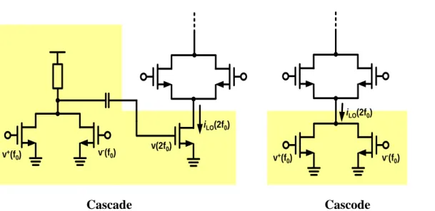
technology, and the schematic is shown in figure 3.3. The DC consumption of this quadrupler is 43mW from 3.5 V supply voltage and RF output power is -5dBm at frequency 77GHz. From my point of view, it is a good work. The structure is using two doublers stacked one by one. Therefore, the cost is higher supply voltage for stacking, and the requirement of quadrature input signal for each Gibert mixer operation. So the circuit contains several TRLs for 90 degree phase shifting which increases the complexity of design and chip area, especially when operating in lower frequency application.
Next, the work pronounced by professor Euisik Yoon, proceedings of 2005
TMTT[2]. The schematic shown in figure 3.4 is manufactured in a 0.18- m CMOS process. The DC consumption of the quadrupler is 106mW with 1.8V VDD and it has -18 dBm RF output power at frequency 40 GHz. Apparently, the focal point of this paper is not with an emphasis on the quadrupler. It merely contains four transistors biased at the maxima forth-order derivative of transconductance. The disadvantages
18
are high power consumption and low conversion efficiency. Although the design do not have any particularity, except for the linear superposition. It let us think of some possibilities that can upgrade the circuit.
Finally, in this work, a new technique of generating the forth-order harmonic at 4f0
is proposed and analyzed. It improves the generating efficiency by not only direct generation, but also mixing generation. Applying this technique, frequency 4f0 can be
generated under low power consumption and the circuit itself is uncomplicated compared with other published methods. Analytical equations were developed to approximate the numerically-converged results of CAD tools for optimization with paper and hand calculation. Detailed analyses were done to maximize the frequency 4f0 and suppress the undesired harmonics. According to the experimental results, the
output power of proposed quadrupler is -20dBm (contained 9.5 dB loss of the output buffer) under only 4.5 mW dynamic power consumption with fundamental input power of +8 dBm. The proposed quadrupler is fabricated using TSMC 90-nm
low-leakage CMOS technology for the verification of theoretical results. Figure 3.4 Quadrupler schematic of reference[2].
19
In Section 3.2, the architecture of the proposed quadrupler is introduced preliminarily. The nonlinear analysis by Voterra series are presented in Section 3.3. The design procedure of the proposed quadrupler is illustrated in Section 3.4, including the design of quadrature all pass filter.
3.2 A Proposed Architecture of Frequency Quadrupler
In the last section we saw several types of methods to devise a quadrupler. Principally, you can find some issues which dominate the performances such as power consumption, harmonic rejection ratio(HRR), and conversion gain...etc. But however, a technique which can advance the performance in all aspects is nearly impossible. When a technique can improve some quality, a drawback maybe emerges at the same time. Consequently, ameliorating the drawback is the target for all designers. Return to the topic, in the beginning we should determine what features are our desires. Apart from low power consumption being a trend, perfect HRR is a significant criterion for multipliers. Because a multiplier with perfect HRR can avoid connecting superfluous filters after the output, especially when operating at high frequency. We have studied several examples of the quadruplers, and the best way to eliminate the spur harmonics is by cancellation instead of oppression. Some methods similar to filtering have difficulties handling the spurs adjacent to the desired harmonic. For the quadrupler the spur harmonics at 3f0 and 5f0 are hardly suppressed by filtering. But cancellation can
thoroughly eliminate spurs. Consequently, to accomplice lower power consumption and great HRR, we take sub-harmonic mixers and quadrature input signals as the first step and the circuit is shown in figure 3.5; as we have known, the design is mainly due to biasing properly to maximize the forth-order derivative of transconductance (gm4). In addition, the merit of this structure is perfect spur cancellation of responses
20
f0, 2f0, and 3f0..., but the cost is the preparation of quadrature input signals.
Furthermore, its conversion gain is poor, the direct generation for 4f0 is not powerful
after all. On the whole, if we can maintain the merits of lower power consumption and perfect HRR, and then find a method to upgrade the output power of 4f0, the project
will be worth doing.
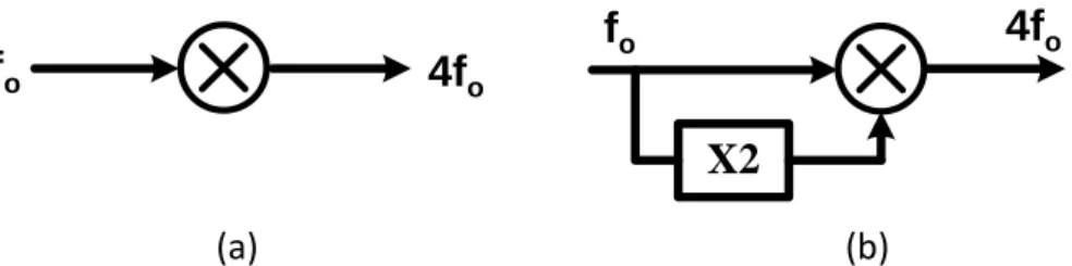
The proposed architecture is shown in figure 3.6. Figure 3.6(a) describes the concept of the circuit in figure 3.5. The fundamental signal f0 through nonlinear
devices to directly generate the signal 4f0. Figure 3.6(b) shows an idea to upgrade the
amount of 4f0, which start with the direct generation and then we add a way of
sub-harmonic mixing. The idea of circuit implementation may be shown in figure 3.7. It clearly reveals that the current sinks now provide not only DC bias current, but also AC injection current at frequency 2f0. In other words, as far as possible no additional
DC power are required to yield this AC injection current. However, the question is how much benefit we gained by this sub-harmonic mixing.
By way of some nonlinear analysis we can explain how it works theoretically. Such as Volterra series, which is a mathematic approach, can help us comprehend the nonlinear behavior in more detail. So the section 3.3 will discuss the solutions of Volterra series to analyze the circuit like as figure 3.7. On the other hand, if you have
f0 (Q-)
f0 (Q+) f0 (I+) f0 (I-)
21
understood the Volterra series more or if you merely intend to know the design methods, you can pass over the next section and move on to the section 3.4 directly. In Section 3.4 we will carry on the design procedure of the proposed quadrupler.
3.3 Nonlinear Analysis of Sub-harmonic Mixing
In this section we study how to analyze the weakly nonlinear behavior of analog integrated circuit. When we use simulation tool to get the response of output harmonics, simulation results can not clearly present information of how the circuit works. As we all know, nonlinear behavior due to the physical structure is complicated. General simulation tools use BSIM4 model to consider and compute the
f0 (Q-) f0 (Q+) f0 (I+) f0 (I-) Ibias+ Iinject (DC) (AC@2f0) Ibias+ Iinject (DC) (AC@2f0)
Figure 3.7 The concept of circuit implementation of the proposed quadripler.
fo 4fo
4fo fo
X2
(a) (b) Figure 3.6 The architecture of proposed quadrupler.
22
behavior of a MOS transistor. By this meticulous model we could get the precise simulation results, but it can not clearly tell us each contribution and how it generates. A mathematic approximately model such as Volterra series can help us get some information in more detail.
Volterra series describe the output response of a nonlinear system as the sum of the harmonics of a first-order operator, a second-order one, a third-order one, and so on. Every operator is describe either in the time domain or in the frequency domain with a kind of transfer function, called Volterra kernel. In principles, the method of Volterra series describing a nonlinear system is as like the way that Taylor series approximate an analytic function. The higher input amplitude, the more terms of series need to be taken into account in order to have precise representation of the system. For very high amplitude, the series diverges, just as Taylor series. The most difference between Taylor series and Volterra series is the ability to deal with a circuit with memory. Volterra series can analyze the memory circuit including the inductors and capacitors which retain phase information, but Taylor series can not. It deals with a memory-less circuit more properly.
For a one-port system, Volterra kernel can be computed to get the output response for any input signal. However, for multiple-port circuit, Volterra kernel become formation of tensors, so the calculation also become more arduous. Now a direct calculation method (DCM), a variant Volterra series approach, directly calculates the required response repeatedly so that it does not make use of tensors. The DCM calculate the nonlinear response at desired frequency directly, and if you want to obtain another response at other frequency, nearly calculate repeatedly. For mixer circuits, such as Gilbert mixer, they are two-port system with two inputs of signal RF and signal LO. Therefore, the DCM is more appropriate for the nonlinear analysis. The nonlinear analysis of the sub-harmonic mixer shown in figure 3.8 (not
23
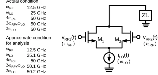
including bias circuit ) is implemented with DCM. As we have mentioned in the last section, this is a half-circuit of the proposed quadrupler. Figure 3.9 shows its equivalent circuit for nonlinear analysis. The circuit is excited by three different input ports, vRF1(t) and vRF2(t) which are differential signals in principle are at frequency
RF, and iLO(t) is at frequency LO, respectively.
1 Re 1 RF j t RF RF v t V e (3.1)
2 Re 2 RF j t RF RF v t V e (3.2)
Re
j LOt
LO LO i t I e (3.3) Under steady-state conditions, every node voltage vx(t) consists of harmonics andintermodulation of signal RF and signal LO as shown in equation (3.4).
vRF1(t)
ZL
vRF2(t)
iLO(t)
Figure 3.8 The sub-harmonic mixer, which is the half circuit of the proposed quadrupler with the differential-pair topology.
Cgb Csb Cdb Cgs Cgd Cdb Cgd Cgs Csb Cgb 2go vRF2(t) vRF1(t) Zs iLO(t) Zd 1 2 3 4 S D G1 G2 B1 B2 Zg Zg Id1 Id2
24 , ( ) , 1 , 1, 2, 3, 4 2 RF LO j m n t x mn m n V e x
(3.4) where vx,mn denotes the voltage at the node x at frequency mRF+nLO. The first thingin this section is to explain the way to compute the complex phasor Vx,mn. We define
the matrix U(t) as the matrix of each node's voltage responses shown in equation (3.5) ,and this is not including parameters concerning negative frequency.
2 1,10 1.01 1,20 1,11 1,02 1 2,10 2.01 2,20 2,11 2,02 2 3,10 3.01 3,20 3,11 3,02 3 4,10 4.01 4,20 4,11 4,02 4 1 1 2 1 2 1 2 2 RF RF LO j t j t j j t e V V V V V v t e V V V V V v t U t e V V V V V v t e V V V V V v t 2 ... 1 2 LO RF LO t j t e
2 10 01 20 11 02 2 1 1 2 1 2 ... 1 2 1 2 2 RF RF LO RF LO LO j t j t j t j t j t e e U U U U U e e e (3.5)The drain current is a function of vds, vds, and vbs so that it can be expanded by a
three-dimensional power series as be shown in equation (2.24), rewrite in equation (3.6) and high orders are omitted.
2 2 2
2, 2, 2, 2, & 2, & 2, &
3 3 3 2 2 3, 3, 3, 3,2 & 3,2 & 3, &2 m mb o m mb m o mb o m mb o m mb m o m mb d m gs mb bs o ds g gs g bs g ds g g gs bs g g gs ds g g bs ds g gs g bs g ds g g gs bs g g gs ds g g gs i g v g v g v K v K v K v K v v K v v K v v K v K v K v K v v K v v K v 2 2 2 2
3, &2 3,2 & 3, &2 3, & & ... m o mb o mb o m mb o bs g g gs ds g g bs ds g g sb ds g g g gs bs ds v K v v K v v K v v K v v v First-order Second-order Third-order (3.6)
2 ,10 ,01 ,20 ( ) 2 ,11 ,20 Re Re Re Re Re ... LO RF RF RF LO LO j t j t j t x x x x j t j t x x v t V e V e V e V e V e 25
The nonlinear coefficients are defined as equation (2.13), (2.19) and (2.21) for one-, two-, and three- dimensional. Wright again in equation (3.7), (3.8), and (3.9)
1 , 1 ! C n n g n v V f v K n v (3.7)
1 2 , & , 1 1 ! ! m m jg m j g j m j f u v K u v j m j (3.8)
1 2 3 , & & ( ) , , 1 1 1 ! ! ! m m jg kg m j k g j k m j k f u v w K u v w j k m j k (3.9) 3.3.1 First-Order ResponseFirst-order response is linear and can be obtained by Kirchoff's laws. Use the technique of superposition to get the individual response for frequency RF and LO.
For instance, as we calculate the response to the inputs vRF1 and vRF2 which are at the
same frequency RF, set iLO to be zero. The AC equivalent circuit is as same as figure
3.2 but iLO taking off. Then make use of Kirchoff's current and voltage laws, we can
get four equations at nodes marked ①, ②, ③, and ④, as follow.
①
3 1 4 1 1 3 2 4 2 2 1 1 2 2 2 2 gd gd db m m mb ZL o sC v v sC v v sC v g v v g v v g v g v g v v (3.10) ②
2 3 2 4 2 2 1 2 2 3 2 4 2 2 2 2 ZS m m mb o sb gs gs g v g v v g v v g v g v v sC v sC v v sC v v (3.11) ③ gZG
vRF1v3
sC vgb 3sCgs
v3v2
sCgd
v3v1
(3.12) ④ gZG
vRF2v4
sC vgb 4sCgs
v4v2
sCgd
v4v1
(3.13) Make a arrangement and transform the equation into a matrix, write down the matrix equation:26
2 2 2 2 0 0 gd db o ZL m mb o gd m gd m o m mb o gs sb ZS m gs m gs gd gs gb gs ZG gd gd gs gb gs ZG gd sC sC g g g g g sC g sC g g g g g sC sC g g sC g sC sC sC sC sC g sC sC sC sC sC g sC 1,10 2,10 3,10 1 4,10 2 0 0 ZG RF ZG RF v v v g v v g v (3.14) where s jRFEquation (3.14) can write in a general form:
RF
10 1,10 Y j U IN (3.15) and 2 2 2 2 0 0 gd db o ZL m mb o gd m gd m o m mb o gs sb ZS m gs m gs gd gs gb gs ZG gd gd gs gb gs ZG gd sC sC g g g g g sC g sC g g g g g sC sC g g sC g sC Y s sC sC sC sC g sC sC sC sC sC g sC 1,10 2,10 10 1,10 3,10 1 4,10 2 0 0 ZG RF ZG RF v v U and IN v g v v g v where Y(s) is a transconductance matrix. U10 is a matrix of the voltage response, and IN1,10 is a vector whose only nonzero components are terms in the network equations
at frequency RF. Then the linear response can be got by the inverse operation. In the
same way, the first-order response to the input signal at other frequencies can be identified by the following equations:
1,01 2,01 1 1 01 1,01 3,01 4,01 0 0 0 LO LO LO v v i U Y j IN Y j v v (3.16)27
1, 10 2, 10 1 1 10 1,01 3, 10 4, 10 0 0 0 LO RF RF v v i U Y j IN Y j v v (3.17) ....Equation (3.17) states the voltage responses at negative frequency, it is for the requirement of the high-order calculation, we will investigate in the following section.
3.3.2 Second-Order Response
The second-order response can be identified by the information from the first-order. As the same linearized network as the precious step solved again to get matching responses, but the input signal sources are different now. Instead of the external excitation, so-called nonlinear current source of order two must be applied. Each nonlinearity in the equivalent circuit generates a nonlinear current source. This second-order nonlinear current source can be obtained by the following method. We simplify our question by considering only one nonlinear current source at one time. Take nonlinearity K2,gm for computing at first, the equivalent circuit for the analysis of
second-order response is shown in figure 3.3, and we write the nodal equation at node 2 and get the following equation.
2 3 2 4 2 2 1 2 2 3 2 4 2 2 2 2 2 S Z m m mb o sb gs gs NL g v g v v g v v g v g v v sC v sC v v sC v v i (3.18)where iNL2 is the second-order nonlinear current source of a nMOS transistor shown in
equation (3.19).
2 2 2
2 2, m 2, mb 2, o 2,m& mb 2, m& 2, mb& o
NL g gs g bs g ds g g gs bs g go gs ds g g bs ds i K v K v K v K v v K v v K v v (3.19) Cgb Csb Cdb Cgs Cgd Cdb Cgd Cgs Csb Cgb 2go Zs Zd 1 2 3 4 S D G1 G2 B1 B2 Zg Zg Id1 INL2,1 INL2,2 Id2