J. Electrochem. Soc., Vol. 144, No. 1, January 1997 The Electrochemical Society, Inc. 311 AppI. Phys., 77, 3710(1995).
10. 5. M. Hu, AppI. Phys. Lett., 36, 561 (1980).
11. J. Furukawa, N. Iwaoka, and H. Furuya, Mater. Sci.
Forum, 196-201, 1725 (1995).
12. W. Wijaranakula and H. D. Chiou, AppI. Phys. Lett.,
64,1030 (1994).
The Influence of Precleaning Process on the Gate Oxide Film
Fabricated by Electron Cyclotron Resonance Plasma Oxidation
Kow-Ming Chang, Chii-Horng Li, Fu-Jier Fahn, Jung-Yu Tsai, Ta-Hsun Yeh, Shih-Wei Wang, and Ji-YiYang Departmentof Electronics Engineering and Institute of Electronics, National Chiao Tang University, Hsin-Chu, Taiwan
ABSTRACT
The influence of the precleaning process on the characteristics of 5i02 film grown by using electron cyclotron reso-nance (ECR) plasma oxidation at room temperature is presented in this work. We find that the growth rate, electrical properties, and reliability of the ECR plasma grown oxide is improved by this precleaning step. Two growth mechanisms are found which determine the electrical properties of the plasma grown oxide. The plasma damage is also discussed. We find that plasma oxidation produces little plasma damage in our experiments. Excellent ECR plasma grown silicon diox-ide with good electrical properties and reliability characteristics are obtained by this precleaning technique.
Infroduction
The formation of low temperature silicon dioxide is needed in some device structures such as thin film transis-tors (TFT5) for displays, SiGe metal oxide semiconductor field effect transistors (MOSFETs) etc. For this require-ment, the plasma enhanced chemical vapor deposition (PECVD) oxide' or liquid phase deposited (LPD) oxide2 are used to meet the low temperature issues. However, the growth rate and electrical properties of these methods are not easily controlled. On the other hand, the fabrication of a thin Si02 dielectric by plasma oxidation has been stud-ied.3-7 It has been shown that the interface between the deposited 5i02 film and Si substrate can be improved by applying plasma oxidation just before film deposition.' The minimum interface states density was as low as 4 X
1010cm2eV'. Besides, the electrical characteristics (e.g.
mobility, D10, etc.) are better than those of chemical vapor deposition (CVD) SiO,4 as they are applied to fabricate the gate oxide of TFT devices. In addition, good electrical properties of gate oxide with plasma N20 annealing has been obtained.3 The purpose of using N20 is to add some nitrogen atoms into 5i02 film which improves the
reliabil-ity of this thin film.09
It is also well known that the surface condition before oxidation determines the quality of the as-grown silicon dioxide. However, in previous studies, there are rarely reports about the influence of plasma precleaning on the quality of SiO2 films grown by plasma oxidation. Plasma N2O has been used to grow an oxynitride film before remote PECVD 5i02;''°" however, the key concept is that growing a plasma oxide yields a better interface between CVD 5i02 and Si. Also, the electrical/reliability properties of the plasma grown SiO3 film are rarely discussed. Therefore, in this work, we study plasma grown SiO2 at room temperature with and without precleaning steps. Their growth rates, interface quality, and electrical relia-bility are discussed.
Experimental
The ECR plasma system used in our experiment is shown in Fig. 1. The coils surrounding the plasma cham-ber will generate an 875 gauss magnetic field density in the plasma chamber and 2.45 GHz microwaves are fed from the top of the plasma chamber. The substrate holder is approximately 18 cm below the plasma extraction port and is maintained at room temperature in our experi-ments. The substrate holder is not biased. The gas is injected into the plasma chamber and will be excited to become plasma by the magnetic field and the microwaves.
p-Type (100) 15 to 25 11 cm Si wafers are used as the
oxi-dation substrate. The process pressure is fixed at 1 mTorr. After initial cleaning, a wafer is transferred into the reac-tion chamber. The base pressure of our ECR system is about 1 X 10⁻⁶ Torr.The oxide thickness is measured by ellipsometer with fixed refractive index 1.462. For the study of electrical properties and the effective oxide thick-ness determination, poly silicon MOS capacitors are fabri-cated on the same silicon wafer. After plasma oxidation, 300 nm poly-Si is deposited at 620°C by a low pressure chemical vapor deposition (LPCVD) system and then fol-lowed by 850°C POC13 doped for 30 mm. A 500 nm thick aluminum film is then deposited and patterned. The sam-ple back side is also deposited with a 500 nm aluminum film as contact. Postmetallization annealing (PMA) is done at 400°C for 30 mm in N2 ambient. The capacitor areas are
3 X
10
and 6.28 X10'
cm2 with circular shapes.Except for those specifically mentioned, the flow rates of the gases used in our experiments are fixed at 50 sccm and the precleaning time is fixed at 10 mm. The micro-wave power is 220 W for the precleaning step and 250 W for the plasma oxidation. During electrical measurement,
02, P42, NH3 gas injection
Fig. 1. Schematic diagram of the ECR plasma system.
I 2.45 0Hz
micro-wave
N
N
N Magnetic coil
) unless CC License in place (see abstract).
ecsdl.org/site/terms_use
address. Redistribution subject to ECS terms of use (see
140.113.38.11
312 J. Electrochem. Soc., Vol. 144, No. 1, January 1997 The Electrochemical Society, Inc.
the capacitors are tested at accumulation (negative gate biased). The interface states are determined by quasi-sta-tic and high frequency (1 MHz) current-voltage (C-V) measurement. For the measurement of cumulative distrib-ution of the oxide reliability, 50 MOS capacitors are
meas-ured for each sample.
Resultsand Discussion
Theinfluence of precleaning on oxide thickness—Figure
2 shows the silicon dioxide thickness with different plasma precleaning conditions. After precleaning, plasma oxida-tion is performed to grow silicon dioxide. The thickness is determined by an ellipsometer with a fixed refractive index of 1.462. It is easily seen that the thickness is greater for the Si02 with the precleaning process than that with-out the precleaning step. When NH3 gas is used to perform
the precleaning process, the highest growth rate is
obtained.
In order to investigate the precleaning effect, all of the samples have the same growth conditions except that some will undergo the precleaning step and others are not exposed to this process. Apparently, different oxide thick-nesses are obtained. This means that the initial surface condition before plasma oxidation determines the growth kinetics. We think that although a standard RCA initial cleaning is performed before the sample is transferred into the ECH system, the native oxide on the silicon surface still existed. After the 02 plasma is initiated, the initial oxygen plasma will "see" the surface of native Si02 (not the bare Si atoms in the substrate). The oxygen species dif-fuse through this native oxide film and then oxidize the silicon atoms. Thus, the oxidation is retarded, which low-ers the oxidation rate. On the other hand, with the pre-cleaning process in the vacuum chamber before plasma oxidation, the native oxide is removed and the silicon sur-face dangling bonds are activated. This leads to the high-er growth mechanism because of direct reactions with this cleaned/activated silicon surface atoms and thus the high-er growth rate. In othhigh-er words, the oxidation reaction is continuous and the initial surface condition determines the growth mechanism. If the initial growth condition is determined, then the oxidation mechanism is decided. These two different growth mechanisms will affect the electrical properties of the plasma grown oxide.
Electrical properties —The breakdown characteristics of the ECR plasma grown oxide mentioned above are determined by two methods: the time-zero dielectric breakdown experiment and constant current stress under Fowler-Nordheim (F-N) tunneling. The effective oxide thickness was measured by the C-V method. The
break-down field (BF) distributions of different samples are
shown in Fig. 3. The capacitor area is 3 x 10 cm2.
Because the growth rate is too low for the oxygen only plasma used without pretreatment, we added some N2 gas into 02 plasma to improve the growth rate. The gas ratio is
N2/02 =9(sccm)/50 (sccm) and the growth pressure is also
at 1 mTorr. This sample (WO) is used for the case without precleaning for electrical measurement, and its BF distri-bution is shown in Fig. 3. The oxide thickness of WO is 7 nm. In Fig. 3, the curve of WP-N2 is the Si02 with 7 nm thickness precleaned by N3 plasma and the curve of WP-NH3 is the 5i02 with 7.2 nm thickness precleaned by WP-NH3 plasma.
The BF distributions of ECR oxide with and without pretreatment (WO, WP-N2, and WP-NH3) are all tightly distributed in the higher breakdown field (—12 —13
MV/cm) region and very small B-mode breakdown12
distri-butions exist. Note that the dielectric breakdown fields are categorized into three modes: A, B, andC modes. The A mode can be attributed to the pinhole of the gate oxide which causes nearly zero breakdown field (< 1 MV/cm). The B mode is caused by a weak spot of oxide with inter-mediate breakdown field (1 MV/cm — 8 MV/cm). The C mode is due to the defect-free oxide breakdown (intrinsic dielectric breakdown). The results in Fig. 3 reveal that there is a small number of defects (such as pinholes, weak spots, etc.) in our samples, which result in lower dielectric breakdown field. From this figure, the lower value break-down field distribution of samples of WP-N2 and WO are smaller than that of WP-NH3. This means that with the N3 plasma precleaning step, the BF characteristics of 5i02 were not influenced; however if the NH3 plasma preclean-ing is used the BF characteristics are slightly degraded.
However, for the charge-to-breakdown (Qbd) distributions,
the samples with the precleaning steps are better than those without the precleaning processes. This can be seen
in Fig. 4. The Qbd wasmeasured by applying a constant —200 mA/cm2 F-N tunneling current density on the MOS capacitor with an area of 6.28 X
l0
cm2. It can be seen that the Qbdofall the ECR plasma oxidized oxide can be achieved —9 C/cm2 under the —200 mA/cm2 stressing.From this figure, we found that samples of WO exhibit
sig-nificant distributions for cumulative failure less than 60%. However, samples of WP-N2 and WP-NH3 do not exhibit the phenomenon of WO. From the results of Fig. 3 and 4, we conclude that with the N2 plasma precleaning step, the breakdown field and reliability characteristics of
gate oxide grown by ECR plasma oxidation can be
improved.
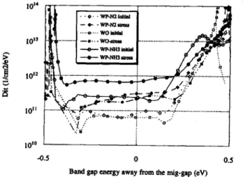
The interface states of samples WO, N2, and WP-NH3 are shown in Fig. 5. The initial midbandgap interface
It
I
CI
I
80 70 60 50 40 30 20 10 0 100 80 60 40 20 0 10 20 30 40 50Growthtime (minute)
0
Fig. 2. The oxide thickness with different growth lime. The curve of p02 is the sample without precleaning, the curve of NH3-02 uses NH3 plasma precleaning for 10 mm, and the curve of N2-02 uses N2
plasma precleaning for 10 mm.
0 2 4 6 8 10 12 14
Effectivebreakdown field (MV/cm)
Fig. 3. The cumulative failure distribution of effective breakdown Field. WO denotes without precleaning, WP-N2 is with N2 preclean-ing, and WP-NH3 denotes NH3 precleaning.
) unless CC License in place (see abstract).
ecsdl.org/site/terms_use
address. Redistribution subject to ECS terms of use (see
140.113.38.11
J. Electrochem. Soc., Vol. 144, No. 1, January 1997 The Electrochemical Society, Inc. 313 0 2 4 6 Charge-to-breakdown (Ckm2) 100 0 8 tO
Fig. 4. The cumulative failuredistributionof Q,,,.
statesare 6.5 X 10¹⁰, 8 X lOll, and 2.4 X 1011 cm2
eV' for
WO, WP-N2, and WP-NH3, respectively. It can be seen that
the initial D1 of WO is lower than those of the other two, and sample WP-NH3 has the highest D,. If the nitrogen is in the Si02, the reliability characteristics (such as Ag,,
AVT, AD18, Qbd,etc.)are improved.0 Furthermore, if nitrida-tion is performed with NH3 gas, higher interface states
generation may be formed.'3'14 The precleaning gases used
in our experiments contain the nitrogen "N" species; this pretreatment step will have some nitridation effect, and the D1 of those with the precleaning step will be slightly
higher. The worst case is found inthe NH3 precleaned sam-ple (WP-NH3). However, the Qbddistributions are better for samples with the "N" related precleaning step due to the "N" incorporation during the precleaning which can
be seen from the results of Fig. 4. Although the sample WO
(grown by mixed N2/02 plasma) may incorporate some nitrogen atoms into oxide, the improvement of Qbdis smaller than for the other two samples.
In order to study the interface quality of the plasma grown oxide, changes of the midgap interface states (AD,,)
after constant —10 mA/cm2 current density stressing for 10 s for samples of WO, WP-N2, and WP-NH3 are investigat-ed. The AD,8 of WO, WP-N,, and WP-NH3 are about 2.3 X 10", 2.3 )< 1011, 4 x 10k' cm2 eV'. It can be found that AD1 of WP-N2andWO are about the same, but AD,8 of WP-NH3
was found to be higher than the other two samples. This may be attributed to a weaker NH3 precleaning/mtrida-tion effect, and more precleaning/nitridaprecleaning/mtrida-tion should be
used.13"4 Although using N3 precleaning will result in bet-ter Qbdperformance,the resistance of AD11 was not
signif-icantly improved.
The gate voltage shift during —200 mA/cm2 constant current density stress is investigated in Fig. 6. It is inter-esting to note that no negative charge trapping phenome-non exists in the oxide of WO and WP-N2. However, the oxide of WP-NH3 shows the trend of negative charge trap-ping. This may be attributed to some hydrogen atoms in the NH3 gas which incorporate into Si02 and these H atoms are the sources of electron trapping which cause negative gate voltage shift.'5'16 Thus, a slightly negative charge trapping effect is seen in WP-NH3. It should be noted that positive charge trapping dominated for all of the samples. This phenomenon is different from the results of our previous study,'7 in which the negative charge trap-ping dominated, and no positive charge traptrap-ping was observed. The different trapping effect existing in silicon dioxide grown by the same method was still observed in
another study18 even in the thermal grown oxide. This
phe-nomenon is still not clear presently.
The effect of plasma damage.—An important considera-tion of using plasma oxidaconsidera-tion is that the film growth in the plasma ambient will be damaged by the plasma. In order to identify this damage, we transferred an oxide grown by dry 02 at 900°C in a conventional furnace with 5.6 nm thickness into our ECR system, then we excited the 02 plasma to grow oxide. The final effective oxide thick-ness is 7 nm. The poly-Si gate MOS capacitor was fabri-cated for electrical measurement, while the processes of MOS capacitor fabrication are the same as described in the Experimental section. Ramped I-V curves of this dam-aged oxide (DO) are shown in Fig. 7. It is clearly seen that the plasma-induced leakage current is higher due to the plasma damage. However, our ECR plasma grown Si03 (WP-N3) does not have this higher plasma-induced
leak-age. Even in the sample of WP-NH3, which has a higher
pre-tunneling leakage current due to the NH3 precleaning step,
it does not have this larger plasma-induced leakage current. This indicates that very low plasma damage was done in our ECR plasma oxidized Si02 film with precleaning step.
Above, we find that there are two different growth mechanisms, that is, the oxidation with "initial" oxide
existing on the Si surface and the oxidation with
cleaned/activated Si surface. Besides, these different growth mechanisms will determine the quality of oxide. Before growing sample DO, a 5.6 nm Si02 has been on the Si surface and the growth mechanism is different from that of sample WP-N2 with a cleaned surface. The possible explanation may be that the worst plasma damage will build in the initial stage of plasma oxidation but not in the plasma turn-off stage. Thus, the sample with "initial"
0.05 0.04 0.03
I
0.02 0.01 0Fig. 6. The gate voltage shifts during constant —200 mA/cm2 cur-rent density stressing.
i0°
10°
10"
1010
-0.5 0 0.5
Bandgap energy awayfrom themig-gap (eV)
Fig. 5. The interface states evaluation of the samples of WO, WP-N2, and WP-NH3.Thesolid symbols mean the D8 after constant —10 mA/cm2 current density stressing for 10 s.
0 I 2 3 4 5
Suess time (
) unless CC License in place (see abstract).
ecsdl.org/site/terms_use
address. Redistribution subject to ECS terms of use (see
140.113.38.11
314 ,.L Electrochem. Soc., Vol. 144, No.1, January 1997 Electrochemical Society, Inc.
I
Gate voltage (WV)
Fig. 7. The I-V curves of Si02 with different plasma treatment
con-ditions. The curve of DO represents the growth with an initial 5.6 nm thermal oxide to obout 7 nm by plasma 02 oxidation. insulatorof silicon dioxide will build negative charges on the insulator surface to maintain the plasma condition which in turn will cause damage. However the sample of WO with native oxide before plasma oxidation does not have this plasma-induced leakage current. This is due to the fact that native oxide is very thin (about 0.3 nm) and hence the plasma damage is very small. For thicker "ini-tial" oxide on Si surface, the charges which are built up in the initial oxidation stage are larger in the thicker Si02 film, and hence higher plasma damage induced leakage current will be seen. However, for the cleaned surface, negative charges are built up in the Si (not in the insula-tor), and lower or even no plasma damage is expected. It should be mentioned that if the plasma oxidation pressure is reduced, the oxide will be damaged by the higher ener-getic ion bombardment even with the precleaning step. However, the plasma-induced leakage current is still not significant (not shown here).
Conclusion
Excellentgate oxides grown by ECR plasma oxidation
have been obtained. The Eba is about —13 MV/cm and the Qba can reach —9 C/cm2 under —200 mA/cm2 constant
cur-rent density stressing. In addition, the quality of the plas-ma grown Si02 can be improved with N2 plasplas-ma preclean-ing step. There are different growth mechanisms for the
samples with and without the precleaning processes. Without the precleaning step, plasma damage is higher. Besides, the plasma damage may build at the initial stage of the plasma oxidation.
Acknowledgments
Support of this work by the ROC National Science Council, Engineering Division under Grant NSC 85-2215-E009-061 is gratefully acknowledged. The authors are indebted to the Reviewers for a careful reading and criti-cism of the manuscript.
Manuscript submitted Jan. 5, 1996; revised manuscript
received Oct. 15, 1996.
National Chiao Tung University assisted in meeting the publication costs.
REFERENCES
1. T Fuydi, T. Oka, and H. Matsunami, Jpn. J. AppI.
Phys., 33, 440 (1994).
2. C. F. Yeh, S. S. Lin, C. L. Chen, and Y. C. Yang, IEEE
Electron Device Lett., EDL-14, 403 (1993).
3. P C. Chen, Klaus, Y. J. Hsu, H. L. Hwang, and J. Y. Lin, J. Appl. Phys., 76, 5508 (1994).
4. P W Li, E. S. Yang, Y. F. Yang, J. 0. Chu, and B. S. Meyerson, IEEE Electron Device Lett., EDL-15, 402
(1994).
5. J. Y. Lee, C. H. Han, and C. K. Kim, ibid., EDL-15, 301 (1994).
6. D. W. Hess, Mater. Res. Soc. Symp. Proc., 236, 191
(1992).
7. D. A. Carl, D. W. Hess, M. A. Lieberman, 1'. D. Nguyen, and R. Gronsky, J. Appl. Phys., 70, 3301 (1991).
8. H. Hwang, W. Ting, D. L. Kwong, and J. Lee, IEDM,
421 (1990).
9. C. G. Sodini and K. S. Krish, ibid., 617 (1992). 10. T Yasuda, Y. Ma, S. HaBermehl, and G. Lucovsky,
Appl. Phys. Lett., 60, (1992).
11. D. R. Lee, C. G. Parker; J. Hauser, and G. Lucovsky, J.
Vac. Sci. Technol, B13, 1788 (1995).
12. K. Yamabe and K. Taniguchi, IEEE Trans. Electron
Device, 32, 423 (1985).
13. W. Yang, R. Jayaraman, and C. G. Sodini, ibid., ED-35, 935 (1988).
14. T. Hori, H. Iwasake, and K. Tsuji, ibid., ED-35, 904
(1988).
15. H. S. Momose, T. Morimoto, Y. Ozawa, M. Tsuchiaki, M. Ono, K. Yamabe, and H. Iwal, IEDM Tech. Dig.,
359 (1991).
16. T. Hori, H. Iwasaki, Y. Naito, and H. Esaki, IEEE Tran. Electron Device, ED-34, 2238 (1987).
17. K. M. Chang, C. H. Li, F J. Fahn, J. Y. Tsai, T. S. Yeh,
and W. S. Wang, To be published.
18. H. Fukuda, 11 Arakawa, and S. Ohno, Jpn. J. Appl.
Phys., 29, L2333 (1990).
0 1 2 3 4 5 6 7 8
) unless CC License in place (see abstract).
ecsdl.org/site/terms_use
address. Redistribution subject to ECS terms of use (see
140.113.38.11