The electrical characteristics and reliability of the
F-ions-im-planted poly-Si TFTs were reported for solid phase crystallization
(SPC) and excimer laser crystallization (ELC) methods
respec-tively. The thermal annealing causes F-ions to pile up at the
poly-Si interface, without the initial pad oxide deposition. With
the introduction of fluorine in poly-Si film, the trap state density
was effectively reduced. Also, the presence of strong Si-F bonds
enhances electrical endurance against hot carrier impact by using
F-ions-implantation. These improvements in electrical
character-istics are even obvious for the ELC poly-Si TFTs compared to the
SPC ones.
Index Terms—Excimer laser crystallization (ELC), F-ions
im-plant, polycrystalline silicon thin-film transistors (poly-Si TFTs),
SPC.
I. I
NTRODUCTIONI
N RECENT YEARS, the polycrystalline silicon thin-film
transistors (poly-Si TFTs) were widely used in many
application, especially for active-matrix liquid phase crystal
displays (AMLCDs) [1], [2]. The major attraction of the poly-Si
TFTs in AMLCDs lies in the significantly improved carrier
mobility, as well as the ability to integrate the pixel switching
elements, panel array, and peripheral driving circuit on the
same substrate [3]–[5]. Low temperature technology is required
to realize commercial flat plane display (FPD) on inexpensive
glass substrate when fabricating high performance poly-Si
TFTs, since the maximum process temperature is limited to
Manuscript received March 15, 2006; revised May 20, 2006; June 28, 2006; and August 17, 2006. This work was performed at National Nano Device Lab-oratory. This work was supported by the National Science Council of the Re-public of China under Contracts NSC 009-283, NSC 95-2221-E-009-270, NSC 95-2120-M-110-003, and NSC 95-2221-E-009-254-MY2, and supported in part by MOEA Technology Development for Academia Project 94-EC-17-A-07-S1-046.
C.-H. Tu, C.-Y. Yang, L.-W. Feng, C.-C. Tsai, L.-T. Chang, S. M. Sze, and C.-Y. Chang are with the Institute of Electronics, National Chiao Tung Univer-sity, Hsin-chu 300, Taiwan, R.O.C.
Y.-C. Wu is with the Department of Engineering and System Science, Na-tional Tsing-Hua University, Hsinchu, Taiwan, R.O.C.
T.-C. Chang is with the Department of Physics and Institute of Electro-Op-tical Engineering, National Sun Yat-Sen University, Kaohsiang 804, Taiwan, R.O.C., and also with National Nano Device Laboratories, Hsin-Chu 300, Taiwan, R.O.C. (e-mail: [email protected]).
P.-T. Liu is with the Department of Photonics and Display Institute, National Chiao Tung University, Hsin-Chu 300, Taiwan, R.O.C. (e-mail: ptliu@mail. nctu.edu.tw).
Color versions of one or more of the figures are available online at http:// ieeexplore.ieee.org.
Digital Object Identifier 10.1109/JDT.2006.890707
to recrystallize amorphous silicon (a-Si) to poly-Si at low
tem-perature fabrication process. The SPC process, requiring 24–48
h, is a time consuming procedure, which obviously affects the
throughput and thermal budget of fabrication processes [6].
Furthermore, the resultant lower field effect mobility will limit
the development for SPC poly-Si TFTs for small grain size.
The excimer laser system can create larger grain size and little
intra-grain defect than using conventional SPC method [7], [8].
Furthermore, the laser annealing process is not a high
tempera-ture fabrication and a rapid process. Hence, the laser annealing
system is generally applied in flat plant display application.
However, the difference of thermal expansion coefficient for
molten poly-Si and buffer oxide causes serious mechanical
stress during the ELC thermal annealing process.
The off-state electrical characteristics of poly-Si TFTs are
dominated by the trap state density of grain boundary. Based on
this issue of poly-Si TFTs, the method for reducing trap state
density is applied to enhance the electrical characteristics. The
typically used passivation methods are hydrogen plasma
ment and ion implantation [9]–[11]. The hydrogen plasma
treat-ment is widely used to passivate trap states at poly-Si grain
boundaries to avoid the undesirable leakage current [9].
How-ever, it is difficult to control hydrogen concentration precisely
in the poly-Si TFTs [9]. Also, the Si-H bonds are not strong
enough against the hot carrier impact, during high electrical bias
operation. One of the promising strategies on the electrical
provement of the poly-Si TFTs was proposed using F-ion
im-plantation to eliminate the defects in the grain boundaries [10],
[11]. Several proposed F-implantation technologies are
summa-rized as followed. In the initial study, the pad oxide deposition
on a-Si layer before crystallization was implemented to cause
F-ions to pile up at the interfaces between the poly-Si and the
oxide to eliminate the strain bonds. Also, F-implanted poly-Si
TFTs without pad oxide deposition step were proposed to study
in our previous work [12], [13]. The oxidized a-Si film on
sur-face during thermal crystallization provides the driving force for
the implanted fluorine elements to segregate on the surfaces.
The proposed modified F-implantation passivation technology
reduces manufacture process steps, and exhibits high potential
for the application on AMLCDs. The undesirable strain bonds
in the interface between poly-Si and SiO are passivated by
using F-ions-implantation. Furthermore, the segregated F-ions
at the interface between poly-Si and buffer oxide eliminated the
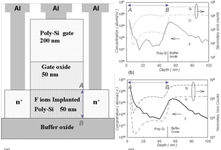
Fig. 1 (a) Cross-section of F-ions incorporated poly-Si TFTs. (b) The SIMS analysis of F-ions in poly-Si channel after SPC. (c) The SIMS analysis of F-ions in poly-Si channel after ELC.
strain bonds which are generated during rapid excimer laser
an-nealing, leading to the superior electrical characteristics [14]. In
addition, the strong Si-F bond replaced the weak Si-H and Si-Si
bonds, resulting in the superior electrical DC stress reliability
compared to standard poly-Si TFTs.
This work investigated the electrical characteristics of
F-im-planted poly-Si TFTs without the initial deposition of pad oxide
before crystallization process. The poly-Si crystallization were
realized by using conventional solid phase crystallization (SPC)
and excimer laser crystallization (ELC). The behavior of
F-im-planted a-Si during the both the above crystallization steps were
discussed. Also, the electrical reliability of poly-Si TFTs using
both the crystallization methods were compared in this work.
II. E
XPERIMENTSThe 50-nm-thick undoped a-Si layer was deposited by
de-composition of pure silane SiH
on oxide-coated silicon wafer
with using low pressure chemical vapor deposition (LPCVD)
system at 550 C. Then the F-ions were implanted to the a-Si
layer without any pad oxide deposited first. The ion implantation
conditions were set at an ion accelerating energy of 11 keV and
the doping dosages are 5
10
cm
. The crystallization for
F-ions-implanted a-Si and standard a-Si was realized by heating
in a furnace at 600 C for 24 h in N ambient and excimer
laser annealing system, respectively. The ELC was realized by
a KrF excimer laser system at room temperature in vacuum
10
torr with a laser energy of 300 mJ/cm . After
pat-terning and etching the active region, the 50-nm-thick
tetraethy-lorthosilicate (TEOS) layer and the 200-nm-thick poly-Si gate
were deposited by LPCVD system. The deposition temperature
of TEOS layer and poly-Si layer are 700 C and 575 C,
respec-tively. The ions are used for the source–drain ion implantation
after patterning and etching the poly-gate. The ion accelerating
energy is 17 keV and the dosage is 5 10
cm
. The activation
was realized by depositing of the TEOS passivation layer using
LPCVD system at 700 C for 3 h. The contact hole regions were
patterned and etched by a buffer oxide etching (BOE) solution.
Finally, the aluminum metallization was performed, followed by
350 C sintering in the thermal furnace for 30 min. The device
cross section is shown in Fig. 1(a).
III. R
ESULTS ANDD
ISCUSSIONThe behavior of F-ions in poly-Si after thermal annealing
was investigated in this work. Fig. 1(b) and (1c) show the
secondary ions mass spectroscope (SIMS) analysis of F-ions
after SPC and ELC, respectively. It is found that the F-ions are
piled up at the surface of poly-Si and the interface between
poly-Si and buffer oxide. Without pad oxide deposited on a-Si
layer, the F-ions are segregated to the poly-Si surface during
recrystallization. Hence, it needs no extra thermal annealing
step and no additional process steps for the F piling up. In
addi-tion, the electrical characteristics of F-ions-implanted poly-Si
TFTs are investigated in this study. Fig. 2 shows the transfer
dosage of 52 10 cm and standard. TABLE I
THEPARAMETERS OF THEPOLY-Si TFTS FORF-IONS-IMPLANTED AND
STANDARDUSINGSPC METHOD ANDELA METHOD
characteristics of poly-Si TFTs for F-ions-implantation dosages
of 5
10
cm
and standard poly-Si TFTs. It is clearly
found that the electrical characteristics are improved with
F-ions-incorporated poly-Si TFTs no matter using SPC method
or ELC method. The major parameters including field-effect
mobility
, threshold voltage
, subthreshold swing
, and trap state density
are summarized in the
Table I. It is considered that the reduction of trap state density
improves the electrical characteristics for the two types of
devices. The fluorine effectively passivates the dangling bond,
leading to lower trap state density. The threshold voltage
is defined as the gate voltage that yields the drain current
nA
. The threshold voltage is greatly
reduced by using F-ions-implantation. The poly-Si TFTs with
reduced
have even more potential for the application on
AMLCD. In addition, the
is greatly improved in this work.
It is found that the
value for poly-Si using SPC method
varies from 19.74 cm
V s to 54.48 cm
V s. Furthermore,
the
value of F-ions-implanted poly-Si TFT (ELC method)
is approximately two times to those of standard (56.65 cm
V s
to 103.94 cm
V s).
Fluorine piled up at the poly-Si/buffer-oxide interface,
con-firmed by SIMS analysis, and passivated the stress-induced
strained bonds to form stronger Si-F bonds due to the high
electronegativity of F atoms. The reduction of trap states
be-tween poly-Si and buffer oxide improves the performance of
the poly-Si TFTs, such as
,
, and
[14]. Hence, the
superior electrical characteristics are attributed to the relaxation
of mechanical stress and trap state elimination in poly-Si TFTs,
especially for using ELC method.
from on-state current is reduced, while
extracted from the
off-state current is increased, indicating that F-ion implantation
effectively reduces the trap state density. The
of off-state
current is increased and the
of on-state current is reduced
for the F-ions-implanted poly-Si TFT, indicating that F
implan-tation alters the trap state density. This result is consistent with
the above discussion. Furthermore, by calculating the trap states
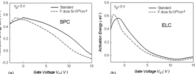
density distribution in the bandgap [16], the trap state
densi-ties for SPC method and ELC method, are clear reduced with
F-ions incorporation are shown in Fig. 4(a) and (b), respectively.
It is consistent with the result of activation energy as shown in
Fig. 3(a) and (b). It is believed that the reduced trap states
den-sity causes the enhanced electrical characteristics.
F-ions-incor-porated poly-Si TFTs obtain reduced both the tail states and the
deep states. The reduced deep states lead to decreased
in
n-ch poly-Si TFTs [10]. The tail state reduction improves the
electrical characteristics such as s.s and
value [10], also
compatible with our experimental results.
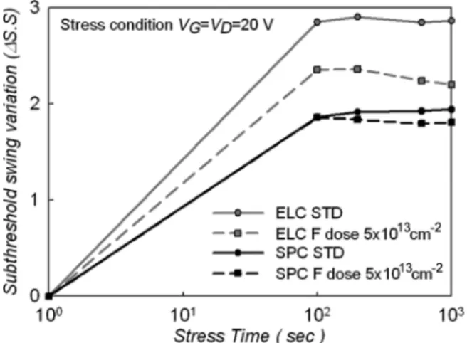
The study also considered the DC stress reliability for
F-ions-implanted poly-Si TFTs. To investigate the device reliability, the
poly-Si TFTs were bias stressed at
and
V
for time duration of 100, 200, 600, and 1000 s. Fig. 5 shows the
values by the SPC method and ELC method.
F-ions-im-planted poly-Si TFTs are found to yield more moderate
values than in standard poly-Si TFTs. Furthermore, hot carrier
multiplication near the drain side degraded the
,
and
values. The
and
also reflect the reliability of the
proposed TFT device. Figs. 6 and 7 illustrate the
and
after DC bias stress and demonstrate the F-ions
implan-tation significantly reduce hot-carrier-induced degradation,
re-spectively. Degradation induced by hot carrier stress can be
at-tributed to the generation of gate oxide/poly-Si interface states
and/or the Si-Si and/or Si-H weak bonds in the poly-Si channel
[17], [18]. The Si dangling bonds are terminated by F-ions, and
the resulting strong Si-F bonding enhances the endurance to hot
carrier impact, thus improving the overall electrical reliability.
The electrical characteristics of poly-Si TFTs using ELC
method are superior to using SPC method for larger grain size
and less intra grain defect. However, the hot carrier impact
is found to degrade the electrical characteristics. Compared
with both crystallization methods, the ELC method indeed
clearly improves the electrical characteristics, such as the
.
The resultant higher
causes more serious degradation on
electrical properties. In contrast, with F-ion implantation the
improvement of DC bias stress reliability for ELC poly-Si TFTs
Fig. 3. (a) The activation energy(E ) of the poly-Si TFTs (SPC) for F-ions-implantation dosage of 5 210 cm and standard atV = 5 V. (b) The activation energy(E ) of the poly-Si TFTs (ELC) for F-ions-implantation dosage of 5 2 10 cm and standard atV = 5 V.
Fig. 4. (a) The trap state distribution in the bandgap of the poly-Si TFTs (SPC) for F-ions-implantation dosage of 52 10 cm . (b) The trap state distribution in the bandgap of the poly-Si TFTs (ELC) for F-ions-implantation dosage of 52 10 cm .
Fig. 5. The threshold voltage variation verse stress time for standard poly-Si TFTs and F-ions-implanted poly-Si TFTs for dosage of 52 10 cm .
is distinct. The lower trap state density for F-ions-implanted
poly-Si TFTs (ELC), as shown in Table I, dominates the
elec-trical improvement. The passivated Si dangling bonds (Si-F) can
resist the hot carrier impact, although higher hot carrier energy
can be obtained from ELC poly-Si TFTs with superior
.
The ELC method clearly improved the electrical
characteris-tics, but degraded the DC stress reliability due to the high carrier
Fig. 6. The on current variation verse stress time for standard poly-Si TFTs and F-ions-implanted poly-Si TFTs for dosage of 52 10 cm .
field effect mobility. However, the F-ions-implantation for ELC
method is more useful to improve the ability to resist the
elec-trical DC stress.
IV. C
ONCLUSIONThe electrical characteristics of the F-ions-implanted poly-Si
TFTs have been investigated in this study. The fluorine ions
seg-regated 5
10
cm
at the poly-Si interfaces by SPC and
Fig. 7. The subthreshold swing variation verse stress time for standard poly-Si TFTs and F-ions-implanted poly-Si TFTs for dosage of 52 10 cm .
ELC processes, which effectively reduces the trap state density
to enhance the electrical characteristics. The improvement of
threshold voltage for SPC and ELC with the incorporation of
fluorine ions are from 6.24 V to 4.78 V and 3.07 V to 1.19 V,
respectively. Also, the strong Si-F bonds instead of the Si-H and
Si-Si bonds can prevent hot carrier impact near the drain side,
and possess superior electrical reliability over typical poly-Si
TFTs. These improvements in electrical characteristics indicate
the proposed F-ions-implantation method is suitable for high
performance poly-Si TFT application in the display fields.
R
EFERENCES[1] H. Oshima and S. Morozumi, “Future trends for TFT integrated circuits on glass substrates,” in IEDM Tech. Dig., 1989, pp. 157–160. [2] S. D. Brotherton, Semicond, “Polycrystalline silicon thin film
transis-tors,” Semicond. Science Tech, vol. 10, pp. 721–738, 1995.
[3] K. Nakazawa, “Recrystallization of amorphous silicon films deposited by low-pressure chemical vapor deposition from Si2H6 gas,” J. Appl.
Phys., vol. 69, pp. 1703–1706, 1991.
[4] T. J. King and K. C. Saraswat, “Low-temperature( 550 C) fabrica-tion of poly-Si thin-film transistors,” IEEE Electron Device Lett., vol. 13, pp. 309–311, 1992.
[5] H. Kuriyama, S. Kiyama, S. Noguchi, T. Kuahara, S. Ishida, T. Nohda, K. Sano, H. Iwata, S. Tsuda, and S. Nakano, “High mobility poly-Si TFT by a new excimer laser annealing method for large area elec-tronics,” in IEDM Tech. Dig, 1991, vol. 91, pp. 563–566.
[6] R. E. I. Schropp, B. Stannowski, and J. K. Rath, “New challenges in thin film transistor (TFT) research,” Journal of Non-Crystalline Solids, vol. 299–302, pp. 1304–1310, 2002.
[7] G. K. Giust and T. W. Sigmon, “High-performance thin-film transistors fabricated using exciter laser processing and grain engineering,” IEEE
Trans. Electron Devices, vol. 45, pp. 925–932, Apr. 1998.
[8] J. S. Im, R. S. Sposili, and M. A. Crowder, “Single-crystal Si films for thin-film transistor devices,” Appl. Phys. Lett., vol. 70, no. 25, pp. 3434–3436, 1997.
[9] I. W. Wu, A. G. Lewis, T. Y. Huang, and A. Chiang, “Passivation ki-netics of two types of defects in polysilicon TFT by plasma hydrogena-tion,” IEEE Electron Device Letter, vol. 12, pp. 181–183, 1993. [10] H. N. Chern, C. L. Lee, and T. F. Lei, “The effects of fluorine
passi-vation on polysilicon thin-film transistors,” IEEE Trans. Electron
De-vices, vol. 41, pp. 698–702, 1994.
[11] J. W. Park, B. T. Ahn, and K. Lee, “Effects of F+ implantation on the characteristics of poly-Si films and low-temperature n-ch poly-Si thin-film transistors,” Jan. J. Appl. Phy., vol. 34, pp. 1436–1441, 1995. [12] C. H. Tu, T. C. Chang, P. T. Liu, H. W. Zan, Y. H. Tai, C. Y. Yang, Y. C. Wu, H. C. Liu, W. R. Chen, and C. Y. Chang, “Enhanced perfor-mance of poly-Si thin film transistors using fluorine ions implantation,”
Electrochemical and Solid-State Letters, vol. 8, pp. G246–G248, 2005.
tion effects in polysilicon thin-film transistors,” IEEE Trans. Electron
Devices, vol. 40, pp. 890–897, 1993.
Chun-Hao Tu received the B.S degree in Physics
from National Sun Yat-Sen University, Taiwan, R.O.C., in 2000. He is currently pursuing the Ph.D. degree at the National Chiao-Tung University, Taiwan, R.O.C. His Ph.D. research interests include fabrication, and characterization of amorphous silicon TFTs, LTPS TFTs and nonvolatile memory.
Ting-Chang Chang is a chair professor in
Deport-ment of Physics, National Sun Yat-Sen University. In his specialty, he has made pioneering contributions to semiconductor device technology, ULSI memory devices and TFT-LCD Displays. He has published 150 articles in SCI journals and obtains 28 patents of United States and 70 patents of Taiwan. Besides, He proposed the project of Industry-Academy Coopera-tion with United Micoelectronics CorporaCoopera-tion to re-search nano-porous low-k materials for ULSI appli-cation, and received great progress and achievement. He thereby had the honor to win the “Award of Industry-Academy Cooperation” from Ministry of Education in 2002. This is a remarkable honor in academic achievement. Recently, he is interested in the study of nonvolatile memory de-vices and nano-dot technology. He and his co-works exhibit greatly performance in these fields.
Po-Tsun Liu received his Ph.D. degree in the
In-stitute of Electronics from the National Chiao Tung University in January 2000. He joined the National Nano Device Laboratory (NDL), Taiwan, as an associate researcher from January 2000, and became the leader of Department of Electro-optics and Bio-technology in March 2004. He has made a great deal of pioneering contributions to low-permittivity (low-k) dielectrics, copper interconnects and thin film transistors (TFTs) technologies. In his research on low-k dielectrics, he utilized plasma treatment technique for the first time to improve electrical characteristics of low-k silicate materials. In addition, he and his collaborators developed a novel technology to pattern low-k materials directly by using electron-beam lithography and X-ray radiation technology, instead of typically used photoresist coating and etch processing. Dr. Liu joined as the faculty of National Chiao Tung University
(NCTU) as an associate professor at the Department of Photonics and Display Institute on October in 2004. His main researches focus on the flat panel display (FPD) technologies, specialized in thin film transistors (TFTs), the advanced nano-scale semiconductor device technology, nanocrystal nonvolatile memory devices, and nano-fabrication technologies. He is a member of IEEE Society and Society for Information Display. So far, he has published 100 articles of SCI international journals, 51 international conference papers and obtained 52 U.S. and Taiwan patents. Because of the prominent contributions, he was selected in Marquis Who’s Who in the World (20th edition, 2003).
Che-Yu Yang (S’05) received the B.S degree in
Physics from National Sun Yat-Sen University and M.S degree in Electronics Engineering from National Chiao-Tung University,, Taiwan, R.O.C., in 2003 and 2005, respectively. His M.S research interests include fabrication, and characterization of LTPS TFTs.
Li-Wei Feng received the B.S degree in Physics
from National Sun Yat-Sen University, Taiwan, R.O.C., in 2003 and M. S. degree in Electronics Engineering from National Chiao-Tung University, Taiwan, R.O.C in 2005. He is currently pursuing the Ph.D. degree at the National Chiao-Tung University, Taiwan, R.O.C. His Ph.D. research interests include fabrication, and characterization of amorphous silicon TFTs, LTPS TFTs and nonvolatile memory.
Chia-Chou Tsai received the B.S degree in physics
from National Sun Yat-Sen University, Kaohsiung, Taiwan, R.O.C., in 2004, the M.S. degree from the National Chiao Tung University (NCTU), Hsinchu, Taiwan, R.O.C., in 2006. His thesis focused on nano-wire nonvolatile memory devices and low tempera-ture poly-Si TFT.
Li-Ting Chang was born in Kaohsiung, Taiwan,
R.O.C. She received the B.S degree in physics from National Sun Yat-Sen Univeristy, Kaohsiung, Taiwan, R.O.C., in 2004, and is currently working toward the M.S. degree in electrical engineering at National Chiao Tung University, Hsinchu, Taiwan, R.O.C. Past research activities included nanodot technology, and low temperature poly-Si TFTs.
Yung-Chun Wu received the B.S degree in physics
from National Central University and M. S. degree in physics from National Taiwan University, Taiwan, R.O.C. in 1996 and 1998, respectively. He is cur-rently pursuing the Ph.D. degree at the National Chiao-Tung University, Taiwan, R.O.C. His Ph.D. research activities include fabrication, simulation and characterization of submicron LTPS TFT and novel nano-scale devices.
From 1998 to 2002, he was an assistant researcher at National Nano-Device Laboratory, Taiwan, R.O.C., engaged in research of single electron transistor and electron beam lithography technology.
Simon M. Sze (M’66–SM’74–F’77–LF’02) is
presently UMC Chair Professor and an honorary professor in the Department of Electronics Engi-neering, National Chiao Tung University (NCTU), Hsinchu, Taiwan, R.O.C. He was with Bell Labo-ratories in New Jersey, USA, from 1963 to 1989. He joined the faculty of the NCTU Electronic Engineering Department in 1990. He has served as a visiting professor to many academic institu-tions, including the University of Cambridge, Delft University, the University of Hong Kong, Suchou University, Stanford University, and the Swiss Federal Institute of Technology. He has made fundamental and pioneering contributions to semiconductor devices, especially the metal-semiconductor contacts, microwave devices, and submicron MOSFET technologies. Of particular importance, is his invention of the floating-gate semiconductor nonvolatile memory, such as the EEPROM and the flash memory. This memory is a key component for the cellular phone, notebook computer, smart IC card, digital camera, DVD, GPS, PDA, and a host of other electronic systems. He has authored or coauthored over 200 technical papers. He has written, edited, and contributed to 26 books. His book Physics
of Semiconductor Devices (Wiley, 1st Edition, 1969; 2nd Edition, 1981) is the
most cited work in contemporary engineering and applied science publications. It has been translated into seven languages. More than one million copies have been sold as of 2004.
Prof. Sze has received the IEEE J. J. Ebers Award, the Sun Yet-sen Award, the National Chair Professor Award, and the National Science and Technology Prize. He is a member of the Academia Sinica, the Chinese Academy of Engi-neering, and the U.S. National Academy of Engineering.
Chun-Yen Chang (S’69–M’70–SM’81–F’88– LF’05) was born in Feng-Shan, Taiwan, R.O.C. He received the B.S. degree in electrical engineering from Cheng Kung University, Taiwan, in 1960, and the M.S. degree in tunneling in semiconductor-su-percondutor junctions and the Ph.D. degree in carrier transport across metal-semiconductor barrier, both from National Chiao-Tung University (NCTU) Hsinchu, Taiwan, in 1969.
He has devoted himself to education and academic research for more than 40 years. He has contributed profoundly to the areas of microelectronics and optoelectronics, including the invention of the method of low-pressure-MOCVD-using tri-ethyl-gallium to fabricate LED, laser, and microwave transistors, Zn-incorporation of SiO for stabilization of power devices, and nitridation of SiO for ULSIs, etc. From 1962 to 1963, he fulfilled his military service by establishing at NCTU Taiwan’s first experiment TV transmitter that formed the founding structure of today’s CTS. In 1963, he joined NCTU to serve as an instructor establishing a high vacuum laboratory. In 1964, he and his colleague established the semiconductor research center (SRC) at NCTU with a very up-to-date, albeit homemade, facility for silicon device processing, where they made the nation’s first Si Planar transistor in April 1965, and subsequently the first IC in August 1966. In 1968, he published Taiwan’s first-ever semiconductor paper in the