Improved Electrical Performance of NILC Poly-Si TFTs Manufactured Using H2SO4 and HCl Solution
Yu-Chung Chen, Yu-Cheng Chao and YewChung Sermon Wu
Department of Materials Science and Engineering, National Chiao Tung University,
Hsinchu, Taiwan, R.O.C
In this study, we fabricated a NILC surface on a SiO2-coated
silicon wafer, and then used HClsolution and H2SO4+ H2O2
solution to do surface treatment. The treatment could reduce
Ni or NiSi2 that was trapped at the surface of silicon and
therefore the electrical characteristics of these devices were improved.
INTRODUCTION
Low-temperature polycrystalline silicon (poly-Si) thin-film transistors (TFTs) have attracted considerable interest for their application in active-matrix liquid crystal displays (AMLCDs) (1,2). Intensive studies on reducing the crystallization time and temperature of amorphous silicon (α-Si) have been carried out. Nickel-induced lateral crystallization (NILC) is one of these efforts (3,4). Unfortunately, poly-Si/oxide interfaces and grain boundaries trap Ni and NiSi2 (Ni-related defects), which degrades its electric
performance (5,6). Several metal gettering methods have been employed to reduce the amount of undesired metallic impurities in Si. However these gettering methods are complicated and require high process temperatures. In this study, we used a simple and low thermal budget chemical treatment to reduce Ni residuals.
EXPERIMENTAL
The process of poly-Si films began with four-inch wafer where a 100nm thick undoped amorphous silicon (α-Si) layer was deposited on a 500nm thick oxide coated silicon wafer by LPCVD system. The 50nm TEOS oxide was deposited by PECVD and patterned to desired Ni lines, and a 5nm thick Ni was deposited on the α-Si by E-gun. After annealed at 540°C for 36 hours, the unreacted Ni metal and TEOS oxide on these samples were removed by chemical etching. Then, these samples were divided three part; one was soaked in H2SO4+ H2O2(3:1) solution at 80°C for 20 minute (H2SO4-NILC
TFTs), another was in HCl solution at 25°C for 2 hours (HCl-NILC TFTs) and the other wasn’t done anything (con-NILC TFTs). Reactive ion etching (RIE) was employed to form poly-Si islands. After the RCA clean, a 100nm TEOS oxide and a 100nm poly-Si were deposited by PECVD and LPCVD respectively and then defined gate. The 40KeV P
ions were implanted at a dose of 5E15 cm-2 to form the source / drain and gate region,
and then performed at 600°C for 24 hours. Followed by a deposition of the passivation layer and definition of contact holes, a 500nm thick Al electrode was deposited and patterned. Finally, these finished devices were sintered at 400°C for 30 minutes and
treated with NH3 plasma. The schematic diagram of the key process is illustrated in
Figure 1.
ECS Transactions, 33 (5) 165-168 (2010) 10.1149/1.3481232 © The Electrochemical Society
165 ecsdl.org/site/terms_use) unless CC License in place (see abstract). address. Redistribution subject to ECS terms of use (see
140.113.38.11
Figure 1. Schematic diagram of the key process by H2SO4
RESULTS AND DISCUSSION
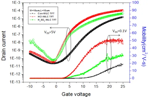
Figure 2. shows the IDS-VGS transfer characteristics and field-effect mobility (μFE) of
H2SO4-NILC TFTs, HCl-NILC TFTs and control-NILC TFTs. It was found that H2SO4
-NILC TFTs and HCl--NILC TFTs have superior electrical characteristics such as high field-effect mobility, low threshold voltage, low subthreshold slope and high on/off
current ratio, especially HCl-NILC TFTs. As showed in TABLE I., the device
parameters were extracted at W / L = 10μm / 10μm. The threshold voltage (VTH)
was defined as the gate voltage required to achieve a normalized drain current of
IDS = (W / L) × 100 nA at VDS = 5 V. The subthreshold slope (S.S.) and the on/off
current ratio were measured at VDS = 5 V, while the μFE was measured at VDS = 0.1 V.
Compared to con-NILC TFTs, the μFE of HCl-NILC TFTs is 172% increased and
on/off current ratio is 387% improved.
Figure 2. Typical IDS-VGS transfer characteristics and field-effect mobility of
H2SO4-TFTs, HCl-TFTs and control-TFTs.
ECS Transactions, 33 (5) 165-168 (2010)
166 ecsdl.org/site/terms_use) unless CC License in place (see abstract). address. Redistribution subject to ECS terms of use (see
140.113.38.11
TABLE I. Average values of the field-effect mobility, threshold voltage, subthreshold
slope, on/off current ratio of TFTs.
In Figure 3., we use Levinson’s and Proano’s method to calculate the trap charge densities (7,8), and the results showed that the Ni trap densities of
HCl-NILC TFT and H2SO4-NILC TFT are 3.61 × 1012 cm-2 and 5.05 × 1012 cm-2
respectively. These values were lower than the control sample which was 7.28 × 10¹²
cm-2. It indicated that the Ni or NiSi2 residuals at the surface of NILC were
reduced effectively after HCl or H2SO4 treatment. That could be the reason for the
electrical characteristics’ enhancement.
Figure 3. The trap charge densities of all samples. They can be estimated from the slope of the linear segment of ln[IDS/(VGS-VFB)] vs. 1/( VGS-VFB )2.
Conclusion
An investigation of poly-Si TFTs using HCl and H2SO4 solution treatment had led to
the development of a simple and effective process to improve the TFT electrical properties. It was found that HCl and H2SO4 solution treatment TFT exhibited higher μFE,
superior S.S., lower VTH, higher on / off current ratio and lower Ni trap state density as
compared with typical NILC TFTs. That was because after chemical solution treatment, the Ni or NiSi2 residuals at the surface of Si were reduced. That could be the reason for
electrical properties enhancement.
ECS Transactions, 33 (5) 165-168 (2010)
167 ecsdl.org/site/terms_use) unless CC License in place (see abstract). address. Redistribution subject to ECS terms of use (see
140.113.38.11
References
1. H. Oshimaand, S.Morozumi, IEDM Tech. Dig., 157 (1989).
2. B. D. Choi, H. S. Jang, O. K. Kwon, H. G. Kim, and M. J. Soh, IEEE Trans.
Consumer Electron., 46(1), 95 (2000).
3. S. W. Lee and S. K. Joo, IEEE Electron Device Lett., 17(4), 160 (1996).
4. Z. Meng, M. Wang, and M. Wong, IEEE Trans. Electron Devices, 47(2), 404 (2000).
5. P. J. van der Zaag, M. A. Verheijen, S. Y. Yoon, and N. D. Young, Appl. Phys. Lett., 81(18), 3404 (2002).
6. S. Y. Yoon, K. H. Kim, C. O. Kim, J. Y. Oh, and J. Jang, J. Appl. Phys., 82(11), 5865 (1997).
7. J. Levinson, G. Este, M. Rider, P. J. Scanlon, F. R. Shepherd, and W. D. Westwood, J. Appl. Phys., 53, 1193 (1982).
8. R. E. Proano, R. S. Misage, and D. G. Ast, IEEE Trans. Electron Devices, 36, 1915 (1989).
ECS Transactions, 33 (5) 165-168 (2010)
168 ecsdl.org/site/terms_use) unless CC License in place (see abstract). address. Redistribution subject to ECS terms of use (see
140.113.38.11
![Figure 3. The trap charge densities of all samples. They can be estimated from the slope of the linear segment of ln[I DS /(V GS -V FB )] vs](https://thumb-ap.123doks.com/thumbv2/9libinfo/7647159.138921/3.918.231.690.437.770/figure-charge-densities-samples-estimated-slope-linear-segment.webp)
