Reduction of Test Power during Test Application in Full-Scan Sequential Circuits with Multiple Capture Techniques
6
0
0
全文
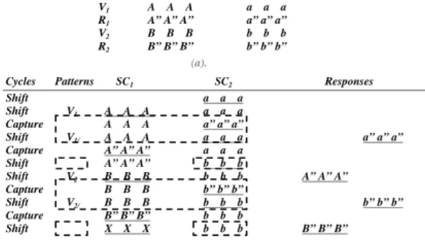
(2) discharging of load capacitance. Generally, the power distribution in a CMOS circuit, the static power dissipation and short-circuit power dissipation contribute up to 20% of the total power dissipation. The remaining 80% is attributed to dynamic power dissipation caused by switching of the gate outputs [4]. Therefore, the dynamic power dissipation takes the dominant part of power consumption for existing CMOS technology. If the gate is part of a synchronous digital circuit controlled by a global clock, it follows that the dynamic power Pd required to charge and discharge the output capacitance load of every gate is given by Pd = 1 / 2 × Cload × V 2 DD / Tcyc × N G. (. ). Where Cload is the load capacitance, VDD is the supply voltage, Tcyc is the global clock period and NG is the total number of gate output transitions (0Æ1 or 1Æ0). The vast majority of power reduction techniques concentrate on minimizing the dynamic power dissipation by reducing one or more variables of Pd. The supply voltage VDD is usually not under designer control and global clock period Tcyc or more generally. Thus, node transition count (NTC) is used as a quantitative measure for power dissipation throughout the paper.. 2.2 Capture Violation Review Capture violation is a mainly problem in multiple capture techniques, when each sub-scan chain captures the responses at different cycles that may cause the data dependence issue. In the following, we use an example to illustrate this problem in details. Figure 1 shows that an example of capture violation scheme, clearly we can to see that there is a data dependence between scan cells S1 and S2 when they capture response at different cycles. For example, if S1 captures response before S2, the test stimulus bit in S1 may change the status and will cause G1 (logic gate 1) become undetected. On the other hand, if S2 captures response before S1, it may change the test stimulus bit in S2 and will cause G2 (logic gate 2) become undetected as well. Therefore, capture violation problem is a key problem for multiple capture techniques.. In this section, we use a simple example to illustrate the test pattern insertion method. In Figure 2, we assume that there is a circuit with 6 scan cells and are grouped into 2 sub-scan chains SC1 and SC2. In Figure 2(a), supposes there are 2 test patterns {V1, V2 : AAA aaa, BBB bbb} will be applied into the circuit, and there are 2 responses {R1, R2: A”A”A” a”a”a”, B”B”B” b”b”b”} will be shifted-out from the circuit. Therefore, in the first step we will shift test pattern V1 {AAA aaa} into SC1 and SC2, and then, sub-scan chain SC2 will be captured first and the value will be replaced from current test pattern {aaa} to captured response data {a”a”a”} simultaneously. In order to avoid capture violation problem for next capture cycle for sub-scan chain SC1, we have to re-shift test pattern value {aaa} into sub-scan chain SC2 before execute the next capture cycle for sub-scan chain SC1; hence a new test pattern V1/ {aaa} will be added behind the V1 {AAA aaa}. Same as above, the test pattern V2/ {bbb} will be also added behind the V2 {BBB bbb} as shown in Figure 2(b). Finally, in order to shift-out the last response data that we have to add an extra test pattern as XXX, the values must be either 111 or 000. We now describe the test pattern insertion rule for our proposed method. The basic idea is to add a test pattern behind each original test pattern as shown in Figure 3. For example, assume that a scan chain is partitioned into n sub-scan chains and there are i original test patterns for circuit testing. Based on the rule of test pattern insertion, we have to add a new test pattern (V1/) behind the original test pattern (V1), which contains the test values of {V1SC , V1SC ,.....V1SC }. After that, 2. 2. 3. n. V1 R1 V2 R2. A A A A” A” A” B B B B” B” B” (a).. Scan Output. S1. S2. Cycles Shift Shift Capture Shift Capture Shift Shift Capture Shift Capture Shift. ….. Pseudo Inputs. G1 ..…. ..…. G2. CUT Primary Inputs. n. patterns will be added into this test set. The draw of the pattern insertion method is that it increase too many test patterns in the test set, thus the test application time will be increased greatly. The following shows the equation of test application cycles by using the pattern insertion method.. Pseudo Outputs Scan Input. 3. another new test pattern (V2/) will be added behind the original test pattern (V2), which contains the test values of {V2 SC ,V2 SC ,.....V2 SC }. Hence, totally there are i new test. Patterns. SC1. V1. A A A A A A A A A A” A” A” A” A” A” B B B B B B B B B B” B” B” X X X. V1/ V2 V2/. SC2 a a a a a a a” a” a” a a a a a a b b b b b b b” b” b” b b b b b b b b b. a a a a” a” a” b b b b” b” b” Responses. a” a” a”. A” A” A” b” b” b” B” B” B”. (b).. Primary Outputs. Figure 2(a) 2 original test patterns. (b) sequence for test pattern insertion.. Figure 1. An example of capture violation scheme.. 3. Proposed Method 3.1 Test Pattern Insertion. - 255 -.
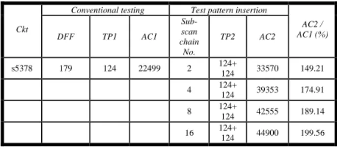
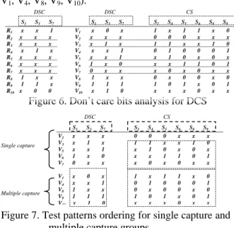
(3) Conventional testing. ……. SC n. V1SC1 V1SC 2 …… V1SC2 …… V2SC1 V2SC2 …… V2SC2 …… V3SC1 V3SC2 …… V3SC2 ……. V1 SC n V1SCn V2 SCn V2 SCn V3SCn V3SCn. SC 1 SC 2. V1 V1/ The inserted test patterns. V2 V2 / V3 V3/. ViSC1 ViSC2 ViSC2. …. …. …. …. Vi Vi /. …… ……. ViSCn ViSCn. ……. Ckt. V1 V2 V3. AAA BBB CCC (a).. AAA BBB CCC. V1 /. V V V. 2. BBB. 2 /. CCC. AAA. AAA. AAA. AAA. BBB. BBB. BBB. BBB. CCC. CCC. CCC. CCC. AC1. 179. 124. 22499. AC2 / AC1 (%). 149.21 174.91 189.14 199.56. Table 1: Test application time overhead for s5378. 3.2 Scan Chain Partition. Test Application Cycles = (DFF + (DFF-SC1_DFF) + n) × i + SC1_DFF (1) DFF: Scan shift cycles for each original test pattern. DFF-SC1_DFF: Scan shift cycles for each new test pattern. n: Capture cycles for each test pattern testing. i: The number of original test patterns. SC1_DFF: Last scan shift cycles. For example, we assume that there is a circuit with 9 scan cells and divide into 3 sub-scan chains. In Figure 4 (a), there are 3 test patterns {V1 – V3 : AAAAAAAAA, BBBBBBBBB, CCCCCCCCC} will be applied into this circuit, based on the test pattern insertion rule in Figure 3 that we can follow the procedure to generate the new test patterns as V1/ {AAA, AAA}, V2/ {BBB, BBB}, and V3/ {CCC, CCC}. Based on this rule, we can get the new test pattern set as shown in Figure 4(b), and the total number of increased patterns are 3 since i = 3. Hence, there are 3 test patterns will be added into original test set, and the total test application cycle is 57 ((9 + ( 9 - 3) + 3) × 3 + 3). Compared to conventional testing ((9 + 1) × 3 + 9 = 39), the proposed test pattern insertion method will take more 46.15% (57/39 - 1)%) test application cycles than conventional testing, the overhead of test application time is too much for this method. As the test application time overhead of circuit s5378 showed in Table 1, the test application time will be increased 49.21%, 74.91%, 89.14% and 99.56%, respectively, when 2, 4, 8 and 16 sub-scan chains are used. SC 1 SC 2 SC 3 AAA. TP1. s5378. Figure 3. The rule of test pattern insertion. V1. DFF. Test pattern insertion Subscan TP2 AC2 chain No. 124+ 2 33570 124 124+ 4 39353 124 124+ 8 42555 124 124+ 16 44900 124. Generally, there are many test cubes, i.e., test patterns and response data with don’t care bits, which are usually generated by ATPG tool. Our basic idea is to analyze the don’t care response bits and divide the scan cells into two sub-scan chains, which are don’t care bit sub-scan chain(DCS) and care bit sub-scan chain(CS). For next, we use a simple example in Figure 5 to illustrate our basic idea. We assume that there is a response date set with don’t care bits as showed in Figure 5(a), after the response data set is analyzed, we can obtain that there are 3 scan cells (S1, S3, S7,) contain over 7 don’t care bits if we perform a third of scan cells in the don’t care bit sub-scan chain(DCS). Hence, the scan cells S1, S3 and S7 will be put into DCS and others will be put into CS. The scan cell number of DCS and DS are 3 and 6, respectively. The partitioned sub-scan chain architecture is shown in Figure 5(b). R1 R2 R3 R4 R5 R6 R7 R8 R9 R10. S1 x x x x x x x 1 1 x 8. S2 0 x 1 x 0 x 0 x 1 1 4. S3 x x 1 x x x x x 1 0 7. S4 1 0 1 0 x x x 1 1 x 4. S5 x x 1 1 1 x 0 0 0 x 4. S6 1 0 x 0 0 1 x 0 1 x 3. S7 1 x x x x x x x x 0 8. S8 0 x 1 x 1 0 1 x 0 1 3. S9 1 x 0 1 x 1 1 0 1 0 2. Figure 5(a). A response data set with don’t care bits DSC R1 R2 R3 R4 R5 R6 R7 R8 R9 R10. S1 x x x x x x x 1 1 x. S3 x x 1 x x x x x 1 0. DC S7 1 x x x x x x x x 0. S2 0 x 1 x 0 x 0 x 1 1. S4 1 0 1 0 x x x 1 1 x. S5 x x 1 1 1 x 0 0 0 x. S6 1 0 x 0 0 1 x 0 1 x. S8 0 x 1 x 1 0 1 x 0 1. S9 1 x 0 1 x 1 1 0 1 0. Figure 5(b).The sub-scan chain architecture after partition. 3.3 Test Pattern Ordering. (b).. Figure 4 (a) Original test patterns (b) Test patterns after test pattern insertion. After the sub-scan chain DCS is identified, we have to further analyze that how many response data in DCS are all with don’t care response bit, it means that these corresponding patterns can skip the capture operation. - 256 -.
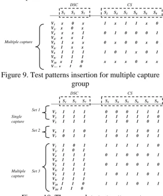
(4) for DSC during testing. In Figure 5(b), there are 3 scan cells in sub-scan chain DCS, and there are 5 response data(R2, R3, R5, R6, R7) are all with don’t care bits in DCS, thus we can skip the capture operation for sub-scan chain DCS during these corresponding test pattern(V2, V3, V5, V6, V7) in testing. The analysis result is shown in Figure 6. Based on the analysis results, we have to order the corresponding patterns and divide them into two groups as showed in Figure 7, which are single capture and multiple capture groups. The single capture group contains 5 test patterns (V2, V3, V5, V6, V7) and the multiple capture group contains another 5 test patterns (V1, V4, V8, V9, V10). DSC R1 R2 R3 R4 R5 R6 R7 R8 R9 R10. S1 x x x x x x x 1 1 x. S3 x x x 1 x x x x 1 0. DSC S7 1 x x x x x x x x 0. V1 V2 V3 V4 V5 V6 V7 V8 V9 V10. S1 x x x x x 1 0 1 1 x. S3 0 x 1 x x x x x 1 1. CS S7 x x x 1 1 0 x x 1 0. S2 1 0 1 0 x x x 0 1 x. S4 x 0 1 1 1 x 0 x 0 x. S5 1 0 x 0 0 1 x 0 1 x. S6 1 x x 0 x 1 0 0 x 0. S8 x x 1 0 0 0 x x 0 x. S9 0 x 0 1 x 1 x 0 1 x. Figure 6. Don’t care bits analysis for DCS DSC. Single capture. Multiple capture. CS. V2 V3 V5 V6 V7. S1 x x x 1 0. S3 x 1 x x x. S7 x x 1 0 x. S2 0 1 x x x. S4 0 1 1 x 0. S5 0 x 0 1 x. S6 x x x 1 0. S8 x 1 0 0 x. S9 x 0 x 1 x. V1 V4 V8 V9 V10. x x 1 1 x. 0 x x 1 1. x 1 x 1 0. 1 0 0 1 x. x 1 x 0 x. 1 0 0 1 x. 1 0 0 x 0. x 0 x 0 x. 0 1 0 1 x. (DFF+1): Scan shift cycles for all scan cells and plus one capture cycle for CS. (Set2_TP): The test pattern number of Set2. Based on the above explanation, Set1 takes the test application time less than conventional circuit testing, and Set2 equals. In other words, if we can obtain more test patterns in Set1 that the test application time can be reduced more efficiently. Therefore, we approach another method to add Set1 size is to determine 0’s or 1’s for don’t care bits. We now use example in Figure 8(a) again, there are 4 Set2 test patterns (V3:x1x, V5 :xx1 , V6:1x0, V7:0xx) in DCS, we first assigning 0 into the don’t care bits, and we can get results as V3:010, V5 :001 , V6:100, V7:000. After that, we find that there is a test pattern (V7:000) can be moved from Set2 to Set1. Secondary, let us assigning 1 into the don’t care bits, and get results as V3:111, V5:111 , V6:110, V7:011, we find that there are 2 test patterns (V3:111, V5 :111) can be moved from Set2 to Set1. Hence, assigning 1 for don’t care bit is better than assigning 0 for don’t care bit on this case. Figure 8(b) shows that Set1 and Set2 structure after the don’t care bits are assigned to 1. However, the determined test patterns can reduce the test application time more efficiently than before, because the Set1 size is increased from 1 to 3 patterns. DSC. Set 1 Set 2. Figure 7. Test patterns ordering for single capture and multiple capture groups Consider for single capture group. Some of test patterns in DSC may all with don’t care bits. If so, these patterns can put into same test set called “Set1”, and other patterns put into another set called “Set2”. For our example showed in Figure 8(a), after the single capture group is divided that Set1 contains one test pattern(V2) and Set2 contains 4(V3, V5, V6, V7) test patterns, respectively. For Set1, we shift the test pattern into both sub-scan chain DCS and CS for one time only, and next, we just shift patterns into CS for capture operation because Set1 contains same test data for DCS. The equation of test application cycles for Set1 as follows: Test Application Cycles = (DFF+1) + ((CS_DFF+1) × (Set1_TP-1)) … (2) (DFF+1): First scan shift cycles for all scan cells and plus one capture cycle for CS. (CS_DFF+1): Scan shift cycles and plus one capture cycle for CS. (Set1_TP-1): The test pattern numbers of Set1, decrease one test pattern for first test pattern. For Set2, each test pattern has to shift into both sub-scan chains DCS and CS, and plus a capture cycle for sub-scan chain CS. The equation of test application cycles for Set2 as follows: The Application Cycles = (DFF+1) × Set2_TP…. (3). CS. V2. S1 x. S3 x. S7 x. S2 0. S4 0. S5 0. S6 x. S8 x. S9 x. V3 V5 V6 V7. x x 1 0. 1 x x x. x 1 0 x. 1 x x x. 1 1 x 0. x 0 1 x. x x 1 0. 1 0 0 x. 0 x 1 x. (a) CS. DSC. Set 1 Set 2. V2 V3 V5. S1 1 1 1. S3 1 1 1. S7 1 1 1. S2 0 1 1. S4 0 1 1. S5 0 1 0. S6 1 1 1. S8 1 1 0. S9 1 0 1. V6 V7. 1 0. 1 1. 0 1. 1 1. 1 0. 1 1. 1 0. 0 1. 1 1. (b). Figure 8(a).Divide the single capture group into Set1 and Set2. (b).The test set of Set1 and Set2 after assigning 1to don’t care bits. For next, let us consider for the multiple capture group. We have to follow the test pattern insertion rule as mentioned in section 3.1 to generate a test set called Set3, which is shown in Figure 9. For the test application time calculation, Set3 will take more test application cycles than Set1 and Set2 because there are many test patterns are inserted into original multiple capture group. The equation of test application cycles for Set3 as follows: The Application Cycles = ((DFF+DCS_DFF+2)× Set3_Org_TP) + CS_DFF ……………….. (4) (DFF): Scan shift cycles for each original test pattern. (DC_DFF): Scan shift cycles for each new test pattern. (+2): Two capture cycles for DCS and CS. (Set3_Org_TP): The number of original test patterns. (DCS_DFF): Last scan shift cycles. Finally, we have to assigning 1 for all the don’t care bits because it can add the Set1 size, and we can get a. - 257 -.
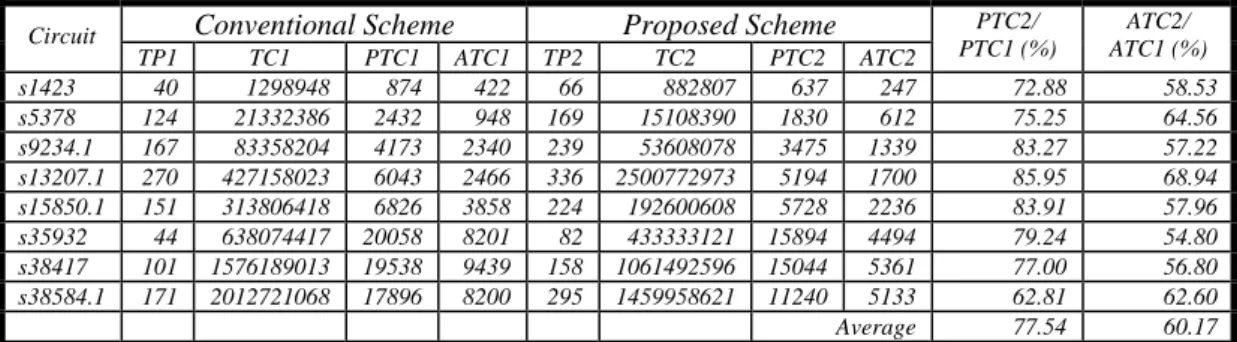
(5) complete test set as showed in Figure 10, this test set contains 3 test patterns in Set1, 2 test patterns in Set2 and 8 test patterns in Set3. DSC S1 V1 V1/ V4 V4/ V8 V8/ V9 V9/ V10 V10/. Multiple capture. x x x x 1 1 1 1 x x. CS. S3. S7. S2. S4. S5. S6. S8. S9. 0 0 x x x x 1 1 1 1. x x 1 1 x x 1 1 0 0. 1. x. 1. 1. x. 0. 0. 1. 0. 0. 0. 1. 0. x. 0. 0. x. 0. 1. 0. 1. x. 0. 1. x. x. x. 0. x. x. Figure 9. Test patterns insertion for multiple capture group DSC S3. S7. S2. S4. S5. S6. S8. S9. Set 1. V2 V3 V5. 1 1 1. 1 1 1. 1 1 1. 0 1 1. 0 1 1. 0 1 0. 1 1 1. 1 1 0. 1 0 1. Set 2. V6 V7. 1 0. 1 1. 0 1. 1 1. 1 0. 1 1. 1 0. 0 1. 1 1. V1 V1/ V4 V4/ V8 V8/ V9 V9/ V10 V10/. 1 1 1 1 1 1 1 1 1 1. 0 0 1 1 1 1 1 1 1 1. 1 1 1 1 1 1 1 1 0 0. 1. 1. 1. 1. 1. 0. 0. 1. 0. 0. 0. 1. 0. 1. 0. 0. 1. 0. Single capture. Multiple capture. CS. S1. Set 3. 1. 0. 1. 1. 0. 1. 1. 1. 1. 0. 1. 1. Figure 10. The complete test pattern set. 3.4 The Proposed Architecture The basic architecture of our proposed method is shown in Figure 11, the scan chain is divided into DCS and CS sub-chains, and only one sub-scan chain will be enabled at a time during scan shift or capture operations. In the normal mode, the signal SE will be set to 0, and the signals CLK_DCS and CLK_CS are mapped to system clock. Thus all scan cells are activated in the normal condition. There are 2 types of cycles in the test mode, which are scan shift cycle and capture cycle. During test mode, the signal SE will be set to 1 and 0 for scan shift cycle and capture cycle, respectively. Besides, the signals CLK_DCS and CLK_CS will be activated for sub-scan chains DCS and CS during scan shift or capture operations. COMBINATIONAL BLOCK. SI. 5. Conclusions. SO DCS. power reduction. In this experimental, the test patterns are generated by Sytest ATPG tool “Turboscan”. Table 2 shows the experimental results of test application time overhead. The circuit name is shown in column 1. After the circuit name, the follow 3 columns “DFF”, “TP1” and “AC1” give the number of flip-flops, the number of test patterns and the number of test application cycles for conventional scan test method, respectively. After that, the latter columns are defined for our proposed scheme. Columns “DCS_DFF” and “CS_DFF” give the flip-flop number of sub-scan chain DCS and sub-scan chain CS. The number of test patterns for Set1, Set2 and Set3 are shown in columns “TP2_Set1”, “TP2_Set2” and “TP2_Set3, respectively. Column “AC2” gives the number of test application cycles. And then, column “1 or 0” stand for assigning 1 or 0 for don’t care bits. The last column gives the result of test application time overhead. In this experimental, the increased test patterns of Set3 may increase the test application time. However, as the results show, for circuit such as s13207.1, the number of test application cycles of the proposed method is smaller than the conventional testing. It means that if we can get bigger size for test pattern set Set1, we may get a smaller test application time than the conventional testing. The experimental results for power dissipation are shown in Table 3. Same as in Table 2, the circuit name is also shown in column 1, and the following 4 columns are defined for conventional scheme results. Columns “TP1” and “TC1” give the number of test patterns and the number of total transition counts. The maximum number of transition counts and average number of transition counts are shown in columns “PTC1” and “ATC1”, respectively. For the latter columns, they are defined for our proposed scheme results. In columns “TP2” and “TC2”, the number of test patterns and the number of total transition counts are given. And then, the columns “PTC2” and “ATC2” give the maximum number of transition counts and average number of transition counts, respectively. Finally, the last 2 columns are shown for the reduction results of maximum and average node transition counts. As this experimental results show, our proposed method can reduce maximum node transition counts and average node transition counts by 22.46% and 39.83% in average, respectively.. CS. SE CLK_C. CLK_DCS (a). Figure 11. The proposed architecture. 4. Experimental Results The proposed method is implemented on eight largest ISCAS89 benchmark circuits, and used the node transition count (NTC) to estimate the percentage of. For multiple capture technique, it has often caused some side effects in order to deal with capture violation problem, either requires large hardware overhead to cause performance degradation or increase test application time. However, the proposed approach can reduce the peak power as well as average power dissipation during scan shift and capture operations, without requiring large hardware overhead. In addition, the proposed approach is very simple and easy to implement for any large full-scan sequential circuits without impacting the fault coverage.. - 258 -.
(6) Conventional Scheme Circuit s1423 s5378 s9234.1 s13207.1 s15850.1 s35932 s38417 s38584.1. DFF. TP1. AC1. 74 179 211 638 534 1728 1636 1426. 40 124 167 270 151 44 101 171. 3074 22499 35615 173168 81319 77804 166973 245443. Proposed Scheme DCS DFF 21 59 71 211 182 546 553 462. CS_ DFF 53 120 140 427 352 1182 1083 964. TP2_ Set1. TP2_ Set2. TP2_ Set3. AC2. 4 9 11 188 47 4 1 40. 10 70 84 16 31 2 43 7. 26+26 45+45 72+72 66+66 73+73 38+38 57+57 124 +124. 3562 24668 40018 147492 86124 96406 197998 284375 Average. 1 or 0 0 1 1 0 1 1 1 1. AC2 / AC1 (%) 115.88 109.64 112.36 85.17 105.91 123.91 118.58 115.86 110.91. Table 2: Experimental results of test application time overhead. Conventional Scheme. Circuit s1423 s5378 s9234.1 s13207.1 s15850.1 s35932 s38417 s38584.1. TP1 40 124 167 270 151 44 101 171. TC1 1298948 21332386 83358204 427158023 313806418 638074417 1576189013 2012721068. PTC1 874 2432 4173 6043 6826 20058 19538 17896. ATC1 422 948 2340 2466 3858 8201 9439 8200. Proposed Scheme TP2 66 169 239 336 224 82 158 295. TC2 882807 15108390 53608078 2500772973 192600608 433333121 1061492596 1459958621. PTC2 637 1830 3475 5194 5728 15894 15044 11240. ATC2 247 612 1339 1700 2236 4494 5361 5133 Average. PTC2/ PTC1 (%) 72.88 75.25 83.27 85.95 83.91 79.24 77.00 62.81 77.54. ATC2/ ATC1 (%) 58.53 64.56 57.22 68.94 57.96 54.80 56.80 62.60 60.17. Table 3: Experimental results for peak and average power reduction. References [1]. [2]. [3]. [4]. [5]. [6]. [7]. [8]. P. Girard, “Survey of Low-Power Testing of VLSI Circuits”, IEEE Design & Test of Computers, vol. 19, no. 3, pp. 82-92, 2002. Y. Bonhomme, P. Girard, C. Landrault, S. Pravossoudovitch, “Test Power: a Big Issue in Large SOC Designs”, IEEE Test and Applications (DELTA’02), 2002. Y. Zorian, “A Distributed BIST Control Scheme for Complex VLSI Devices”, Proc. VLSI Test symp., pp. 4-9, 1993. CHANDRAKASAN, A.P., and BRODERSEN, R.W.: “Low power digital CMOS design”, Kluwer Academic Publishers, 1995. P. Girard, C. Landrault, S. Pravossoudovitch and D.Severac , “Reducing Power Consumption during Test Application by Test Vector Ordering”, IEEE, 1998. P. Girard, L. Guiller, C. Landrault, and S. Pravossoudovitch, “A Test Vector Ordering Technique for Switching Activity Reduction during Test Operation”, in Proc. 9th Great Lakes Symp. VLSI, Mar. 1999, pp.24-27. M. Bells, D. Bakalis and D. Nikolos, “Scan Cell Ordering for Low Power BIST”, Proc. IEEE Computer Society Annual Symposium, Feb. 2004, pp.281-284. Y. Bonhomme, P. Girard, C. Landrault, and S. Pravossoudovitch, “Power Driven Chaining of Flip-flops in Scan Architectures”, Proc. of Int’l Test Conf., 2002, pp. 796-802.. [9] TC. Huang, KJ. Lee, “Reduction of power consumption in scan-based circuits during test application by an input control technique”, IEEE Transaction computer Aided Design of IC and Systems, Vo1.20, No.7, July 2001, pp. 911-917. [10] N. Nicolici, B.M. AL-Hashimi, A.C. Williams, “Minimization of power dissipation during test application in full-scan sequential circuits using primary input freezing”, IEEE Proc. Computer. Digit.Tech, Vo1.147, No.5, September 2000, pp. 313-322. [11] Ranganathan Sankaralingam, Bahram Pouya, Nur A. Touba, “Reducing Power Dissipation Test Using Scan Chain Disable”, IEEE, 2001. [12] Nadir Z. Basturkmen, Sudhakar M. Reddy, Irith Pomeranz, “A Low Power Pseudo- Random BIST Tehnique”, IEEE, (IOLTW’02). [13] Paul M. Rosinger, Bashir M. Al-Hashimi, Nicola Nicolici, “Scan Architecture for Shift and Capture Cycle Power Reduction”, IEEE, (DFT’02). [14] Y. Bonhomme, P. Girard, L. Guiller, C. Landrault, S. Pravossoudovitch, “A Gated Clock Scheme for Low Power Scan Testing of Logic ICs or Embedded Cores”, IEEE Asian Test Symp., November 2001.. - 259 -.
(7)
數據
+2
相關文件
Field operators a † ↵, (q) and a ↵, (q) create or destroy a photon or exciton (note that both are bosonic excitations) with in-plane momentum q and polarization (there are
Though there’s a growing trend of employing famous Hollywood actors to voice characters in order to provide movies with star power, there are still many unknowns but
Unless prior permission in writing is given by the Commissioner of Police, you may not use the materials other than for your personal learning and in the course of your official
It is useful to augment the description of devices and services with annotations that are not captured in the UPnP Template Language. To a lesser extent, there is value in
• Learn strategies to answer different types of questions.. • Manage the use of time
- - A module (about 20 lessons) co- designed by English and Science teachers with EDB support.. - a water project (published
There is no general formula for counting the number of transitive binary relations on A... The poset A in the above example is not
There are thirty students in the classroom.. Please be
![TraditionalMLCalgorithmsmainlytacklethebatchMLCproblem,wheretheinputdataarepresentedinabatch[24,28].Nevertheless,inmanyMLCapplicationssuchase-mailcategorization[22],multi-labelexamplesarriveasastream.Onlineanalysisistherefore dimensionreducermotivatedbyma](data:image/gif;base64,R0lGODlhAQABAIAAAP///wAAACH5BAEAAAAALAAAAAABAAEAAAICRAEAOw==)