Z掃瞄量測氧化鋅薄膜之非線性光學效應
48
0
0
全文
(2) Z-掃瞄量測氧化鋅薄膜之非線性光學效 應 Z-scan measurement of optical nonlinearities of ZnO thin film. 研 究 生 :鄭 介 任. student:Chieh-Jen Cheng. 指導教授 :張 振 雄. Advisor:Dr. Chen-Shiung Chang Dr. Wen-Feng Hsieh. 國 立 交 通 大 學 光 電 工 程 研 究 所 碩 士 論 文 A Thesis Submitted to Institute of Electro-Optical Engineering College of Electrical Engineering and Computer Science National Chiao Tung University In Partial Fulfillment of the Requirements for the Degree of Master in Electro-optical Engineering June 2003 Hsin-chu,Taiwan,Republic of China 中 華 民 國 九 十 二 年 六 月.
(3) Z-掃瞄量測氧化鋅薄膜之非線性光學效應. 研究生:鄭介任. 指導教授:張振雄 教授 謝文峰 教授. 國立交通大學光電工程研究所 摘要. 利用飛秒超短脈衝鈦藍寶石雷射從事變化強度 Z-掃瞄量測技術 研究 Laser-MBE 磊晶成長之氧化鋅薄膜。在 742nm,其雙光子吸收 係數 β = 1905 cm/GW,三階非線性折射係數 γ =2.2×110-11 cm2/W 以 及五階非線性折射係數 σr = 4.51×10⁻²⁰ cm3,比理論預測大了許多。 而由變化波長的掃瞄結果顯示出,非線性吸收及折射增強的原因是由 於入射光的能量接近雙光子共振能帶。激子共振現象也會對非線性折 射有很大的貢獻,這是由於自由激子受到強光的激發而產生自由載子 影響了非線性效應,使得非線性效應大幅增強。. I.
(4) Z-scan measurement of optical nonlinearities of ZnO thin film Student: Chieh-Jen Cheng. Advisor: Dr. Chen-Shiung Chang Dr. Wen-Feng Hsieh. Institute of Electro-Optical Engineering National Chiao Tung University. Abstract By utilizing femtosecond Kerr Mode-Locked Ti:Sapphire laser as Z-scan light source, we have studied intensity dependent nonlinear optical properties of ZnO thin film growth by Laser-MBE epitaxy.. The two photon absorption coefficient β = 1905. cm/GW, nonlinear refractive index γ = 2.11×10⁻¹¹cm2/W and fifth order nonlinear refractive index σr = 4.51×10⁻²⁰cm3 with 748nm-wavelength of incident laser. Compared with two-band model, γ is 2000 times larger than theoretical value and this owes to near two-photon resonance. Results of β dependent with wavelength of incident light reveal this two-photon resonance behavior and results of σr dependent with wavelength of incident light show that free-carriers are induced by free-excitons under intense light sources pumping.. The results of γ dependent with wavelength of. incident light also show two-photon resonance behavior and excitonic enhancement.. II.
(5) Table of Contents Abstract (in Chinese)… … … … … … … … … … … … … … … … … … … … I Abstract (in English) … … … … … … … … … … … … … … … … … … … … II Acknowledgements… … … … … … … … … … … … … … … … … … … … ..III Contents… … … … … … … … … … … … … … … … … … … … … … … … … IV List of Figures… … … … … … … … … … … … … … … … … … … … … … ..VI List of Tables… … … … … … … … … … … … … … … … … … … … … … ...VII Chapter 1 Introduction… … … … … … … … … … … … … … … … … … .1 1-1 Background… … … … … … … … … … … … … … … … … … … … … … ..2 1-1-1 Ultrafast all-optical switching… … … … … … … … … … … ...... 2 1-1-2 Optical limiting… … … … … … … … … … .… … … … … … … … ..3 1-1-3 effective χ(3) by cascade χ(2):χ(2)… … … … … … … … … … … … . 3 1-2 Review of χ(3) measurement… … … … … … … … … … … … … … .........4 1-2-1 Four-wave mixing… … … … … … … … … … … … … … … … … .. 4 1-2-2 Z-scan … … … … … … … … … … … … … … … … … … … … … … .5 1-2-3 Excite-probe Z-scan… … … … … … … … … … … … … … … … … 7 1-3 Merits of ZnO… … … … … … … … … … … … … … … … … … … … … ...9 1-4 Aim of this research… … … … … … … … … … … … … … … … … … … ..9 Chapter 2 Theoretical background… … … … … … … … … … … … .11 2-1 Analysis of Z-scan… ..… … ..… … … … … … … … … … … … … … … ..12 2-1-1 Bound-electronic and Free-carrier nonlinearity… ..… ..… … … 12 2-2 Coefficients of nonlinear absorption and refraction… … … … ..… … .18 2-3 Dispersion of bound-electronic nonlinearities: Two-Band Model..14 2-3-1 Nonlinear absorption… … … … … … … … … … … … … … … … .14 2-3-2 Nonlinear refraction… … … … … … … … … … … … … … … … ..15 Chapter 3 Experiments … … … … … … … … … … … … ...… … … … .19 3-1 XRD analysis of ZnO thin film growth by Laser MBE… … … … … .19 3-2 Photoluminescence and transmission spectra… … … … … … … … ....19 3-3 Single beam Z-scan apparatus… … … … … … … … … … … … … … … 20 IV.
(6) Chapter 4 Results and Discussions… … … … … … … … … … … ...22 4-1 XRD… … … … … … … … … … … … … … … … … … … … … ..… … … .22 4-2 Photoluminescence Spectra… … … … … … … … … … … … … … … … 23 4-3 Transmission Spectra … … … … … … … … … … … … … … … … … … .24 4-4 Measurement of Z-scan… … … … … … … … ..… … … … … … … … … 24 Chapter 5 Conclusions and Perspectives… … … … … … … … … 36 5-1 Conclusions… … … … … … … … … … … … … … … … … … … … … … 36 5-2 Perspectives… … … … … … … … … … … … … … … … … … … … … … 37 References… … … … … … … … … … … … … … … … … … … … … … … 39. V.
(7) List of Figures Fig. 1-1 Ratio of n2/kβ as a function of hω/Eg Fig. 1-2 DFWM geometry to allow temporal dynamics measurements Fig. 1-3 Z-scan geometry Fig. 1-4 Predicted Z-scan signal for positive and negative nonlinear phase shifts Fig. 1-5 Optical geometry for a two-color Z-scan Fig. 3-1 Sketch diagram of photoluminescence spectra Fig. 3-2 The Z-scan apparatus Fig. 4-1 Result of X-ray diffraction measurement Fig. 4-2 Result of Photoluminescence spectra measurement. 2 5 6 7 8 19 21 22 23. Fig. 4-3 Result of transmission spectra measurement. 24. Fig. 4-4 (a) Open-aperture Z-scan trace of ZnO. 26. Fig. 4-4 (b) Closed aperture Z-scan trace. 26. Fig. 4-5 The divided result with different pulse intensity Fig. 4-6 Measured TPA coefficients plotted as a function of I0. 28 29. Fig. 4-7 ∆n directly derived from ∆Tp-v plotted as a function of I0 for ZnO Fig. 4-8 Measured TPA coefficients versus irradiance and ∆n/I0 Fig. 4-9 Measured TPA coefficients versus wavelength λ Fig. 4-12 Measured nonlinear refractive index versus wavelength λ Fig. 4-11 Measured nonlinear refractive index versus h? /Eg. 29 31 32 33 34. Fig. 4-12 Measured free-carrier nonlinearity versus wavelength λ. 34. VI.
(8) List of Tables Table I Contributions to the nonlinear absorption spectral function F2 Table II The nondegenerate dispersion function for n2. 15 17. Table III Fitting results of division of Z-scan. 35. VII.
(9) Chapter 1. Introduction. The nonlinear optical properties of semiconductors, used for a variety of applications, are the first studied by Braunstein R et al. [1] and extensively investigated [2].. Some of the. largest nonlinearities have ever been reported in semiconductors [3] and involve near-gap excitation.. However, these resonant nonlinearities, by their nature, involve significant linear. absorption, which is undesirable in many applications.. The nonlinear optical behavior in the. transparency region of solids due to the anharmonic response of bound valence electrons has been studied extensively in the past [4]. Nonlinear refraction associated with this process is known as the bound-electronic Kerr effect.. It is described by a change of refractive index. △n = n2I, where I is the light irradiance (W/cm2) and n2(cm2/W) is the optical Kerr coefficient of the solid.. This type of nonlinearity results from virtual intermediate transitions. [5] as opposed to real intermediate transitions that occur in resonant (electron-hole plasma) nonlinearities. In the language of quantum mechanics, a virtual carrier lifetime can be defined from the uncertainty principle as 1/ω-ωg.. Here, ω is the optical frequency, and ωg = Eg/h, where Eg. is the band-gap energy of the solid, and h is Planck’s constant. This equality means that in the transparency region where ω << ωg, the response time is very fast (<< 10-14 s) and can be regarded as essentially instantaneous. This ultrafast response time has been exploited in applications such as soliton propagation in glass fibers [6] and in the generation of femtosecond pulses in solid-state lasers (Kerr lens mode locking) [7]. Another significant application is the development of ultrafast all-optical-switching (AOS) devices [8]. Although much progress has been made in this area, development of a practical switch has been hindered by the relatively small magnitude of bound-electronic nonlinearities.. -1-.
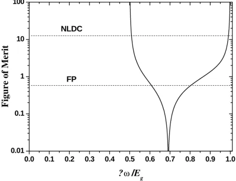
(10) 1-1 Background 1-1-1 Ultrafast all-optical switching One of the applications of ultrafast nonlinear refraction is in the role of all-optical switching.. In order to obtain switching, the required nonlinear phase shift must be achieved. before losses reduce the irradiance.. For the transparent spectral region beneath the. one-photon band gap in semiconductor and for the high irradiances required for ultrafast nonlinear refraction, the dominant loss mechanism is usually two-photon absorption. In order to obtain all-optical switching, the figure of merit (FOM) n2/βλ (where β is the two-photon absorption coefficient) must exceed some critical value; this value depends on the device geometry but is always of the order of unity [9].. The two horizontal lines in Fig. 1-1. represent the minimum acceptable FOM for nonlinear directional couplers (NLDC) and Fabry-Perot (FP) interferometers.. Although it demands a larger FOM, the NLDC scheme is. the preferred practical geometry.. From Fig. 1-1 we see that the FOM requirement is satisfied. either just below the 2PA edge or very near resonance ( hω ˜ Eg ). Since n2 ∝ Eg -4, a low switching threshold at a given wavelength demands a material with the smallest possible band-gap energy. The theory then suggests that the ideal operating region is just below the band gap. 100. NLDC. Figure of Merit. 10. 1. FP. 0.1. 0.01 0.0. 0.1. 0.2. 0.3. 0.4. 0.5. 0.6. 0.7. 0.8. 0.9. 1.0. ? ω /Eg Fig. 1-1 Ratio of n2/kβ (switching parameter or figure of merit) as a function of hω/Eg. The solid line is predicted from the two-parabolic-band model. NLDC stands for nonlinear directional coupler, and FP stands for Fabry-Perot etlon. -2-.
(11) 1-1-2 Optical limiting A passive optical limiting uses a material’s nonlinear response to block the transmittance of high-irradiance light while allowing low-irradiance light to be transmitted (an operation similar to that of photochromic sunglasses). The primary application of optical limiting is to protect sensitive optical components from being damaged by the high-intensity input light. The ideal optical limiter has a high linear transmission for low inputs (e.g., energy), a variable limiting input energy, and a large dynamic range defined as the ratio of the linear transmittance to the minimum transmittance obtained for high input (prior to irreversible damage). Since a primary application of optical limiting is to protect sensors, and fluence (energy per unit area) almost always determines damage to detectors; this is the quantity of interest for the output of a limiter.. 1-1-3 Effective χ. (3). by cascaded second-order effect. There has recently been a growing interest in a phenomenon known as cascading of second-order nonlinearities to obtain large, intensity-dependent phase distortions in optical beams. This phenomenon can be briefly described as follows: when a beam propagates in a medium with a χ(2) nonlinearity out of phase matching, part of the generated second harmonic is converted back to the fundamental frequency, in phase quadrature with respect to the original wave.. There is therefore a phase shift on the fundamental frequency beam. proportional to its intensity, as in a medium with a χ(3) nonlinearity (Kerr medium). Depending on the phase mismatch, the equivalent χ(3) can be positive or negative, corresponding to a self-focusing or a self-defocusing medium.. Although the effect has been. known for a very long time [10], its potentiality of generating large third-order nonlinearities of controllable sign has been exploited just recently [11].. The applications of cascaded. second-order nonlinearities have all-optical switching in waveguides [12], the generation of spatial solitons in quadratic media [13] and mode-locking of lasers [14]. -3-.
(12) 1-2 Review of χ(3) measurement Several experimental techniques are available for measuring the bound-electronic nonlinear response of semiconductors, ie., β and n2.. These measurements include: degenerate. four-wave mixing (DFWM) and Z-scan [15] along with its derivatives [16][17].. 1-2-1 Four-wave mixing Four-wave mixing, where three beams are input to a material and a fourth wave (beam) is generated, can be used for determining the magnitude of material’s nonlinear response and its response time.. If the response is known to be third-order and ultrafast, can be determined. along with some of its symmetry properties by varying the relative polarizations of the input beams (as well as by monitoring the polarization of the fourth wave). In addition, the frequencies of the input beams can be changed independently to determine the frequency dependence of the nonlinear response, but this can result in the need for a complex geometry to satisfy phase-matching requirements. Equal frequencies are often used, resulting in a much simpler geometry for phase matching, and this is referred to as degenerate four-wave mixing (DFWM).. Fig. 1-2 shows one simple geometry for DFWM where two of the input. beams (the forward and backward pumps) are oppositely directed.. If these beams are nearly. plane waves (i.e., well collimated), this geometry ensures phase matching for any third input beam (the signal).. Introducing delay arms into each of the beams also allows the temporal. dynamics of the nonlinearities to be measured for short optical input pulses. A particularly useful measurement is to monitor the energy of the fourth beam (so-called phase-conjugate beam) as a function of the time delay of the perpendicularly polarized backward pump (signal and forward pump have the same linear polarization) [18]. One of the difficulties in the interpretation of DFWM data for third-order nonlinearities is -4-.
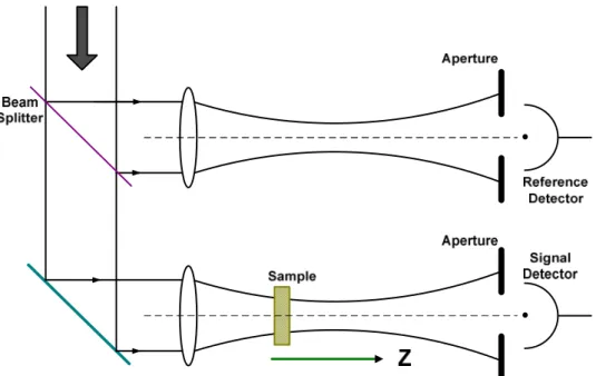
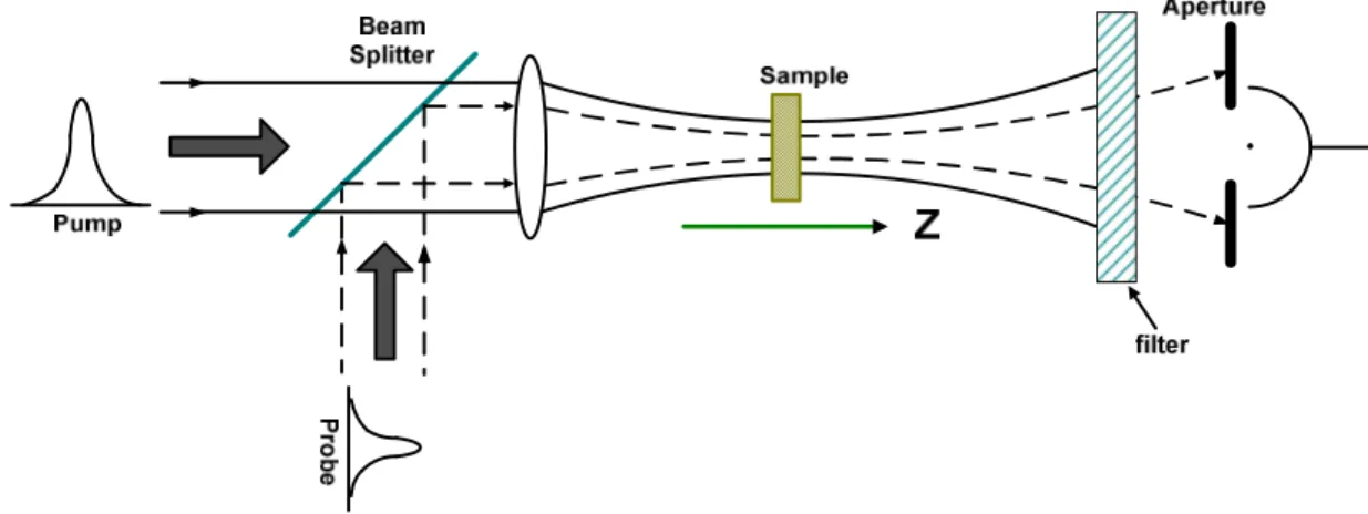
(13) 2. 2. 2. that the signal is proportional to χ (3) = Re{χ (3) } + Im{χ (3) } , and so 2PA and n2 both contribute. Separating the effects is difficult without performing additional experiments. Higher-order nonlinearities also can contribute, making separation of absorptive and refractive effects difficult.. Fig. 1-2 DFWM geometry to allow temporal dynamics measurements. Detector D2 monitors the conjugate beam energy.. 1-2-2 Z-scan Z-scan was developed for measuring nonlinear refraction (NLR) and determining its sign by Sheik-Bahae et al. [19]. It was soon realized that it also was useful for measuring nonlinear absorption (NLA) and separating the effects of NLR from NLA. scan setup is depicted in Fig. 1-3.. A single beam Z. The transmittance of a sample in the far field is measured. through an aperture (Z-scan) or around an obscuration disk (EZ-scan).. The transmittance is. determined as a function of the sample position Z measured with respect to the focal plane. Using a Gaussian spatial profile beam simplifies the analysis.. The following example. qualitatively describes how such data (Z-scan or EZ-scan) are related to the NLR of the sample.. -5-.
(14) Fig. 1-3 Z-scan geometry with reference detector to minimize background and maximize the signal-to-noise ratio.. Assume, for example, a material with a positive nonlinear refractive index.. Starting the. Z-scan (i.e., aperture) from a distance far away from the focus (negative Z), the beam irradiance is low, and negligible NLR occurs; hence the transmittance remains relatively constant. The transmittance here is normalized to unity, as shown in Fig. 1-4.. As the. sample is brought closer to focus, the beam irradiance increases, leading to self-focusing in the sample. This positive NLR moves the focal point closer to the lens, leading to a larger divergence in the far field. Thus the aperture transmittance is reduced.. Moving the sample. to behind the focus, the self-focusing helps to collimate the beam, increasing the transmittance of the aperture. Scanning the sample further toward the detector returns the normalized transmittance to unity.. Thus the valley followed by peak signal is indicative of positive NLR,. whereas a peak followed by a valley shows self-defocusing. Figure 1-4 shows the expected result for both negative and positive self-lensing.. The EZ-scan reverses the peak and valley. because, in the far field, the largest fractional changes in irradiance occur in the wings of a Gaussian beam.. -6-.
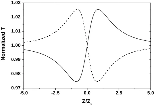
(15) 1.03. Normalized T. 1.02 1.01 1.00 0.99 0.98 0.97 -5.0. -2.5. 0.0. 2.5. 5.0. Z/Z 0 Fig. 1-4 Predicted Z-scan signal for positive (solid line) and negative (dashed line) nonlinear phase shifts.. In the preceding picture we assumed a purely refractive nonlinearity with no absorptive nonlinearities such as 2PA that will suppress the peak and enhance the valley.. If NLA and. NLR are present simultaneously, a numerical fit to the data can in principle extract both the nonlinear refractive and absorptive coefficients.. However, a second Z-scan with the aperture. removed and care taken to collect all the transmitted light can determine the NLA independently.. For 2PA alone and a Gaussian input beam, the loss nearly follows the. symmetric Lorentzian shape as a function of the sample position Z.. The magnitude of the. loss determines the NLA. This so-called open aperture Z-scan is only sensitive to NLA.. A. further division of the apertured Z-scan data (referred to as closed-aperture Z-scan) by the open-aperture Z-scan data gives a curve that for small nonlinearities is purely refractive in nature.. In this way we have separate measurements of the absorptive and refractive. nonlinearities without the need for computer fits of the Z-scans.. 1-2-5 Excite-probe Z-scan Excite-probe techniques in nonlinear optics have been employed to deduce information -7-.
(16) that is not accessible with a single-beam geometry. By using two collinear beams in a Z-scan geometry, we can measure nondegenerate nonlinearities, we can temporally resolve these nonlinearities, and we can separate the absorptive and refractive contributions. There have been several investigations that have used Z-scan in an excite-probe scheme. Z-scan can be modified to give nondegenerate nonlinearities by focusing two collinear beams of different frequencies into the material and monitoring only one of the frequencies (different polarizations can be used for degenerate frequencies). The general geometry is shown in Fig. 1-5. After propagation through the sample, the probe beam is then separated and analyzed through the far-field aperture. Due to collinear propagation of the excitation and probe beams, we are able to separate them only if they differ in wavelength or polarization.. The. former scheme, known as a two-color Z-scan, has been used to measure the nondegenerate n2 and β in semiconductors.. Fig. 1-5 Optical geometry for a two-color Z-scan.. The most significant application of excite-probe techniques in the past concerned the ultrafast dynamics of nonlinear optical phenomena.. The two-color Z-scan can separately. monitor the temporal dynamics of NLR and NLA by introducing a temporal delay in the path of one of the input beams.. These time-resolved studies can be performed in two fashions.. In one scheme, Z-scans are performed at various fixed delays between excitation and probe pulses.. In the second scheme, the sample position is fixed (e.g., at the peak or the valley -8-.
(17) position), while the transmittance of the probe is measured as the delay between the two pulses is varied. The analysis of two-color Z-scan is naturally more involved than that of a single-beam Z-scan.. The measured signal, in addition to being dependent on the parameters. discussed for the single-beam geometry, also will depend on parameters such as the excite-probe beam waist ratio, pulse-width ratio, and the possible focal separation due to chromatic aberration of the lens.. 1-3 Merits of ZnO ZnO is a kind of metal-oxide material with its melting point of around 2250 0K and self-activated crystal of hexagonal wurtzite structure with lattice constant of a=0.3249 nm and 4 c=0.5207 nm in the space group C 6v .. The deposited thin film usually belongs to. c-axis-oriented textures and was drawn much attentions because of its ultraviolet emission. The notable properties of ZnO are due to its wide band gap at room temperature and a high exciton binding energy (~60 meV) that is much higher than that of ZnSe and GaN. Furthermore, the high exciton binding energy permits excitonic recombination even at room temperature. Due to these properties, ZnO can be used as UV or blue emitting materials [20]. In addition to optical transparency throughout the visible region of the spectrum and the observed large piezo-optic and piezoelectric effects in films with c-axis oriented, trivalent cation-doped ZnO exhibits marked electrical conductivity.. The combination of these. characteristics makes ZnO a system of choice for thin film photo-electronic device applications [21].. As a candidate for ultraviolet optoelectronic device applications, the. nonlinear properties of ZnO are attractive.. 1-4 Aim of this research -9-.
(18) In this thesis we concentrate on the nonlinear response in the transparency range of semiconductors, i.e., for photon energies far enough below the band-gap energy Eg that bound-electronic nonlinearities either dominate the nonlinear response or are responsible for initiating free-carrier nonlinearities (e.g., two-photon absorption-created carrier nonlinearities). The bound-electronic nonlinearities of two-photon absorption (2PA) and the optical Kerr effect are the primary nonlinearities of interest.. In ZnO thin film, a systematic study of. second-harmonic generation as a function of the film thickness was reported [22]. Surprisingly, for very think films χ(2) as large as 18 pm/V was obtained this was larger than the value 14 pm/V for bulk single-crystal ZnO.. And in polycrystalline ZnO with c-axis. orientation a larger 2PA coefficient β (8.6 cm/GW) than that (4.2 cm/GW) of bulk single-crystal ZnO was measured with wavelength of incident laser pulse at 532 nm [23]. Besides, ZnO has large exciton bind energy and this electron-hole Coulomb interaction (effect of excitons) could lead to an enhancement of the 2PA coefficient near the two-photon resonance. Thus, a highly-qualify c-axis orientation ZnO thin film is interested to study its nonlinearities near two photon resonance with enhancement of excitons. A large two photon absorption coefficient and nonlinear refraction is observed near two photon resonance in our highly-qualify c-axis orientation ZnO thin film. A detail investigation of this ZnO thin film is worth us to study to put it in use for the field of nonlinear optical application. In Chapter 2 we briefly describe the simple two-parabolic-band second-order perturbation theory which is used to predict the dispersion of bound-electronic nonlinearity and the two-photon absorption coefficient.. In the later of Chapter 2, we describe the determination. of two photon absorption coefficient and bound-electronic nonlinearity from open-aperture Z-scan and closed-aperture one respectively. film are given in Chapter 3.. Experiments used to measure this ZnO thin. In Chapter 4 our measured values of this ZnO thin film are. compared with various theoretical models. We also compare our measured ß and n2 values with theoretical values.. At last conclusions and perspective are both given in Chapter 5. - 10 -.
(19) Chapter 2. Theoretical background. The processes of nonlinear absorption (NLA) and nonlinear refraction (NLR) in materials, in the most general case, can be considered as the interaction of two light beams having distinct frequencies (ωa and ωb) in a nonlinear medium.. In such an interaction, the two. beams can alter each other’s phase (NLR) or amplitude (NLA), the latter process requiring certain energy resonances. Note that in this type of wave mixing no new frequencies are generated. The preceding condition, known as the nondegenerate interaction, is the general case of the simple degenerate situation where the two beams have the same frequency (ωa = ωb).. Most convenient experimental arrangements, however, involve an even simpler. degenerate geometry where both beams have the same vector as well as frequency.. In this. case, which is also known as nonlinear self-action, a single beam alters its own phase and/or amplitude through propagation in a nonlinear medium. In the characterization of a nonlinear material, one determines the nonlinear change of refractive index (∆n) and change of absorption coefficient (∆a) of a material. Relations for these changes are ∆n(ωa ) = n2 (ωa ; ωa ) I a + 2n2 (ωa ; ωb ) I b. (1). ∆α (ωa ) = α 2 (ω a ; ωa ) I a + 2α 2 (ωa ; ωb ) I b. (2). and. where Ib and Ia are the irradiances of the two beams.. Here, n2 and a 2 refer to the nonlinear. refractive index and nonlinear absorption coefficients, respectively.. For photon energies hωi. satisfying E g / 2 < h(ωa + ωb ) < Eg , a 2 accounts for 2PA and is often denoted by ß.. Note that. without loss of generality, we assume that the measurement is performed on beam1, while beam 2 acts as an excitation source only. The first terms on the right-hand side of the preceding equations correspond to self-action (i.e., single-beam experiments). - 11 -. The second.
(20) terms correspond to the case of an excite-probe experiment provided that the two beams are distinguishable either by frequency and/or wavelength. The factor of 2 in front of the second term is a consequence of this distinguishability, since a higher degree of permutation is allowed in the nonlinear interaction process [5].. 2-1. Analysis of Z-scan method. 2-1-1 Bound-electronic and free-carrier nonlinearity A pair of simple equations can be used to describe the nonlinear refraction and absorption when the incident irradiance propagates within nonlinear media. d ∆φ 2π dz ′ = λ ∆n( I ) dI = −α ( I ) I dz ′. (3). where z’ is the propagation depth in the sample and α(I), in general, includes linear and nonlinear absorption terms. In the case of a cubic nonlinearity and negligible nonlinear absorption, (3) are solved to give the phase shift ∆φ at the exit surface of the sample which simply follows the radial variation the incident irradiance at a given position of the sample z. Thus,. ∆φ ( z , r , t ) = ∆φ0 ( z , t ) exp(−. 2r 2 ) w2 ( z ). (4a). with ∆φ ( z , t ) =. ∆Φ 0 (t ) 1 + z 2 / z02. (5b). ∆Φ 0 (t ) , the on-axis phase shift at the focus, is defined as ∆Φ 0 (t ) = k ∆n0 (t ) Leff. (6). whose Leff = (1 − e −α L ) / α , with L the sample length and α the linear absorption coefficient.. - 12 -.
(21) Here, ∆n0 = γ I 0 (t ) with I 0 (t ) being the on-axis irradiance at focus (i.e., z=0). By applying “Gaussian Decomposition” method, the normalized Z-scan transmittance T(z) can be calculated. The measurable quantity ∆Tp-v as the difference between the normalized peak and valley transmittance: Tp-Tv. Based on a numerical fitting, the following relation ship can be used to obtain the phase distortion on-axis.. ∆Tp − v ; 0.406(1 − S )0.268 ∆Φ 0 for ∆Φ 0 ≤ π. (7). where S = 1 − exp(−2ra2 / wa2 ) is the aperture linear transmittance, with wa denoting the beam radius at the aperture in the linear regime and ra is the aperture radius. By including nonlinear absorption, the absorption term in Eq (3) becomes α ( I ) = α + β I . With the same analysis, the transmitted power P(z,t) as follows: P( z , t ) = Pi (t )e −α L. ln[1 + q0 ( z , t )] q0 ( z , t ). (8). where q0 ( z , t ) = β I 0 Leff /(1 + z 2 / z02 ) and Pi (t ) = π w02 I 0 (t ) / 2 .. For a temporally Gaussian. pulse, (8) can be time integrated to give the normalized energy transmittance. T ( z , S = 1) =. ∞ 2 1 ⋅ ∫ ln[1 + q0 ( z , 0) e−τ ]dτ π q0 ( z , 0) −∞. (9). For q0 < 1 , this transmittance can be expressed in terms of the peak irradiance in a summation form more suitable for numerical evaluation:. [− q0 ( z, 0)]m 3/2 m = 0 ( m + 1) ∞. T ( z , S = 1) = ∑. (10). At higher irradiance level the nonlinear refraction caused by 2PA generated charge carriers, an effective fifth-order nonlinearity, becomes important.. Thus the change of refractive index. will become: (∆n) ; γ I 0 + Cσ r I 02. (11). where C = 0.23( β t0 / hω ) for low linear absorption (α0L< 0.2), t0 is the pulse width.. - 13 -.
(22) 2-2 Coefficients of nonlinear absorption and refraction The on-axis (r=0) Z-scan transmittance for a cubic nonlinearity and a small phase change ( ∆Φ = 1 ) can be derived. The far-field condition d >> z0 can be used to further simplify the equation to give a geometry-independent normalized transmittance as T ( z , ∆Φ) ; 1 +. 4x ∆Φ 0 ( x2 + 9)( x2 + 1). (12). where x=z/z0. The normalized transmittance of closed-aperture Z-scan is expressed as [29] T ( z ) = 1 + T∆Φ ( z ) + T∆Ψ ( z ). (13). By consider the on-axis Z-scan, and Gaussian beam in the low-irradiance limit, the two nonlinear terms can be expressed as, T∆Φ =. 4x ∆Φ 0 ( x2 + 9)( x2 + 1). T∆Ψ = −. 2( x 2 + 3) ∆Ψ 0 ( x2 + 9)( x2 + 1). (14) (15). where x=z/z0. By fitting closed-aperture Z-scan trace with Eq. (13), it is unambiguous to determine ß and ? with ∆Ψ 0 = β I 0 Leff / 2. (16). ∆Φ 0 = kγ I 0 Leff. (17). and. where I0 is the on-axis irradiance of the laser beam at focus, k is the wavevector and Leff=(1-e-aL)/a, a is the linear absorption coefficient and L is the thickness of sample.. 2-3. Dispersion of bound-electronic nonlinearities: Two-Band. Model - 14 -.
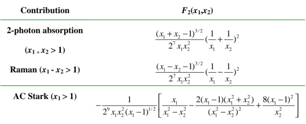
(23) By using a two-parabolic-band (TPB) model with A ·p perturbation to calculate the bound-electronic nonlinear susceptibilities [25][26] including 2-photon absorption (2PA), the AC Stark effect, and Raman contributions.. It shows a strong systematic dispersion in the. bound-electronic nonlinearity (electronic Kerr effect n2) near the two-photon-absorption edge. With the two-photon-absorption spectrum predicted by TPB, we can predict the observed universal dispersion, scaling and values of n2.. 2-3-1 Nonlinear absorption The resulting representation of a 2 for 2PA has the simple form α 2 (ω1 , ω2 ) = K. Ep n01n02 Eg 3. F2 ( x1 , x2 ). (18). where K is a material-independent constant: K=. 29 π 1 5 (4πε 0 ) 2. e4. (19). m0c 2. The function F2 involves only the parameters x1=hω1/Eg and x2= hω2/Eg and reflects the band structure and intermediate states.. In TPB model, F2 contains contributions from 2PA,. Raman, and optical Stark effects. These different components are listed in Table I [27].. Contribution. F2(x1,x2). 2-photon absorption. ( x1 + x2 − 1)3 / 2 1 1 2 ( + ) 27 x1 x22 x1 x2. (x1 + x2 > 1). ( x1 − x2 − 1)3 / 2 1 1 2 ( − ) 27 x1 x22 x1 x2. Raman (x1 - x2 > 1) AC Stark (x1 > 1). −. x1 1 2( x1 − 1)( x12 + x22 ) 8( x1 − 1) 2 − + 29 x1 x22 ( x1 − 1)1/ 2 x12 − x22 ( x12 − x22 ) 2 x22 . Table I Contributions to the nonlinear absorption spectral function F2(x1,x2). - 15 -.
(24) From Table I the 2PA contribution to the nonlinear absorption for x1 = x2 = x is F2 =. (2 x − 1)3 / 2 25 x5. (20). Now experimental data ß (ße) for can be plotted by calculating the experimental value of the function F2, F2e, as given below. The absolute magnitude for this function is then a fitting parameter K: F2e (hω / Eg ) =. 1 n02 Eg3 β e K Ep. (21). Measurements of degenerate of on a number of II-VI and III-V semiconductors fit this model using K = 3100 cm GW-1 eV5/2 in units where Ep and Eg are in electronvolts (3.2 × 10-55 mks). This compares favorably with the theoretical value of K = 1940 cm GW-1 eV5/2 (1.99 × 10-55 mks) give by Eq. (15).. This is because the theory underestimates the empirical value. because only one valence band (ligh-hole) has been considered, and the contribution of the heavy-hole band has been ignored.. 2-3-2 Nonlinear refraction With the nondegenerate nonlinear absorption coefficient a2 (ω1; ω2) determined, the next step is to perform the KK transformation to obtain the n2 coefficient. The result of this calculation is n2 (ω1 , ω2 ) = K ′. Ep n01n02 Eg 4. G2 ( x1 , x2 ). (22). where the dispersion function G2 is given by G2 ( x1; x2 ) =. 2 ∞ F2 (x ′; x2 ) dx′ π ∫0 x′2 − x12. (23). and. - 16 -.
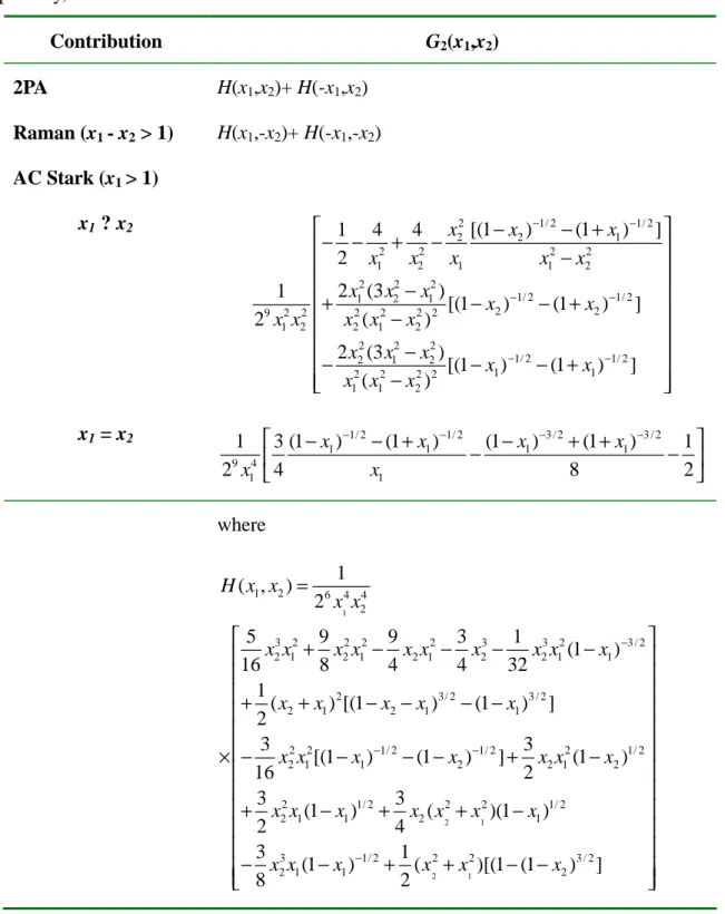
(25) K′ =. hcK 24 he 4 = 2 5π ε 0 2 m0 c. (24). Using the function F2 given in Table I, the integration in Eq. (23) can be performed analytically. After the long-wavelength divergent terms for each contribution are removed separately, the final results are set out in Table II. Contribution. G2(x1,x2). 2PA. H(x1,x2)+ H(-x1,x2). Raman (x1 - x2 > 1). H(x1,-x2)+ H(-x1,-x2). AC Stark (x1 > 1) x1 ? x2. x1 = x2. 1 4 4 x22 [(1 − x2 ) −1/ 2 − (1 + x1 ) −1/ 2 ] − − 2 + 2 − x12 − x22 2 x1 x2 x1 1 2 x12 (3 x22 − x12 ) −1/ 2 −1/ 2 + [(1 − ) − (1 + ) ] x x 2 2 29 x12 x22 x22 ( x12 − x22 ) 2 2 x 2 (3 x2 − x2 ) − 22 2 1 2 22 [(1 − x1 ) −1/ 2 − (1 + x1 ) −1/ 2 ] x1 ( x1 − x2 ) . 1 9 4 2 x1. 3 (1 − x1 ) −1/ 2 − (1 + x1 ) −1/ 2 (1 − x1 ) −3 / 2 + (1 + x1 ) −3 / 2 1 − − 8 2 x1 4. where. H ( x1 , x2 ) =. 1 2 x14 x24 6. 3 3 1 3 2 5 3 2 9 2 2 9 2 −3 / 2 16 x2 x1 + 8 x2 x1 − 4 x2 x1 − 4 x2 − 32 x2 x1 (1 − x1 ) + 1 ( x + x ) 2 [(1 − x − x )3/ 2 − (1 − x )3 / 2 ] 2 1 1 2 2 1 3 3 × − x22 x12 [(1 − x1 ) −1/ 2 − (1 − x2 ) −1/ 2 ] + x2 x12 (1 − x2 )1/ 2 2 16 3 2 3 + x2 x1 (1 − x1 )1/ 2 + x2 ( x 22 + x12 )(1 − x1 )1/ 2 4 2 3 3 1 −1/ 2 2 2 3/2 − x2 x1 (1 − x1 ) + ( x 2 + x1 )[(1 − (1 − x2 ) ] 8 2 Table II The nondegenerate dispersion function for the electronic Kerr component of n2, calculated by a KK - 17 -.
(26) transformation of F2 (Table 1). The dispersion (G2) of n2 as predicted by Eq. (23) along with data (n2e) from several experiments scaled with G ( x) = e 2. n02 Eg4 K ′ Ep. n2e. (25). The prefactor K', as given by Eq. (25) is 3.2 × 10-81 (mks units). If we use the K as determined by a best fit to the 2PA experiment data, we find K' ˜ 5 × 10-81 (mks units).. This. compares well with K' ˜ 9 × 10-81 (mks units) determined by an overall best fit to the experimental values of n2 in semiconductors [26]. As in the 2PA case, it is more convenient to define the K' factor in mixed units such that n2 is given by square centimeters per watt and Ep and Eg are given in electronvolts.. In this K' ˜ 6 × 10-11 (cm2/W)(eV)7/2 corresponds to the. overall best fit to semiconductor n2 data. As pointed out or the 2PA case, the factor of 2 to 3 discrepancy between theory and experiments can be attributed in par to using a single valence band (light hole) and ignoring the transition originating from the heavy-hole valence band. Moreover, as described by Sheik-Bahae et al. [28], inclusion of electron-hole Coulomb interaction by multiplying the F2 function by a generalized exciton enhancement factor will further improve the agreement between theory and experiment.. - 18 -.
(27) Chapter 3. 3-1. Experiments. XRD analysis of ZnO thin film growth by Laser MBE. The ZnO thin film was grown on fused silica by Laser MBE deposition with 2hr sputtering at 600 ℃ and in-situ annealed for 1hr at 700 ℃. The crystal structures of the ZnO thin films were inspected by a JPN MAC Science MXP18 X-ray diffractometer offered by NTHU using a Cu Ka X-ray as exciting source (λ=1.5405 ). The operating voltage and current of the system is 20kV and 5mA, respectively and the scanning step and rate is 0.020 and 4 degree/min.. 3-2 Photoluminescence and transmission spectra A UV He-Cd laser (Kimmon IK5552R-F) operating at the 325 nm is utilized as pumping source for Photoluminescence (PL). Fig. 3-1 shows the block diagram of PL detection system, it includes the reflective mirror, focusing and collecting lenses, and the single-grating monochromators (TRIAX 320) with a photo-multiplier tube (PMT-HVPS) which is equipped with a photon counter for detection. The TRAIX 320 monochromator has three selective gratings among 600, 1200 and 1800 grooves/mm. 800 KV.. We used standard fluorescent lamps to calibrate our spectral response of. spectrometer and detector. of 0.1 nm.. The normal applied voltage of PMT is. The signals of PL spectra are exposed about 0.1 sec at each step. The 0.1nm-resolution can be resolved with this monochromator while the. entrance and exit slits are both opened about 50 µm.. Fig. 3-1 Sketch diagram of photoluminescence spectra. - 19 -.
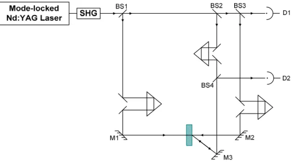
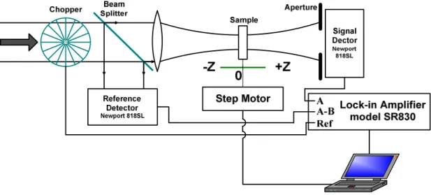
(28) We use the HP-8453 UV-VIS spectrometer for the transmission spectra measurement. The scan range of the wavelength is from 200 to 900 nm and increment is 1nm. The incident light was perpendicular to the sample and the transmitted light was detected by this transmission spectra.. 3-3 Single beam Z-scan apparatus The apparatus of single beam Z-scan is shown in Fig. 3-2.. A tunable Kerr-lens. mode-locked Ti:sapphire laser between 740 and 850 nm wavelength with a repetition rate of 93.3 MHz is used as the exciting source.. The spatial transverse mode distribution of the. laser is nearly Gaussian and the pulse width at the half maximum is around 100-fs.. The. incident light is chopped by a chopper with 1.33 KHz frequency and divided by a beam splitter into two beams. light.. The reflected beam was detected by the photodiode as the reference. The transmitted beam, as the exciting light, was focused by a 50 mm focal-length lens. and the beam radius ω0 of focused is around 17-18 µm at the focus point.. Our sample was. mounted on a step motor and moved along the z direction with 1.25 µm movement per step. A finite aperture was placed in the far field to control the transmittance of the light in the z-scan measurement.. The signal are simultaneously detected by two photodiodes and sent to. a lock-in amplifier (Model: SR830) to increase the signal-to noise ratio.. After the open. aperture (S=1) was scanned, an aperture was placed in front of the signal detector to trace the close aperture (S=0.4) scan.. To purely obtain the nonlinear refraction, a simple division of. the closed aperture scan by open-aperture scan will be performed. The divided Z-scan curves exhibit the expected features, namely, a valley-peak (v-p) for the positive nonlinearity and a peak-valley (p-v) for the negative one. An irradiance-dependent Z-scan study will be performed to investigate the nonlinear refraction caused by two photon absorption (2PA) generated charge carriers, an effective fifth-order nonlinearity.. - 20 -.
(29) Fig. 3-2 The Z-scan apparatus with reference detector and lock-in amplifier to minimize background and maximize the signal-to-noise ratio respectively.. - 21 -.
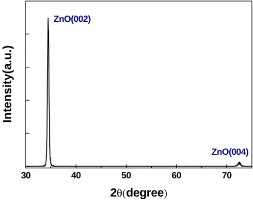
(30) Chapter 4. 4-1. Results and Discussion. XRD. The thickness of ZnO film was measured about 1 µm by surface profile offered by Nano Facility Center (NFC) at NCTU.. Result of X-ray diffraction measurement is shown in Fig.. 4-1. By comparing with JCPDS#36-145 and our diffraction pattern in Fig. 4-1, strong diffraction lines were observed only from the (002) and (004) planes.. This result indicates. that the ZnO sample growth is highly-qualify single crystal thin film with the crystallographic c-axis being parallel to the growth direction (perpendicular the surface of this sample).. Intensity(a.u.). ZnO(002). ZnO(004). 30. 40. 50. 60. 2θ(degree) Fig. 4-1 Result of X-ray diffraction measurement. - 22 -. 70.
(31) 4-2. Photoluminescence Spectra. With using the PL spectra shows in 3-2, the near-band edge emission and band-gap of this ZnO thin film can be investigated. ZnO film is around 381 nm.. As Fig. 4-2 shows, the near band edge emission of this. This emission is the near-band edge emission of ZnO in most. epitaxial method. The broad band emission of 450-550 nm is contributed from the substrate of fused silica and deep level of ZnO.. This is due to lattice mismatch of fused silica and. ZnO. This can be solved to replace the substrate of fused silica by double-side polished sapphire.. But this kind of sapphire substrate can contribute the nonlinear absorption and. refraction when the wavelength of incident pulse is near two-photon resonance of ZnO thin film.. It will lead some errors in calculation of nonlinear absorption and refraction of ZnO. thin film. Moreover, this contribution of deep level of ZnO is tenfold smaller than the near-band edge emission; this will not induce a large amount of nonlinearities in Z-scan measurements and misunderstanding of this ZnO thin film.. The sapphire, hence, may not. the proper candidate of substrate for the ZnO thin film in our Z-scan measurement.. Intensity(a.u.). 381. Quartz & deep level. 350. 400. 450. 500. 550. 600. 650. Wavelength(nm) Fig. 4-2 Result of Photoluminescence spectra measurement - 23 -. 700.
(32) 4-3. Transmission Spectra. A simple formula 4-1(Ref R. Swanepoel .pdf) can be used for the calculation of sample thickness via transmission spectra for our measurement. d=. λ1λ2 2(n2 λ1 − n1λ2 ). (26). where n1 and n2 are the refractive indices at two adjacent maxima (or minima) at λ1 and λ2. By applying λ1 =642 nm, λ2 =759 nm and n1 =1.98, n2=1.96, we can evaluate sample thickness d is about 1023 nm which is close to the result of surface profile measurement. 100 90. Transmittance(%). 80 70 60 50 40 30 20 10 0 300. 400. 500. 600. 700. 800. 900. Wavelength(nm) Fig. 4-3 Result of transmission spectra measurement. 4-4 Measurement of Z-scan A Z-scan with a fully open aperture (S=1) is in sensitive to nonlinear refraction (thin sample approximation).. Such Z-scan traces with no aperture are expected to be symmetric. with respect to the focus (z=0) where has a minimum transmittance (e.g., multiphoton absorption) or maximum transmittance (e.g., saturation of absorption).. Thus, the. coefficients of nonlinear absorption can be easily calculated from such transmittance curves. - 24 -.
(33) The low-irradiance (I0=0.54GW/cm2) open aperture and closed aperture Z-scan traces of single crystal ZnO thin film with c-axis orientation thin film at 748 nm-wavelength are shown in Fig. 4-4. (a) and (b) respectively.. Figure 4-4(a) shows normalized open-aperture Z-scan. transmittance of ZnO (filled squares) and the best fitting curve (solid line).. The significant. decrease in the normalized transmittance was observed as the sample approached to the focus (Z=0).. Figure 4-4(b) shows normalized closed-aperture (S=0.4) Z-scan transmittance (filled. squares) and the best fitting curve (solid line).. As seen in Fig. 4-4(a), the change in. transmittance for the measurement without an aperture is symmetric with respect to the focus. The observations imply that two-photon absorption can be occurred at 748nm-wavelength of input laser beam. As seen in Fig. 4-4(b), the asymmetric curve is observed and it implies a nonlinear refractive phenomenon takes place.. A prefocal transmittance minimum (valley). followed by a postfocal transmittance maximum (peak) is the Z-scan signature of a positive refractive nonlinearity.. Therefore, it reveals this ZnO thin film is a positive nonlinear. refractive medium when the wavelength of input laser beam is around 748 nm. To remove nonlinear absorption from closed-aperture data and obtain the purely nonlinear refraction, the closed-aperture measurement is divided by the open-aperture one at the same irradiance. The division of the intensity-dependent Z-scans results (Fig. 4-4(b)/(a)) is shown in Fig. 4-5(a) where the filled squares are the experimental result and the solid lines are the theoretical fitting result. The valley-peak configuration is clearer than Fig. 4-4(b) showed symmetric result. By fitting the division data, the phase distortion can be obtained.. And the nonlinear. index can be deduced from this phase distortion at this irradiance. The theoretical fit is obtained by setting β= 1440 cm/GW in fig. 4-4(a) and γ = 2.8 × 10⁻¹¹ cm2/W (1.323 × 10⁻¹¹ esu) in fig. 4-4(b) with the peak irradiance 0.538 GW/cm2 at the focus within sample.. - 25 -.
(34) Normalized Transmittance. 1.01. (a). 1.00. 0.99. 0.98. 0.97. (b). Normalized Transmittance. 1.02 1.01 1.00 0.99 0.98 0.97 0.96 -10. -5. 0. 5. 10. 15. Z(mm) Fig. 4-4 (a) Open-aperture Z-scan trace (filled squares) of ZnO measured with a pulse intensity of 0.54 GW/cm2 at 748 nm. The solid line is a fitting curve. (b) Closed aperture (S=0.4) Z-scan trace (filled squares) and fitting curve (solid line). The data in (a) and (b) were fitted with β= 1440 cm/GW and γ = 2.8 × 10⁻¹¹ cm2/W.. A series of divided Z-scan results versus peak laser irradiance as measured on the same ZnO thin film is shown in Fig. 4-5 (The filled squares are experimental data and solid curve - 26 -.
(35) are theoretical fitting curve).. The ? Tp-v (difference between the normalized peak and valley. transmittance: Tp-Tv) can be derived directly from the divided results and the phase distortion with various laser irradiances can be obtained easily from these fitting curves. of. refractive. ∆Φ =. index. can. be. obtained. from. these. phase. The change. distortion. with. 2π 1 − exp(−α L) ∆n , where ? is the wavelength of incident laser, a is the absorption λ α. coefficient and L is the thickness of sample. A plot of ß and ? n versus peak laser irradiance as measured from various Z-scan on the same ZnO thin film is shown in Fig. 4-6 and 4-7, respectively. The average TPA coefficient, β, is obtained from Fig. 4-6 as 1905 cm/GW with an uncertainty of 15% arising predominantly from the irradiance calibration.. This. irradiance-dependent Z-scan study of the ZnO thin film indicates that for irradiance I0 < 0.76 GW/cm2, the nonlinear refraction is dominated by a third-order effect.. This is depicted in. Fig. 4-7 where the measured nonlinear index change ? n varies linearly with the irradiance. The adjusting γ is obtained from Fig. 4-7 as 2.63 × 10⁻¹¹ cm2/W (n2 = 1.245× 10⁻¹¹ esu). Theoretically, the nonlinear refraction at low irradiance levels is dominated by a third-order effect and this nonlinearity was attributed to n2, the nonlinear refraction caused by bound electrons (electronic Kerr effect).. At higher irradiance levels, however, the nonlinear. refraction caused by the two photon absorption generated free charge carriers, an effective fifth-order nonlinearity, becomes significant. This is indicated in Fig. 4-7 by the deviation of above I0 =0.76 GW/cm2 from the line representing the cubic nonlinearity.. - 27 -.
(36) Normalized Transmittance. 2. 2. 1.06. (d) I0=0.81GW/cm. (a) I0=0.54GW/cm. 1.04 1.02 1.00 0.98 0.96 0.94 2. Normalized Transmittance. 1.06. 2. (b) I0=0.65GW/cm. (e) I0=0.91GW/cm. 2. (f) I0=0.97GW/cm. 1.04 1.02 1.00 0.98 0.96 0.94. Normalized Transmittance. 1.06. 2. (c) I0=0.75GW/cm. 1.04 1.02 1.00 0.98 0.96 0.94 -10. -5. 0. 5. 10. 15. Z(mm). -10. -5. 0. 5. 10. 15. Z(mm). Fig. 4-5 The closed aperture trace divided by the open aperture trace with different pulse intensity, the filled squares are experimental data and the solid lines are fitting curves. (a) 0.54 GW/cm2, (b)0.65 GW/cm2, (c) 0.75 GW/cm2, (d)0.81 GW/cm2, (e)0.91 GW/cm2 and (f)0.97 GW/cm2.. - 28 -.
(37) 4. Experimental data guide for eye. β × 103(cm/GW). 3. 2. 1. 0 0.4. 0.5. 0.6. 0.7. 0.8. 0.9. 1.0. 1.1. 1.2. 2. I0(GW/cm ) Fig. 4-6 Measured TPA coefficients (filled blocks) plotted as a function of I0. The horizontal solid line is a guide for the eye and yields β = 1905 cm/GW.. 3.5. 2. ∆n=γI0+Cσr I0. 3.0. -2. ∆n(×10 ). 2.5 2.0. ∆n=γI0. 1.5 1.0 0.5 0.0 0.0. 0.2. 0.4. 0.6. 0.8. 1.0. 1.2. 2. I0(GW/cm ) Fig. 4-7 ∆n directly derived from ∆Tp-v plotted as a function of I0 for ZnO. The slope of the straight-line best fit to the data yields γ = 2.63 × 10⁻¹¹ cm2/W. The line represents a cubic (n2 type) nonlinearity.. The deviation from. the line is indicative of higher order refractive effects arising from two-photon generated charge carriers. - 29 -.
(38) To clearly estimate the free carrier nonlinearity, a simple procedure [30] is present. This procedure is performed at various irradiances, and the results of these fitted ? n are divided by I0.. If there were no higher-order nonlinearities, this procedure would give a horizontal line. with vertical intercept γ in the plot of ? n/I0 versus I0.. Thus, with free-carrier refraction, the. curve of a plot of ? n/I0 versus I0 is a straight line with an intercept γ of and a slope of Cσr. where C is given by C ; 0.23( β t0 / hω ) for low linear absorption (α0L < 0.2). t0 is the pulse width of incident laser. A relation is given below ∆n ; γ I 0 + Cσ r I 02. (27). By applying this method to this ZnO thim film, a plot of ? n versus I0 is shown in Fig. 4-7. Fig. 4-7 shows the low-irradiance results (I0 < 0.76 GW/cm2), the third-order nonlinear refraction is attributed to bound-electronic effects and γ = 2.63 × 10⁻¹¹ cm2/W is obtained from the vertical intercept of this horizontal line. The higher-irradiance results for I0 > 0.76 GW/cm2 is shown in Fig. 4-7.. The bound-electronic nonlinearity γ = 2.21 × 10⁻¹¹ cm2/W (n2. = 1.155 × 10⁻⁸ esu) is obtained from the nonzero-intercept of the fitted parabolic line and the refractive-index change per carrier-pair density σr = 4.51 × 10⁻²⁰ cm3 is obtained from this parabolic line. This relation also can be derived as: ∆n / I 0 ; γ + Cσ r I 0. (28). A plot of ? n/I0 versus I0 is shown in Fig. 4-8.. The bound-electronic nonlinearity γ = 2.21 ×. 10-11 cm2/W (n2 = 1.155 × 10⁻⁸ esu) is obtained from the nonzero-intercept of the fitted straight line and the refractive-index change per carrier-pair density σr = 4.51 × 10⁻²⁰ cm3 is obtained from the slope of this straight line.. The bound-electronic nonlinearity derived from. straight and parabolic line is close, this deviation is mainly from the inaccuracy of experiment. The data (open squares) in Fig. 4-8 is the TPA coefficients versus incident irradiance and the dashed line is a guide for the eye. - 30 -.
(39) 6 3.2 5 4. -2. 2. 2.8 3. 2.6 2.4. 2. 2.2. 1. 2.0 0.0. β × 103(GW/cm2). ∆n/I0×10 (cm /GW). 3.0. 0 0.2. 0.4. 0.6. 0.8. 1.0. 2. I0(GW/cm ) Fig. 4-8 Measured TPA coefficients (open squares) versus irradiance and ∆n/I0 (filled squares) plotted as a function of I0 for the ZnO thin film. 1905 cm/GW.. The horizontal dashed line is a guide for eye with vertical intercept β =. The intercept of linear best fit to the data gives γ = 2.21 × 10⁻¹¹ cm2/W, and the slope yields σr =. 4.51 × 10⁻²⁰ cm3.. The measured TPA coefficient, bound-electronic and free-carrier nonlinearity are larger than those with 25-ps laser pulse, frequency-doubled, mode-locked, Q-switched Nd-YAG laser [31].. Excitonic enhanced in optical nonlinearity is dominated when the incident laser. light is near two-photon resonance. Thus, a wavelength-dependent Z-scan is performed to investigate this excitonic enhancement of ZnO near two-photon resonance. TPA coefficient versus wavelength of incident laser is shown in Fig 4-9.. The dashed line is. half of exciton bind energy subtract from half of energy of band-gap of ZnO. of arrow is two-photon resonance energy.. The measured. The position. When the wavelength of incident laser light is far. away two-photon resonance, the measured TPA coefficient is smaller.. As wavelength of. incident laser light is below this dashed line, the measured TPA coefficient is drastically - 31 -.
(40) decreased.. It likes a resonance behavior at this dashed line.. enhancement near two-photon resonance. [32].. This is clearly due to excitonic. This behavior could also be observed in ZnTe. In GaN thin film, TPA coefficient is 18 times larger than theoretical value is. observed[33] which is mainly from the excitonic enhancement.. There are 12 meV of. exciton binding energy in ZnTe and 27 meV one in GaN and 60meV in ZnO. The thermal energy is about 26 meV.. At room temperature, the exciton is still exist in ZnO.. Due to this. large exciton binding energy 60 meV in ZnO, the TPA is drastically enhanced near two-photon resonance.. Compared with 25-ps measured TPA coefficient of ZnO single. crystal [31], it is about 400 times enhancement when the wavelength of incident laser light is 748 nm.. 2200. (Eg-Eb)/2. 2000 1800 1600. β(cm/GW). 1400 1200 1000 800 600 400. Eg/2. 200 0 740. 745. 750. 755. 760. 765. 770. 775. 780. 785. λ(nm) Fig. 4-9 Measured TPA coefficients (filled squares) versus wavelength λ(nm) for the ZnO thin film.. When the. wavelength of incident laser is larger than the half energy of exciton-to-valance band, the TPA coefficients is smaller. It also reveals an excitonic enhancement near two-photon resonance.. - 32 -.
(41) The measured bound-electronic nonlinearity at two-photon resonance is also larger than theoretical value [26]. The measured nonlinear refractive index versus wavelength is shown is Fig. 4-10.. When the wavelength of incident laser light is far from two-photon resonance,. the nonlinear refractive index is smaller.. It reveals a two-photon resonance behavior in this. ZnO thin film. This fitted K’ in Fig. 4-11 is 2000 times larger than theoretical value. This behavior could also be obtained in GaN thin film [34].. Because of a smaller exciton bind. energy 27 meV than one of ZnO, this enhancement is not remarkable in GaN thin film. By DFWM, a very large third-order optical nonlinearity in ZnO microcrystalline thin film is observed [35].. It is due to absorption strength for excitation near the exciton and the. band-to-band transitions.. From this, the excitonic enhancement is dominated near. two-photon resonance in ZnO thin film. 2.2. (Eg-Eb)/2. 1.0. 2.0. 0.8. -8. 1.6. n2 × 10 (esu). -11. 2. n2 × 10 (cm /GW). 0.9 1.8. 0.7. 1.4 1.2. 0.6. Eg/2. 0.5. 1.0 740. 745. 750. 755. 760. 765. 770. 775. 780. 785. λ(nm) Fig. 4-12 Measured nonlinear refractive index (filled squares) versus wavelength λ(nm) for the ZnO thin film. When the wavelength of incident laser is larger than the half energy of exciton-to-valance band, nonlinear refractive index is smaller. It reveals an excitonic enhancement near two-photon resonance.. - 33 -.
(42) Dispersion Function G2. 0.10. Theoretical Experimental Data. 0.05. 0.00. -0.05. -0.10 0.0. 0.2. 0.4. 0.6. 0.8. 1.0. ? ω /Eg Fig. 4-11 Measured nonlinear refractive index (open squares) versus h? /Eg for the ZnO thin film.. The solid. line is the theoretical value with K’is 2000 times larger than theoretical value.. 25. 15. -20. 3. σr × 10 (cm ). 20. 10. 5. Eg/2 0 740. 745. (Eg-Eb)/2 750. 755. 760. 765. 770. 775. 780. 785. λ(nm) Fig. 4-12 Measured free-carrier nonlinearity (filled squares) versus wavelength λ(nm) for the ZnO thin film. When the wavelength of incident laser is near the half energy of exciton-to-valance band, the free-carrier nonlinearity is larger.. It reveals an excitonic enhancement. - 34 -.
(43) The free-carrier nonlinearity versus wavelength of incident laser light is shown in Fig. 4-12. When the wavelength of incident laser light is near half energy of exciton-to-valance band, the free-carrier nonlinearity is larger.. This is also an excitonic enhance behavior.. I0(GW/cm2). ?F. Z0(mm). ? n/I0. 1. 0.54. 0.114. 1.205. 0.0260. 2. 0.59. 0.129. 1.570. 0.0269. 3. 0.64. 0.137. 1.311. 0.0264. 4. 0.70. 0.142. 1.14. 0.0260. 5. 0.75. 0.156. 1.250. 0.0262. 6. 0.80. 0.176. 1.356. 0.0279. 7. 0.86. 0.189. 1.330. 0.0281. 8. 0.91. 0.206. 1.386. 0.0294. 9. 0.97. 0.226. 1.353. 0.0304. 10. 1.02. 0.223. 1.397. 0.0285. 11. 1.07. 0.24. 1.430. 0.0293. Average. 1.334 Table III The fitting results of division of Z-scan.. - 35 -.
(44) Chapter 5. 5-1. Conclusions and perspectives. Conclusions. Optical nonlinearities (including two-photon absorption coefficient, bound-electronic and free-carrier nonlinearities) of ZnO thin film growth by Laser-MBE is first observation near two-photon resonance.. This ZnO thin film is inspected by XRD which indicated this film. is a highly c-axis orientation quality and the result of PL reveals a strong free-exciton luminescence at room temperature.. The measured result of visible light’s range of. transmission spectrum reveals it has a high transparency of visible light’s range.. Because. of this high c-axis orientation quality, the biggest two-photon absorption coefficient that we measured at 748nm-wavelegth of incident laser light is ≈1905 cm/GW. This strong two-photon absorption is about 400 times larger than that of ZnO bulk measured at 532 nm with 25-ps pulse-width.. The two-photon absorption coefficient is disappeared above. 780nm-wavelength of incident laser light source. Moreover, there is a drastic downgrade near 762nm which is equal the half of band-edge energy plus exciton bind energy. resonance behavior of excitonic enhancement near two-photon resonance.. It is a. The measured. biggest bound-electronic nonlinearity of ZnO thin film that we measured is at 748nm-wavelength of incident laser light. It’s about 2000 times larger than theoretical value. From the wavelength-dependent Z-scan, the energy of incident laser light is smaller than half band-gap energy, the measured bound-electronic nonlinearity become smaller. The biggest bound-electronic nonlinearity of ZnO thin film ranging from 748-780 nm that we measured is about 2000 times larger than theoretical value. Compared with the results of DFWM of ZnO microcrystalline thin film, that measured third-order optical nonlinearity is about 100 times larger than us.. This discrepancy of result of DFWM and Z-scan is due. to the absorption strength of near excitonic resonance, band-to-band transition and different - 36 -.
(45) wavelength of incident laser light source.. Thus 2000 times larger than theoretical value of. bound-electronic nonlinearity is due to two-photon resonance with excitonic enhancement. The free-carrier nonlinearity of ZnO thin film at 748 nm is about 40 times larger than that of ZnO bulk measured at 532 nm with 25-ps pulse-width. near two-photon resonance.. Its two-photon absorption strength. The wavelength-dependent Z-scan reveals the resonance. behavior near (Eg-Eb)/2.. 5-2. Perspectives. Free-excitons dominate near band-edge emission at room temperature and bound-excitons will dominate at low temperature.. It’s a very important issue to understand the nonlinearities. of bound-excitonic enhancements at low temperature.. A temperature-dependent Z-scan is. needed to improve. At higher temperature, the free-exciton binding energy will be covered by thermal energy. At this point, the nonlinearities of ZnO thin film will decay if those are dominated by free-excitons.. This temperature-dependent Z-scan will provide additional. evidence that excitons enhanced and dominated optical nonlinearities near two-photon resonance at low temperature and room temperature. Besides, a tunable light source with more wide range is needed to measure these nonlinearities of ZnO thin film without two-photon resonance.. A second-harmonic-generation of Ti:Sapphire laser is also needed to. study these nonlinearities of ZnO thin film with near excitonic resonance and compare with the results of DWFM of a 55-µm thickness ZnO microcrystalline thin film. Theoretically, dispersion of bound-electronic nonlinearity of ZnO thin fill will be observed near excitonic resonance.. In other words, the bound-electronic nonlinearity of ZnO thin film with UV light. pumping will be negative.. Moreover, the influence of thickness to third-order optical. nonlinearity are the same with second-order one.. Furthermore, the effect of Fabry-Perot. interferometer is significant with a normal incident to surface of sample. To find out the carrier dephasing time of ZnO by time-resolved Z-scan is essentially needed. - 37 -. With.
(46) time-resolved two-color Z-scan, nondegenerate optical nonlinearities will be study.. These. techniques will facilitate us to comprehensive study the origins of optical nonlinearities of ZnO thin film which is a highly c-axis orientation quality.. - 38 -.
(47) Reference [1]. Braunstein, R. and Ockman, N. “Optical Double-photon Absorption in CdS,” Phys. Rev. 134, A499-A507. 1964.. [2]. Haug, H. Optical Nonlinearities and Instabilities in Semiconductors. Academic Press. 1988.. [3]. Miller, A. and Duncan, D. “Optical Nonlinearities in Narrow Gap Semiconductors.” In Optical Properties of Narrow-Gap Low-Dimensional Structures, (C. M. Sotomayer Torres, J. C. Portal, J. C. Mann, and R. A. Stradling, eds), Plenum, New York, 1987.. [4] Adair, R., Chase, L. L., and Payne, S. A. “Nonlinear Refractive Index of Optical Crystals,” Phys. Rev. B 39, 3337-3350. 1989. [5]. Boyd, R. W.. Nonlinear Optics. Academic Press, San Diego, 1992.. [6]. Agrawal, G. P. Nonlinear Fiber Optics, Academic Press, 1989.. [7]. Spence, D. E., Kean, P. N., and Sibbett, W. “60-fsec Pulse Generation From a Self-Mode-Locked Ti-Sapphire Laser,” Opt. Lett. 19, 4. 1991.. [8]. Gibbs, H. M. Optical Bistability: Controlling Loght with Light, Academic Press. 1985.. [9]. Mizrahi, V., Delong, K. W., Stegeman, G. I., Saifi, M. A., and Andrejeco, M. J., “Two-Photon Absorption as a Limit to All-Optical Switching,” Opt. Lett. 14, 1140-1142, 1989.. [10] A. A. Armstrong, N. Bloembergen, J. Ducuing, and P. S. Pershan, “Interactions between light waves in a nonlinear dielectric,” Phys. Rev., vol. 127, pp. 1918-1939, 1962. [11] R. De Salve, D. J. Hagan, M. Sheik-Bahae, G. Stegeman, and E. W. Van Stryland, “Self-focusing and self-defocusing by cascaded second-order effects in KTP,” Opt. Lett., vol. 17, pp. 28-30, 1992. [12] G. Assanto, G. Stegeman, M. Sheik-Bahae, and E. Van Stryland, “All-optical switching devices based on large nonlinear phase shifts from second harmonic generation,” Appl. Phys. Lett., vol. 62, pp. 1323-1326, 1993. [13] W. E. Torruellas, Z. Wang, D. J. Hagan, E. W. Van Stryland, G. I. Stegeman, L. Torner, C. R. Menyuk, “Observation of Two-Dimensional Spatial Solitary Waves in a Quadratic Medium,” Phys. Rev. Lett., vol. 74, pp. 5036-5039, 1995. [14] M. Zavelani-Rossi, G. Cerullo, and V. Magni, “Mode Locking by Cascading of Second-Order Nonlinearities,” IEEE J. Quantum Electron., vol. 34, no. 1, pp. 61-70, 1998. [15] Sheik-Bahae, M. Said, A. A., Wei, T. H., Hagan, D. J., and Van Stryland, E. W., “Sensitive Measurements of Optical Nonlinearities Using a Single Beam,” IEEE J. Quantum Electron. QE-26, 760-769, 1990. [16] Xia, T., Hagan, D. J., Sheik-Bahae, M. and Van Stryland, E. W., “Eclipsing Z-Scan Measurement of ?/104 Wavefront Distortion,” Opt. Lett. 19, 317-139. 1994. [17] Wang, J., Sheik-Bahae, M., Said, A. A., Hagan, D. J., and Van Stryland, E. W., “Time-Resolved Z-Scan Measurements of Optical Nonlinearities,” J. Opt. Soc. Am. B11, 1009-1017, 1994,. [18] Fisher, R. A. Optical Phase Conjugation. Academic Press, 1983 [19] Sheik-Bahae, M. Said, A. A., and Van Stryland, E. W., “Sensitivity, Single Beam n2 Measurements,” Opt. Lett. 14, 955-957. [20] Bixia Lin and Zhuxi Fu, Yunbo Jia, “Green Luminescent Center in Undoped Zinc Oxide Films Deposited on - 39 -.
(48) Silicon Substrates,” Appl. Phys. Lett. 79, 943, 2001. [21] Gregory J. Exarhos, Shiv K. Sharma, “Influence of Processing Variables On The Structure and Properties of ZnO Films,” Thin Solis Film 270, 27-32. 1995. [22] Gang Wang, G. T. Kiehne, G. K. L. Wong, J. B. Ketterson, X. Liu and R. P. H. Chang, “Large second harmonic response in ZnO thin films” Appl. Phys. Lett. 80, 401-403, 2002. [23] Nakazawa M, Watanabe Y, Tsuchiya T and Fujitsu S, “Measurement of two-photon absorption coefficient of transparent polycrystalline zinc oxide with c-axis orientation,” J. Ceram. Soc. Jpn.” 104, 918-921, 1996. [24] Van Vechten, J. A. and Aspnes, D. E., “Franz-Keldysh Contribution to Third-Order Optical Susceptibilities,” Phys. Lett. A 30, 346, 1969. [25] Sheik-Bahae M., D.J. Hagan and E. W. Van Stryland, “Dispersion and Band-Gap Scaling of the Electronic Kerr Effect in Solids Associated with Two-Photon Absorption,” Phys. Rev. Lett. 65, 96-99, 1990 [26] Sheik-Bahae M., Hutchings, D. C., Hagan, D. J., and Van Stryland, E. W., “Dispersion of Bound-Electronic Nonlinear Refraction in Solids,” IEEE J. Quantum Electron. QE-27, 1296-1309, 1991. [27] Sheik-Bahae M. and Van Stryland, E. W., “Optical Nonlinearities in Bulk Semiconductors,” Semiconductors and Semimetals, 58, 257-318, 1999. [28] Sheik-Bahae M., J. Wang, and Van Stryland, E. W., “Nondegenerate Optical Kerr Effect in Semiconductors,” IEEE J. Quantum Electron., QE-30, 249-255, 1994. [29] M. Yin, H. P. Li, S. H. Tang and W. Ji, “Determination of nonlinear absorption and refraction by single Z-scan method,” Applied Physcs B, 70, 587-591, 2000. [30] A. A. Said, M. Sheik-Bahae, D. J. Hagan, T. H. Wei, J. Young, and E. W. Van Stryland, “Determination of bound-electronic and free-carrier nonlinearities in ZnSe, GaAs, CdTe and ZnTe,” J. Opt. Soc. Am. B, 9, 405-414, 1992. [31] X. J. Zhang, W. Ji, and S. H. Tang, “Determination of optical nonlinearities and carrier lifetime in ZnO,” J. Opt. Soc. Am. B, 14, 1951-1955, 1997. [32] C. C. Lee and H. Y. Fan, “Two-photon absorption with exciton effect for degenerate valence band,” Phys. Rev. B, 9, 3502-3516, 1974 [33] Chi-Kung Sun, et. al., “Two-photon absorption study of GaN,” Appl. Phys. Lett. 76, 439-441, 2000. [34] Yong-Liang Huang, et. al., “Femtosecond Z-scan measurement of GaN,” Appl. Phys. Lett. 75, 3524-3526, 1999. [35] Weili Zhang, el. Al., “Third-order optical nonlinearity in ZnO microcrystallite thin films,” Appl. Phys. Lett. 75, 3521-3523, 1999.. - 40 -.
(49)
數據
+7

相關文件
We do it by reducing the first order system to a vectorial Schr¨ odinger type equation containing conductivity coefficient in matrix potential coefficient as in [3], [13] and use
在1980年代,非晶矽是唯一商業化的薄膜型太 陽能電池材料。非晶矽的優點在於對於可見光
Xianggang zaji (miscellaneous notes on Hong Kong) was written by an English and translated into Chinese by a local Chinese literati.. Doubts can therefore be cast as to whether
S15 Expectation value of the total spin-squared operator h ˆ S 2 i for the ground state of cationic n-PP as a function of the chain length, calculated using KS-DFT with various
“Polysilicon Thin Film Transistors Fabricated at 100℃ on a Flexible Plastic Substrate,” IEEE Electron Device Meeting, p. “Polysilicon Thin Film Transistors
Sugii, “Junction profile engineering with a novel multiple laser spike annealing scheme for 45-nm node high performance and low leakage CMOS technology,” in IEDM
This project is the optical electro-mechanic integration design and manufacturing research of high magnifications miniaturized size zoom lens and novel active high accuracy laser
Keywords:Micro-array Biological Probes, E-Beam Evaporator, Active RFID, Laser Annealing, Bioelectric Impedance, Thin Film Transistor
