Single mode 1.27-
µ
m InGaAs:Sb-GaAs-GaAsP Quantum Well
Vertical Cavity Surface Emitting Lasers
Hao-Chung Kuo, Yi-An Chang, Ya-Hsien Chang, Jung-Tang Chu, Min-Ying Tsai, and
Shing-Chung Wang
Department of Photonics and Institute of Electro-optical Engineering, National Chiao-Tung
University, Hsinchu, Taiwan, R. O. C,
Keywords: Strain-compensated, High-speed electronics, VCSELs, InGaAsP/InGaP, proton-implant
ABSTRATE
1.27 µm InGaAs:Sb-GaAs-GaAsP vertical cavity surface emitting lasers (VCSELs) were grown by metalorganic chemical vapor deposition (MOCVD) and exhibited excellent performance and temperature stability. The threshold current changes from 1.8 to 1.1 mA and the slope efficiency falls less than ~35% as the temperature raised from room temperature to 70oC. With a bias current of only 5mA, the 3dB modulation frequency response was measured to be 8.36 GHz, which is appropriate for 10 Gb/s operation. The maximal bandwidth is measured to be 10.7 GHz with modulation current efficiency factor (MCEF) of ~ 5.25 GHz/(mA)1/2. These VCSELs also demonstrate high-speed modulation up to 10 Gb/s from 25oC to 70oC.
1. INTRODUCTION
Long-wavelength vertical cavity surface-emitting lasers (VCSELs) are key devices in optical fiber metropolitan-area networks (MAN). The most promising results regarding low-cost long-wavelength lasers or VCSELs, have been obtained using GaInAsN quantum wells (QWs) grown on GaAs substrates [1-5]. The large conduction band offset improves the temperature performance over that of conventional InP-based materials. The GaAs system provides high-performance AlGaAs/GaAs DBR mirrors and permits the use of the well-established oxide-confined GaAs-based VCSEL manufacturing infrastructure. However, GaInAsN is a very challenging material system from a growth perspective: (1) incorporating N into the InGaAs QW is difficult and increases the non-radiative (monomolecular and Auger) recombination, reducing the material gain and increasing the transparency carrier density [6]; (2) during post– growth annealing, the nitrogen diffuses out from the quantum well and blue-shifts the optical emission. Recently, Koyama et al. [7] and Tansu et al. [8] employed of highly strained InGaAs QW active lasers to extend the emission wavelength 1.2 µm. Highly strained InGaAs VCSELs with a photoluminescence (PL) peak at 1.205 µm and a laser emission wavelength of ~1.26-1.27 µm have demonstrated very promising performance and continuous–wave (CW) operation at up to 120oC as well as 10 Gb/s operation.[9]. However, the emission wavelength of 1.26 µm barely meets optical communication standards, such as IEEE 820.3ae 10Gb/s Ethernet. Furthermore, this laser performs relatively poorly at room temperature due to the large negative gain-cavity offset. Antimony (Sb) present during GaInAsN growth has been believed to act as a surfactant and improve PL [10]. The authors have observed that adding Sb into samples with high In content sharply increases the PL intensity, and have found that the alloy thus formed not only behaves as a surfactant but contributes significantly to red-shift of the optical emission [10]. Additionally, adding a surfactant such as Sb [11] and Te [12] significantly increases the critical layer thickness of InGaAs on GaAs. This work presents high-performance InGaAs:Sb-GaAs-GaAsP QWs VCSELs grown by metal organic chemical vapor deposition (MOCVD). The LIV performance and high speed performance proved these VCSELs a good candidate of long wavelength VCSEL
All structures were grown on semi-insulating GaAs (100) substrates by low pressure metal organic chemical vapor deposition (MOCVD). The group-V precursors were the hydride sources AsH3 and PH3. The trimethyl alkyls of
gallium (Ga), aluminum (Al), indium (In) and Antimony (Sb) were the group-III precursors. The epitaxial structure was as follows (from bottom to top) - n+-GaAs buffer, 40.5-pair n+-Al0.9Ga0.1As/n+-GaAs (Si-doped) distributed Bragg
reflector (DBR), undoped active region, p-Al0.98Ga0.02As oxidation layer, 25-pair p+-Al0.9Ga0.1As/p+-GaAs DBR
(carbon-doped) and p+-GaAs (carbon-doped) contact layer. The graded-index separate confinement heterostructure (GRINSCH) active region consisted mainly of a double QWs active region In0.41Ga0.59As:Sb-GaAs-GaAs0.85P0.15
(60Å/100Å/100Å), with PL emission at 1.214 µm, embedded between two linear-graded AlxGa1-xAs (x = 0 to 0.6 and
x = 0.6 to 0) confinement layers (growth temperature = 550°C with AsH3/TMSbflow ratio ~50). The thickness of the
cavity active region was 1λ. Carbon was used as the p-type dopant in the DBR to increase the carrier concentration (2-3×1018 cm-3). The interfaces of both the p-type and n-type Al0.9Ga0.1As/GaAs DBR layers are linearly graded to reduce
the series resistance. The optical characteristics of QWs were optimized through PL measurement and structural analysis. The details of growth optimization will be published elsewhere [13].
Fig. 1 compares the photoluminescence spectra of InxGa1-xAs QW with various In contents (x = 0.41 and 0.42),
and that of In0.41Ga0.59As QW with incorporated Sb. All samples have a well thickness of 60Å with a GaAs spacer and a
GaAs0.85P0.15 strain-compensating layer. The PL peak emission wavelengths (λp) of the grown
In0.41Ga0.59As/GaAs/GaAsP and In0.41Ga0.59As:Sb/GaAs/GaAsP QWs are 1.194 and 1.214 µm, respectively. A red-shift
of 20 nm is observed. The full-width at half maximum (FWHM) of the PL emission peak from In0.41Ga0.59As:Sb is
larger and the PL intensity slightly lower. The red-shift of InGaAs:Sb can be attributed to the Sb in the alloy constituent and red-shifts the optical emission. As the Indium composition increases to 0.42, the FWHM of the PL emission increases significantly and the PL intensity drops dramatically. These changes can be explained by the dislocations and the formation of non-radiative defects of the 60Å In0.42Ga0..58As/GaAs/GaAsP QW where 60Å exceeds the critical layer
thickness. From the reflectivity spectrum of an as-grown VCSEL structure, the cavity mode is centered at 1.266 µm. The large stop band of over 90nm results from the large index contrast of AlGaAs/GaAs DBRs. The cavity mode and the gain mode offset is determined to be 52nm.
Fig. 2 schematically depicts the VCSEL structure. A processing sequence involved six photomasks to fabricate oxide-confined polyimide-bridged VCSELs with coplanar wave-guide probe pads. This process was designed to minimize capacitance while keeping a reasonably low resistance [14]. Device fabrication began with the formation of cylindrical mesas with a diameter of 30 µm by etching the surrounding semiconductor into the bottom n-type mirror to a depth of 5 µm, using an ICP-RIE system. The sample was wet-oxidized in a 420 oC steam environment for 20 min to form the current aperture and provide lateral index guiding to the lasing mode. The oxidation rate was 0.6 µm/ min for the Al0.98Ga0.02As layer, so the oxide extended 12.5 µm from the mesa sidewall. Ti/Au was evaporated to form the
p-type contact ring, and AuGeNiAu was evaporated onto the etched n–buffer layer to form the n-p-type contact, which is connected to the semi-insulating substrate. Contacts were alloyed for 30 sec at 420 oC using RTA. After the contact
1050 1100 1150 1200 1250 1300 1350 1400 0.0 0.2 0.4 0.6 0.8 In0.41Ga0.59As-GaAsP QW In 0.41Ga0.59As:Sb-GaAsP QW In 0.42Ga0.58As-GaAsP QW L u m in es ce n c e I n te n si ty ( a.u .) Wavelength (nm)
Fig. 1 Comparison of the photoluminescence spectra of InGaAs with different In composition and In0.41Ga0.59As with Sb incorporation.
formation, the photosensitive polyimide was spun on the sample to form insulation. Ti–Au was deposited to a thickness of from 200 to 3000 Å to form the metal interconnects and coplanar waveguide probe pads. Heat treatment following metal deposition was applied to strengthen the metal-to-polyimide adhesion. Finally, surface relief etching with a diameter of 3.5 µm was performed to a depth of ~λ/2 for single-mode operation [15].
3. RESULTS
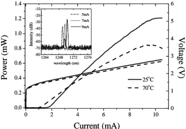
The DC characteristics of completed VCSELs were measured using a probe station, an Agilent 4145A semiconductor parameter analyzer and an InGaAs photodiode. The spectra of the InGaAs:Sb-GaAs-GaAsP VCSELs were measured using an Advantest Q8381A optical spectrum analyzer. Fig. 3 plots curves of temperature-dependent light output and voltage versus current (LIV). The devices exhibit single transverse mode characteristics at a lasing wavelength of ~1.27 µm, with a side mode suppression ratio (SMSR) of >30dB as in the inset in Fig. 3 over the whole operating range. In addition, the wavelength shifted with dissipated power at a rate of 0.105 nm/mW. Given a wavelength shift with temperature of 0.074 nm/K obtained from large-area pulsed VCSELs (not published), a thermal impedance was calculated to be 1.42 K/mW. Notably, the maximal single mode output power exceeds 1.2mW at room temperature (0.8mW at 70°C). Output power rollover occurs as the current increases above 10mA at 25°C (9.5mA at 70°C). The threshold current changes between 1.8 and 1.1 mA with temperatures from 25°C to 70°C and the slope efficiency drops less than ~35 % from 0.17 to 0.11 mW/mA due to the large gain-cavity offset. The resistance of the
N-contact P-Contact SI-GaAs substrate Polyimide bridge N-GaAs buffer layer oxidation Si3N4 P-pad Surface relief N-contact P-Contact SI-GaAs substrate Polyimide bridge N-GaAs buffer layer oxidation Si3N4 P-pad Surface relief
Fig. 2 Schematic cross section of high speed VCSEL structure. The oxide-confined aperture is 5 µm and the surface relief size is 3.5 µm.
Fig. 3 Temperature-dependent light output and voltage versus current (LIV) curves. Inset is the emission spectra of InGaAs:Sb-GaAs-GaAsP VCSELs at different driving currents.
0 2 4 6 8 10 0.0 0.2 0.4 0.6 0.8 1.0 1.2 1.4
Current (mA)
Po
w
er (m
W
)
0 1 2 3 4 5 6V
o
ltage (
V
)
25oC 70oC 1264 1268 1272 1276 -80 -70 -60 -50 -40 -30 -20 -10 5mA 7mA 9mA In te n sity ( d B ) wavelength (nm) 0 2 4 6 8 10 0.0 0.2 0.4 0.6 0.8 1.0 1.2 1.4Current (mA)
Po
w
er (m
W
)
0 1 2 3 4 5 6V
o
ltage (
V
)
25oC 70oC 1264 1268 1272 1276 -80 -70 -60 -50 -40 -30 -20 -10 5mA 7mA 9mA In te n sity ( d B ) wavelength (nm)VCSEL is ~120 Ω and the capacitance is ~0.1 pF. Accordingly, parasitic effects limit the devices to a frequency response of around 13 GHz.
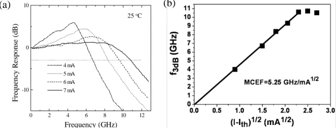
The small signal response of VCSELs as a function of bias current was measured at 25oC using a calibrated vector network analyzer (Agilent 8720ES) with wafer probing and a 50 µm multimode optical fiber connected to a New Focus 25 GHz photodetector. Fig. 4(a) indicates the modulation frequency increases with the bias current, until it flattens at a bias of about 7mA. At a bias current of only 5mA, the maximum 3dB modulation frequency response is measured as 8.36 GHz, which is suitable for 10 Gb/s operation. In Fig. 4(b), the 3dB bandwidth (f3dB) is plotted as a
function of the bias current. At low bias currents, the bandwidth increase in proportion to the square root of the current as expected from the rate equation analysis. The saturation of bandwidth was clearly observed as bias current increases above 7mA which might be attributed to heating effect or spatial hole burning. The maximal bandwidth is measured to be 10.7 GHz with modulation current efficiency factor (MCEF) of ~ 5.25 GHz/(mA)1/2 and the differential gain at room temperature was estimated to ~ 2×10-16 cm2.
To measure the high-speed VCSEL under large signal modulation, microwave and light wave probes were used in conjunction with a 10 Gb/s pattern generator (MP1763 Anritsu) with a pseudorandom bit sequence of 223-1 and a 12.5 GHz photoreceiver. Eye diagrams were obtained for back-to-back (BTB) transmission on VCSEL. Fig. 5(a) demonstrates that the room temperature eye diagram of the presented VCSEL biased at 6 mA, with data up to 10 Gb/s
(a)
(b)
Fig. 5(a) Room temperature (b) 70°C eye diagram of our VCSEL data up to 10 Gb/s and 6dB extinction ratio. The time scale is 15 ps/div and the vertical scale is 90 mV/div for (a) and 60 mV/div for (b).
(b)
25 oC 0 2 4 6 8 10 12 -10 0 10 4 mA 5 mA 6 mA 7 mA F re q u enc y R e sp on se (d B ) Frequency (GHz)(a)
Fig. 4 (a) Small signal modulation measurement on VCSELs, the maximal bandwidth is measured to be 10.7 GHz with MCEF is ~ 5.25 GHz/(mA)1/2. (b) 3-dB bandwidth (f3dB) is plotted as a function of the bias
and an extinction ratio of 6dB. The clear open eye pattern indicates good performance of these InGaAs:Sb VCSELs with the rise time Tr of 30 ps, the fall time Tf of 41 ps, and jitter(p-p) < 20 ps. The VCSELs also exhibit superior
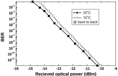
performance at high temperature. The reasonably open eye-diagram in Fig. 5(b) demonstrates the high-speed performance of the VCSEL (biased at 7mA) at 10Gb/s with an extinction ratio of 6dB at 70°C. One can notice that more rising edge jitter appeared at 70°C than room temperature. This is not surprising, since the differential gain and output optical power both reduced at high temperature which directly increased the turn-on jitter and overshoot effect. In general, maintaining a high extinction ratio in high temperature generally means sacrificing jitter performance and overshoot performance [16]. To further investigate the high speed performance, bit-error rate (BER) analysis was performed. Fig. 6 shows average received power dependence of the bit error rate at 10Gbps modulation under back to back transmission and temperature of 25°C and 70°C. In this experiment, multimode fiber was aligned to realize the highest coupling efficiency. An error rate of 10-12 was achieved without any indication of a BER floor. This result further verifies the superior performance of the presented VCSELs.
4. CONCLUSION
High-performance InGaAs:Sb-GaAs-GaAsP QWs VCSELs with an emission wavelength of 1.27 µm were successfully demonstrated. The VCSELs exhibit a very low threshold current, good temperature performance, and a high modulation bandwidth of ~ 10.7 GHz with MCEF of ~5.25 GHz/(mA)1/2. The VCSELs also demonstrate high-speed modulation up to 10 Gb/s from 25oC to 70oC. The results reveal the performance of the InGaAs:Sb VCSELs comparable to that of GaInAsN VCSELs, but with better thermal stability. Longer wavelength is possible with incorporating more Sb or In content into the quantum well by reducing of growth temperature. Thus, the InGaAs:Sb VCSEL should be viable low cost light source of optical fiber data link systems.
REFERENCE
1. T. Takeuchi, Y.-L. Chang, M. Leary, A. Tandon, H.-C. Luan, D. Bour, S. Corzine, R. Twist, M. Tan, “1.3 µm InGaAsN vertical cavity surface emitting lasers grown by MOCVD”, Electron. Lett., vol. 38, pp.1438 – 1440, 2002. 2. M. Kondow, T. Kitatani, S. Nakatsuka, M.C. Larson, K. Nakahara, Y. Yazawa, M. Okai, and K. Uomi, “GaInNAs:
a novel material for long-wavelength semiconductor lasers ”, IEEE J. Select. Topic Quantum Electron., vol. 3, pp. 719–730, 1997.
3. K. D. Choquette, J.F. Klem, A.J. Fischer, O. Blum, A.A. Allerman, I.J. Fritz, S.R. Kurtz, W.G.Breiland, R. Sieg, K.M. Geib, J.W. Scott, and R.L. Naone, “ Room temperature continuous wave InGaAsN quantum well vertical-cavity lasers emitting at 1.3 µm”, Electron. Lett., vol. 36, no. 16, pp. 1388–1390, 2000.
Fig. 6 (a) 25°C and (b) 70°C average received power dependence of the bit error rate at 10 Gbps modulation under back to back transmission.
-16 -15 -14 -13 -12 -11 -10 -9 10-11 10-10 10-9 10-8 10-7 10-6 10-5 10-4 10-3 10-2 25oC 70oC @ back to back BE R
4. Nobuhiko Nishiyama, Masakazu Arai, Satoshi Shinada, Munechika Azuchi, Tomoyuki Miyamoto, Fumio Koyama, and Kenichi Iga,“Highly strained GaInAs–GaAs Quantum-Well Vertical-Cavity Surface-Emitting Laser on GaAs (311)B substrate for stable polarization operation”, IEEE J. Select. Topic Quantum Electron., vol. 7, pp.242–248, 2001.
5. M. Kawaguchi, T. Miyamoto, E. Gouardes, D. Schlenker, T.Kondo, F. Koyama and K. Iga “Lasing Characteristics of Low-Threshold GaInNAs Lasers Grown by Metalorganic Chemical Vapor Deposition”, Jpn. J. Appl.Phys., vol. 40, pp. L744–L746, 2001.
6. N. Tansu and L. J. Mawst, “Temperature sensitivity of 1300-nm InGaAsN quantum-well lasers”,IEEE Photon.
Technol. Lett., vol. 14, pp.1052–1054, 2002.
7. F. Koyama, D. Schlenker, T. Miyamoto, Z. Chen, A. Matsutani, T. Sakaguchi, and K. Iga, “1.2 highly m strained GaInAs/GaAs quantum well lasers for single mode fiber datalink,” Electron. Lett., vol. 35, no. 13, pp.1079–1081, 1999.
8. N. Tansu, J. Y. Yeh, and L. J. Mawst, “Extremely-Low Threshold-Current-Density InGaAs Quantum Well Lasers with Emission Wavelength of 1215-1233 nm,” Appl. Phys. Lett., vol.82(23), pp. 4038-4040, 2003.
9. P. Sundgren, R.M. von Wurtemberg, J. Berggren, M. Hammar, M. Ghisoni, V. Oscarsson, E. Odling, and J. Malmquist, “High-performance 1.3 µm InGaAs vertical cavity surface emitting lasers”, Electron. Lett., vol. 39, pp. 1128 – 1129, 2003.
10. V. Gambin, Ha Wonill, M. Wistey, Yuen Homan, S.R. Bank, S.M. Kim, and J.S. Harris, “GaInNAsSb for 1.3-1.6 µm-long wavelength lasers grown by molecular beam epitaxy”, IEEE J. Select. Topic Quantum Electron., vol. 8, pp. 795 – 800, 2002.
11. J. C. Harmand, L. H. Li, G. Patriarche, and L. Travers, “GaInAs/GaAs quantum-well growth assisted by Sb surfactant: Toward 1.3 mm emission”, Appl. Phys. Lett., vol 84, pp. 3981- 3983, 2004.
12. J. Massies, N. Grandjean, and V. H. Etgens, “Surfactant mediated epitaxial growth of InxGal-xAs on GaAs (00I)”,
Appl. Phys. Lett. vol. 61, pp. 99- 101, 1992.
13. H.C. Kuo, Y.S. Chang, H. H. Yao and S. C. Wang to be presented in ICMOVPE XII conference, 2004 14. H.C. Kuo, Y.S. Chang, F.Y. Lai, T.H. Hsueh, L.H. Laih, and S.C. Wang,“High-speed modulation of 850 nm
InGaAsP/InGaP strain-compensated VCSELs. “Electron. Lett., vol. 39, pp. 1051 – 1053, 2003.
15. Heiko J. Unold, Safwat WZ Mahmoud, Roland Jäger, Martin Grabherr, Rainer Michalzik, and Karl Joachim Ebeling, “Large-Area Single-Mode VCSELs and the Self-Aligned Surface Relief “, IEEE J. Select. Topics
Quantum Electron., vol. 7, pp. 386-392, 2000.
16. T. Aggerstam, R. M. V. Wütemberg, C. Runnström, E. Choumas, “Large aperture 850 nm oxide-confined VCSELs for 10Gb/s data communication”, Photonics West, San Jose, CA, p.p 19 Proc. SPIE Vol. 4649 (2002)