Johnson Lee*, 1, Harold N. Spector**, 2, and Wu Ching Chou3
1 Department of Physics, Chung Yuan Christian University, Chung-Li, Taiwan 32023, R.O.C. 2 Department of Physics, Illinois Institute of Technology, Chicago, Illinois, 60616, USA
3 Department of Electrophysics, National Chiao Tung University, Hsin-Chu, Taiwan 30010, R.O.C.
Received 28 January 2005, revised 12 July 2005, accepted 20 July 2005 Published online 6 September 2005
PACS 73.21.La, 73.63.Kv, 78.67.Hc
We have performed a self-consistent calculation for the energy band profiles and energy levels of cubic quantum dots, solving both the Schrödinger and Poisson’s equations. In particular, we examined the effect of doping on these levels both in the presence and absence of a positive test charge. We found that the number of levels the cubic dot supported depended on the size of the dot, and that the energy of the levels decreased in the presence of a positive test charge. Moreover, we found that the energy levels of both the singlet and triplet states in the dot increased with the doping density. The quasi-Fermi level was found to be lower in the presence of a positive test charge than in its absence, and the quasi-Fermi level increased sharply with increasing doping density both in the absence and presence of the test charge. With very high doping the Fermi level is located in the barrier while with low doping the Fermi level is located down be-low the ground state energy which implies that the probability of finding an electron in a dot is very small. We also find that at high doping levels the lowest energy states are no longer confined in the dot. The po-tential energy profile was found to be dramatically affected by both the doping and the presence of a posi-tive test charge. The profile was found to become asymmetric when the test charge was displaced from the center of the dot.
© 2005 WILEY-VCH Verlag GmbH & Co. KGaA, Weinheim
1
Introduction
In recent years, tremendous efforts have been put into the development of quantum dot (QD) semicon-ductor nanostructures. QDs are considered to be the limit of electronic confinement and have been widely studied because they provide ideal structures to replace conventional quantum well lasers [1]. These quantum nanostructures can be either microfabricated from a quantum well structure modified by lithographic and etching techniques to achieve lateral confinement [2 – 4] or grown using the high strain epitaxy technique called the Stranski – Krastanov (S – K) growth method [5, 6]. The semiconductor QDs formed in the S – K phase transition are called self-organized or self-assembled dots and are the subject of intensive study [7, 8]. Depending on the crystal growth method and conditions, structures of different shapes have been grown and reported. Usually, the material of the QDs possesses a smaller energy gap with a larger lattice constant than the matrix material, which possesses a larger energy gap with a smaller lattice constant. To avoid oxidation, QDs are capped with the matrix material. Recently, GaN QDs in an AlN matrix were successfully grown on Si(111) by molecular beam epitaxy (MBE). Stacking of QD planes with properly chosen dot sizes was demonstrated to emit white light [9]. Furthermore,
electro-* Corresponding author: e-mail: [email protected] ** e-mail: [email protected]
phys. stat. sol. (b) 242, No. 14 (2005) / www.pss-b.com 2847
Paper
optical characterization of CdSe QD laser diodes has been reported [10], and the life time of these de-vices has so far been limited to about 400 hours in continuous wave operation [11].
It is well known that since semiconductor lasers are often heavily doped and operate at high injected carrier densities, it is necessary to consider the effects of these high doping densities on the density of states, the energy band profiles, and the binding energies. At high impurity concentrations, the free carri-ers serve to screen the Coulomb potential energy of the ionized impurities and reduce the ionization energies. Depending on the doping profiles of the semiconductors, electron – electron interactions can cause band bendings and deform the energy band profiles. In the case of the QD lasers, since most elec-trons and holes are confined inside the dots, the doping densities also affect energy sub-levels. Accurate energy-band profiles (or diagrams) are important in designing devices with unique electronic and optical properties. The more accurate the energy-band profiles can be plotted, the better the desired properties of the devices can be understood, because these energy band profiles involve self-consistent solutions of a set of transport equations [12 – 14]. Among the transport equations for the devices, the Poisson equation describes the electrostatic potential with the non-uniform charge distributions in conjunction with the quasi-Fermi level, while the Schrödinger equation describes the quantum-size-effects of the confinement potential profile together with the electrostatic potential energy.
The theoretical calculations of the basic properties of the two-dimensional electron or hole systems in quantum wells have been well developed. However, the geometry of QDs with additional degrees of quantum confinement (due to the finite potential barriers) imposes boundary conditions that complicate the problems in solving the Schrödinger equation. In the case of the one-particle Schrödinger equation, if the shape of the QDs is spherical, the solutions can be obtained analytically [15]; otherwise, numerical methods [15 – 17] must be applied. When the valence band mixing and the spatial variation of the confin-ing potentials due to strain are significant, the confinement energy levels must be evaluated by usconfin-ing those more sophisticated models [18 – 21] such as an 8 × 8 Hamiltonian from the eight-band k ⋅ p theory. When QDs are doped with high impurity concentrations and the band bendings due to the space charges occur, the Schrödinger equation and the Poisson equation due to the space charge must be self- consis-tently solved to determine the energy band profiles and energy levels.
The main purpose of this paper is to investigate the influences of the doping impurity concentrations on the band edges, the confinement energy levels, the quasi-Fermi level and the Coulomb potential en-ergy of an ionized impurity inside or outside of a QD. A self-consistent calculation of the Poisson equa-tion and the one-particle Schrödinger equaequa-tion for a cubic QD with a finite potential barrier was pro-posed. Since we adopted the one-particle Schrödinger equation to determine the confinement energy levels, we limit our discussions on the band bending to the conduction band edges only. In this paper, we do not take into account the strain effects due to the lattice mismatch. In Section 2, we formulate an itera-tive numerical scheme to solve the Schrödinger equation and the Poisson equation until a self-consistent solution with a desired accuracy is reached. Section 3 presents the results of our numerical calculations for GaAs/GaAlAs cubic QDs. Finally, a summary is presented in Section 4.
2 Self-consistent calculation for energy band profiles
and energy levels of cubic QDs
Consider a larger cubic box with dimensions Lx = Ly = Lz = L of a barrier material that surrounds a smaller cubic QD with dimensions a = b = c of a well material where Lx and a are along the x-axis, Ly and b are along the y-axis and Lz and c are along the z-axis. We call this large box a super-cell. Assume that L
is much larger than c and the centers of both cubes are located at (0, 0, 0). We consider that a sample contains Ncell super-cells and is uniformly n-doped with an impurity concentration ND.Assume that all the impurities are singly ionized. On the average, there are Ni = NDL3 ionized donors and Ni electrons in a super-cell. Here Ni is correlated with the Fermi statistics. The electrostatic potential energy Vp(x, y, z) due to the space charge in a super-cell is determined by the Poisson equation. Suppose that in a super-cell a particle with an effective mass m*(x, y, z) is confined by a finite confinement potential Vc(x, y, z). If the particle is inside the QD (well) region, we assign m* = mw and Vc = 0; otherwise we assign m* = mb,
me
mass approximation with a total potential energy of (Vc+Vp) which is defined as the potential profile Vpp becomes dimensionless and is given by:
e c p [ ] , *( , , ) m V V E m x y z Ψ Ψ Ψ Ê ˆ - —ÁË ◊ —˜¯ + + = (1) p D ( , , )x y z V 8π [N n x y z( , , ) χδ(x xi) δ(y yi) δ(z zi)] κ + —◊ — = - + - - - (2) and 2 k f 1 B | | ( , , ) 2 , ( ) 1 exp J k k n x y z E E k T Ψ = = -È + Ê ˆ ˘ Á ˜ Í Ë ¯˙ Î ˚
Â
(3)where Ek and Ψk are the kth eigen-energy of E and eigen-function of Ψ, respectively, and J = J
d + Jc is the
total number of possible eigenstates where Jd is the number of discrete levels in a QD and Jc is the num-ber of quasi-continuum levels in the matrix; κ is the dielectric constant of the QD; kB is the Boltzmann constant; Ef is the quasi-Fermi level for the conduction electrons; (xi, yi, zi) is the ionized impurity loca-tion and χ equals 1 (0) to include (exclude) a test point charge. Equation (1) is the Schrödinger equation and ensures that the Hamiltonian operator is Hermitian and the current probability density is continuous even for a space-dependent effective mass m*(x, y, z) at the interface of the heterojunction. Equation (2) is the Poisson equation, and the space charge consists of the fully ionized impurity concentration ND, free carrier density n, and a point test charge. Equation (3) gives the Fermi statistics which describe the dis-tribution of the Ni ionized electrons in a super-cell as mentioned earlier.
The numerical method for solving the Schrödinger equation (Eq. (1)) is well-known [15 – 17] and we discuss it briefly here. The envelope function of a QD, Ψ(x, y, z), is expanded in terms of a set of or-thogonal periodic functions (OPF), ψlmn(x, y, z), where the quantum numbers l, m and n are positive inte-gers. We have , , ( , , ) lmn lmn( , , ) l m n r z A r z Ψ φ =
Â
ψ φ (4)and the OPF, ψlmn(x, y, z), are given by
2 1 2 1 2 1
( , , ) sin lπ sin π sin π .
2 2 2
lmn x y z x m y n z
L L L L L L
ψ = ÊË - ˆ¯ ÊË - ˆ¯ ÊË - ˆ¯ (5)
Substituting expression (5) into Eq. (1), multiplying the left side by ψ*l′m′n′, and finally integrating over the volume L3 of the super-cell yields the matrix equation
( lmnl m n nn mm ll) lmn 0 ,
lmn M -Eδ δ δ A =
Â
′ ′ ′ ′ ′ ′ (6)where the matrix elements are given by [15 – 17]
e c p * * d d d ( ) . * x y z lmnl m n l m n lmn l m n lmn L L L m M x y z V V m ψ ψ ψ ψ È ˘ = Í — ◊— + + ˙ Î ˚
ÚÚÚ
′ ′ ′ ′ ′ ′ ′ ′ ′ (7)phys. stat. sol. (b) 242, No. 14 (2005) / www.pss-b.com 2849
Paper
Equation (6) is solved numerically for the eigen-energies and eigen-functions. The Poisson equation is solved by using the finite difference method. Because the matrix obtained from the Poisson equation is a real band symmetric matrix, we use the band storage mode to save the computer’s memories. To corre-late ND and Ef, we invoke the charge neutrality of the entire system without the test charge (χ = 0) by substituting Eq. (3) into Eq. (2) and integrating both sides of Eq. (2) over the volume of the super-cell. We have 3 D i f 1 B 2 , ( ) 1 exp J k k N L N E E k T + = = = -+
Â
(8)where the fact that the wave function Ψk is normalized is used. Equation (8) indicates that the total num-ber of ionized impurities must equal to the total numnum-ber of electrons which reside in a QD and in the matrix of the super-cell. Recall that total number of energy levels J in Eq. (8) is a sum of Jd discrete energy levels in the QD plus Jc quasi-continuum levels in the matrix. If Ni is larger than 2Jd, Ef must be located in the barrier to accommodate Ni– 2Jd electrons while if Ni is much less than 1, i.e., the probabil-ity of finding an electron in a super-cell is small, Ef must be located down below the ground state energy level. It is important to note that when Eq. (8) is used to calculate Ef, dimensions (Lx, Ly, Lz) of the super-cell must be chosen so large that the wavefunction Ψk and energy Ek approach to their asymptotic values and are independent of Lx, Ly and Lz.
In order to do the self-consistent calculation, in the first iteration, we simultaneously solve Eq. (6) together with Eqs. (2) – (3) and (8) by setting Vp = 0 because we know nothing about Vp yet. However, when the first iteration is done, Vp is determined from the Poisson equation. In the 2nd iteration, V
p
ob-tained from the first iteration is then put into Eqs. (6) and (7) which are solved together with Eqs. (2) – (3) and (8). These procedures are iterated several times until a self-consistent solution with the desired accu-racy is reached.
3 Numerical results and discussion
Self-consistent calculation for GaAs/Ga0.63Al0.37As cubic QDs (Lx = Ly = Lz = L) has been performed by using the following parameters: (inside the QD) Vc = 0, m = 0.0665 mw* e, κw = 13.1; (in the matrix)
4 5 6 7 8 9 10 40 80 120 160 200 240 280 ND=1014/cm3 E3triplet J d=3 E2triplet Jd=2 E1singlet Jd=1 Ej (m e V ) c (nm)
Fig. 1 First three energy levels in a quantum dot are shown as a function of the dot size c in the absence (χ = 0, hollow circles) and presence (χ = 1, solid circles) of a test charge at xi = yi = zi = 0 when the dop-ing density is low (ND = 1 × 1014 cm3).
4 6 8 10 -80 -60 -40 -20 0 HD=1014/cm3 Ef (m e V ) c (nm)
Fig. 2 Quasi-Fermi level is shown as a function of the dot size c with ND = 1 × 10¹⁴ /cm3 in the absence (χ = 0, hollow circles) and presence (χ = 1, solid circles) of a test charge at xi = yi = zi = 0.
Vc = V0 = 276 meV, m = 0.0858 m*b e, κb = 12.0, and kBT = 26 meV at a room temperature. The
eigen-values and functions of the matrix equation (Eq. (6)) are obtained by using the mathematical software, Integrated Mathematical Statistical Library (IMSL). Because sufficiently large numbers of component functions must be taken to ensure that the eigenvalues are equal to their asymptotic values, we chose: (1) the ratio of the box dimensions L/c to be 4; (2) the number of ψlmn’s to be 10 × 10 × 10; (3) the number of grid points in the x, y and z directions of the Poisson equation (Eq. (2)) to be 21 × 21 × 21; and (4) the maximum number of the iteration for the self-consistent calculation is 4. Note that so long as we limit the cubic dot dimension c to be less than 10 nm and the dot is doped with ND≥ 2 × 1016 cm3 with a ratio of
L/c = 4, we have that (1) the estimated accuracy in Ek and Vp is below 1 meV and (2) all wavefuctions are
convergent and demonstrated later in Figs. 5 and 8. For the case of ND≤ 2 × 1016 cm3, particularly, when
1E14 1E15 1E16 1E17 1E18
50 100 150 200 250 300 350 j=2 j=1 barrier V0 xi=yi=zi=0 Ej (m e V ) ND(/cm3)
Fig. 3 Ground state (j = 1 singlet) and the first excited state (j = 2 triplet) energies of the quantum dot are shown as a function of the doping density ND when a test charge is placed at the center of the dot for a dot of size c = 9 nm.
phys. stat. sol. (b) 242, No. 14 (2005) / www.pss-b.com 2851
Paper
1E14 1E15 1E16 1E17 1E18
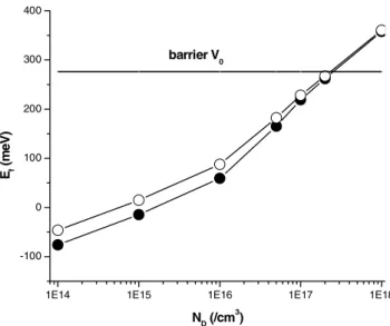
-100 0 100 200 300 400 barrier V0 Ef (m e V ) ND(/cm3)
Fig. 4 Quasi-Fermi level is shown as a function of the doping level in the absence (χ = 0, hollow circles) and presence (χ = 1, solid circles) of a test charge. The test charge is located at the center of the dot. The horizontal line represents the barrier height of V0.
ND is as low as 1014 cm3, the current model can lead to large errors because of the long tails of the
Cou-lomb potential. However, the probability of finding an electron in a QD is also small.
When the doping density is low (NiⰆ 1), i.e., the screening effects are negligible, how does a test charge affect the confinement energy levels Ej, j = 1, 2, 3 …, of a QD? Figure 1 shows Ej as a function of dot size c with a low doping density of ND = 1 × 1014 cm3. We discuss the cases of χ = 0 and χ = 1 with
xi = yi = zi = 0. (1) When there is no test charge (i.e. χ = 0), Ej are marked with hollow circles. Here, we
see that when c is less than 8 nm, dots are so small that there exists only one discrete level (Jd = 1), the ground state energy E1 (singlet). When c increases to between 8 and 10 nm, there are two discrete levels (Jd = 2) because the dots are now large enough to allow the existence of the 1st excited state E
2, which is
a triplet due to the cubic symmetry of the dot. When c is 10 nm and larger, there exists at least three discrete levels (Jd = 3) and E3 is a triplet because of the cubic symmetry, as indicated in Fig. 1. (2) When there is a test charge present (i.e. χ = 1), Ej are marked with solid circles. Here, we see that when c is less than 7 nm, there exists only the ground state energy E1 (singlet) with Jd = 1. When c increases to between 7 and 10 nm, we have Jd = 2, E1 (singlet) and E2 (triplet). When c is 10 nm and larger, there exists at least three discrete levels (Jd = 3), E1 (singlet), E2 (triplet) and E3 (triplet). Figure 1 shows that Ej with χ = 0 is always larger than Ej with χ = 1 because in the latter case, the QD includes a positive test charge with a negative Coulomb potential energy. Let ∆Ej = Ej (χ = 0) – Ej (χ = 1) be the energy shift of the j-th state due to the presence of a test charge. For c = 10 nm, Fig. 1 shows ∆E1 = 28.16 meV, ∆E2 = 20.75 meV and ∆E3 = 15.56 meV. Note that since the doping density is so low that there are only a few free elec-trons inside the dot, the screening effect due to many particle interactions is insignificant, and the band bending is negligible (i.e. Vp≈ 0). We discuss the screening effect and band bending in detail later. Fig-ure 2 shows the variation of the quasi-Fermi energy Ef with the dot size c for the cases of χ = 0 marked with hollow circles and χ = 1 with xi = yi = zi = 0 marked with solid circles. Here we see that Ef with χ = 1 is lower than Ef with χ = 0 because in the former case, Ej are lower. This result is a direct
conse-quence of the charge neutrality (see Eq. (8)).
Consider a dot with a side of c = 9 nm and two discrete energy levels (Jd = 2, see Fig. 1). We investi-gate how Ej and Ef vary with ND. Assume that there is a test charge located at xi = yi = zi = 0 if χ = 1. In Fig. 3, the ground state energy E1 and the first excited state energy E2 are marked with solid circles for χ = 1 and marked with hollow circles for χ = 0. When ND increases, E1 and E2 increase and when ND
is larger than 2 × 1018 cm3, E
-10 -8 -6 -4 -2 0 2 4 6 8 10 0 20 40 60 xi=yi=0 ND=1017/cm3 n/ ND z (nm) 4.5 no test charge
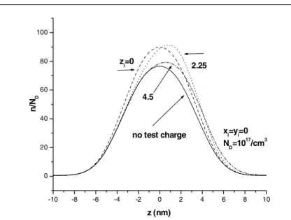
Fig. 5 Carrier density is shown as a function of the distance along the z-axis in the absence and in the presence of a test charge located along this axis. A cubic dot size c = 9 nm with a doping density ND = 1 × 1017 cm3. The three locations of the test charge are at zi = 0, 2, 25 and 4.5 nm.
doping levels, there are no states which are confined in the dot. Here, we observe that the energy shifts due to the test charge ∆Ej (= Ej (χ = 0) – Ej (χ = 1)) for j = 1 and 2 decrease sharply if ND is larger than 1016 cm3 as indicated in Fig. 3. The variation of the quasi-Fermi energy E
f with ND for χ = 0 marked with
hollow circles and χ = 1 marked with solid circles is plotted in Fig. 4. Here we see that when ND in-creases, the Fermi levels of χ = 0 and χ = 1 increase. When ND is larger than 2 × 1017 cm3, E
f is located in
the quasi-continuum levels in the barrier. However, when ND is small (1014 cm3), the charge neutrality
(Eq. (8)) implies that Ef must lie down below the ground state energy E1 and the probability of finding an electron in the ground state energy E1 is small.
We know that the distributions of the carrier density n(x, y, z) and the electrostatic potential energy Vp(x, y, z)must vary with the location (xi, yi, zi) of a test charge, and we discuss our result here. Consider
a cubic dot with a side of c = 9 nm uniformly doped with ND = 1 × 10¹⁷/cm3 and two discrete energy
levels (Jd = 2) as indicated in Fig. 1. Suppose that the location of a test charge zi is on the z-axis with xi = yi = 0. Figure 5 presents the variations of the carrier density n(0, 0, z) as a function of z for the case
of χ = 0 with a solid curve and for the case of χ = 1 with dashed curves when zi = 0, 2.25 and 4.5 nm. When there is no test charge (χ = 0) in the system, most of electrons accumulate around the center of the cube, and the distributition n as a function of z is expected to be symmetric because the QD possesses cubic symmetry.
When there is a test charge (χ = 1) located at the dot center (xi = yi = zi = 0), because of the attraction of the test charge, even more electrons accumulate around the dot center when compared with the case of χ = 0. When the test charge moves away from the center to zi = 2.25 nm, we see that a lot of electrons are
dragged along and move with the test charge, and n(0, 0, z) becomes asymmetric with respect to z. How-ever, when zi (= 4.5 nm) is too far away from the dot center, the Coulomb interaction between the con-finement carriers and the test charge becomes insignificant, and the distribution of n(0, 0, z) becomes similar to the distribution of n(0, 0, z) with χ = 0, as shown in Fig. 5. Variations of the electrostatic po-tential energy Vp(0, 0, z) for the case of χ = 0 with a solid curve and for the case of χ = 1 with non-solid curves at zi = 0,2.25 and 4.5 are plotted in Fig. 6. When there is no test charge, χ = 0, Vp is positive and Vp(0, 0, 0) can be as large as 80 meV because of the electron-electron interaction, and non-zero Vp leads
to a large band bending. When the test charge is located at the center of the dot (xi = yi = zi = 0), χ = 1, the test charge is strongly screened, leading to a screened Coulomb potential with a half width W of about 1 nm as indicated in Fig. 6. W is defined as z at |Vp|max minus z at (Vp = 0). The reason why the screening effect is strong is that not only most electrons are bunched near the dot center, but the test
phys. stat. sol. (b) 242, No. 14 (2005) / www.pss-b.com 2853 Paper -20 -15 -10 -5 0 5 10 15 20 -120 -100 -80 -60 -40 -20 0 20 40 60 80 100 Vp (m e V ) z (nm) 4.5 2.25 z i=0 no test charge xi=yi=0 ND=1017/cm3
Fig. 6 Electrostatic potential is shown as a function of the distance along the z-axis for the same circum-stances given in Fig. 5 for the carrier density (c = 9 nm and ND = 1 × 1017 cm3).
charge is also at the dot center and can easily attract a lot of electrons, as discussed in Fig. 5. When the test charge shifts away from the dot center, it moves away from the electron source, and the electron shielding thus falls off and Vp looks more like a long-range bare Coulomb potential, as illustrated in Fig. 6. The corresponding potential profiles are presented in Fig. 7. The potential profile Vpp is Vc + Vp. Here, we observe that Vpp(0, 0, z) is a square potential well marked with solid circles when there is no screening and no test charge included in the self-consistent calculation. When the electron–electron in-teraction is included without the test charge (χ = 0) in the calculation, band bending emerges as indicated by the solid curve in Fig. 7. If both the screening effect and the test charge are included in the calcula-tion, we see that when the test charge moves away from the dot center, the dip in Vpp not only moves away accordingly but also grows stronger and then diminishing. Figure 7 shows that when the screening effect is included in the calculation, the depths of the confinement potential energies for the case of χ = 1 (all dash curves) are effectively enhanced when compared with that for the case of χ = 0 (solid curve).
-20 -15 -10 -5 0 5 10 15 20 -150 -100 -50 0 50 100 150 200 250 300 350 no test charge no screening no test charge P o te nti a l P ro fi le (me V ) z (nm) 4.5 2.25 zi=0 xi=yi=0 x=y=0 ND=1017/cm3
Fig. 7 Potential profile Vpp = Vc + Vp is shown as a function of the distance along the z-axis for the case of no screening and for the case of screening both in the absence and presence of a test charge. The loca-tions of the test charge are the same as given in Figs. 5 and 6 (c = 9 nm and ND = 1 × 1017 cm3).
0 4 8 12 16 20 80 90 100 110 120 ND=1x10¹⁴/cm3 xi=yi=0 E1 (me V ) zi(nm)
Fig. 8 Ground state energy E1 is shown as a function of the test charge’s location along the z-axis for doping concentrations ND = 1 × 1014 cm3 and N
D = 5 × 1016 cm3.
Finally, we discuss the variation of Ej and Ef with the location of a test charge. Consider a dot with a side of c = 9 nm where there are two energy levels (Jd = 2, see Fig. 1). The ground state energy E1 as a function of the test charge’s location zi along the z-axis with xi = yi = 0 for ND = 1 × 1014 cm3 and
ND = 5 × 1016 cm3 is presented in Fig. 8. When the test charge moves within 2 nm (i.e., ≈2 W as
dis-cussed in Fig. 6) from the center, E1 is almost constant, but when zi is larger than 2 nm, E1 increases moderately and reaches the asymptotic values of 112 meV for ND = 1 × 1014 cm3 and 149 meV for
ND = 4 × 1016 cm3, respectively. When zi is larger than 16 nm or so, the Coulomb interaction between the
confined carriers and the test charge is negligible. The asymptotic values reported above are the screened ground state energies of a QD without a test charge (χ = 0) and are consistent with those values shown in Figs. 1 and 3. Variation of Ef as a function of zi with ND = 1 × 1014 cm3 and N
D = 5 × 1016 cm3 is plotted in
Fig. 9. For both cases, Ef increases and levels off as zi increases.
0 4 8 12 16 20 -100 -50 0 50 100 150 200 xi=yi=0 ND=1x10¹⁴/cm3 ND=5x10¹⁶/cm3 Ef (me V ) zi(nm)
Fig. 9 Quasi-Fermi level Ef is shown as a function of the test charge’s location along the z-axis for dop-ing concentrations ND = 1 × 1014 cm3 and N
phys. stat. sol. (b) 242, No. 14 (2005) / www.pss-b.com 2855
Paper
4 Summary
We have formulated a self-consistent calculation of the energy levels, quasi-Fermi energy and potential energy profiles in a cubic quantum dot which takes both doping and the presence of a positive test charge into account. The calculation involves a self-consistent solution of Poisson’s equation and the Schrödinger equation. Our results show that both the energy levels and quasi-Fermi level in the dot in-crease with increasing doping and dein-crease when there is a positive test charge present. With very high doping the Fermi level is located in the barrier while with low doping the Fermi level is located down below the ground state energy which implies that the probability of finding an electron in a super-cell is very small. We have also found that at high doping levels, the lowest energy electron states are not con-fined in the dot. The carrier density in the dot is symmetric in the absence of the test charge, and in the case where the test charge is at the center of the dot. In the latter case, the carrier density is increased at the center of the dot as the positive test charge attracts more carriers to the center. When the test charge is displaced from the center of the dot, the carrier density becomes asymmetric about the center because of the attraction of the test charge. The potential profile Vpp is a square well potential at low doping densi-ties but shows strong band bending effects at higher doping densidensi-ties. The potential profile becomes strongly asymmetric when there is a test charge that is displaced from the center of the dot.
Acknowledgement One of the authors, Wu Ching Chou, acknowledges the support of the National Science Coun-cil of Taiwan under the grant numbers of NSC92-2112-M-009-041.
References
[1] N. Kirstaedter, O. G. Schmidt, N. N. Ledentsov, D. Bimberg, V. M. Ustinov, A. Yu. Egorov, A. E. Zhukov, M. V. Maximov, P. S. Kop’ev, and Zh. I. Alferov, Appl. Phys. Lett. 69, 1226 (1996).
[2] P. M. Petroff, A. C. Gossard, R. A. Logan, and W. Wiegmann, Appl. Phys. Lett. 41, 635–638 (1982).
[3] F. E. Prins, G. Lehr, M. Burkard, H. Schweizer, M. H. Pilkuhn, and G. W. Smith, Appl. Phys. Lett. 62, 1365–1367 (1993).
[4] M. A. Reed, R. T. Bate, K. Bradshaw, W. M. Duncan, W. M. Frensley, J. W. Lee, and H. D. Smith, J. Vac. Sci. Technol. B 4, 358 (1986).
[5] P. M. Petroff and S. P. Denbaars, Superlattices Microstruct. 15, 5 (1994). [6] Y. Nabetani, T. Ishikawa, S. Noda, and A. Sakai, J. Appl. Phys. 76, 347 (1994).
[7] N. N. Ledentsov, V. A. Shchukin, M. Grundmann, N. Kirstaedter, J. Böhrer, O. Schmidt, D. Bimberg, V. M. Ustinov, A. Yu. Egorov, A. E. Zhukov, P. S. Kop’ev, S. V. Zaitsev, N. Yu. Gordeev, Zh. I. Alferov, A. I. Borovkov, A. O. Kosogov, S. S. Ruvimov, P. Werner, U. Gösele, and J. Heydenreich, Phys. Rev. B 54, 8743 (1996).
[8] S. P. Guo, X. Zhou, O. Maksimov, M. C. Tamargo, C. Chi, A. Couzis, C. Maldarelli, I. L. Kuskovsky, and G. F. Newmark, J. Vac. Sci. Technol. B 19, 1635 (2001).
[9] B. Damilano, N. Grandjean, F. Semond, J. Massies, and M. Leroux, Appl. Phys. Lett. 75, 962 (1999). [10] M. Klude, T. Passow, H. Heinke, and D. Hommel, phys. stat. sol. (b) 229, 1029 (2002).
[11] B. Kato, H. Noguchi, M. Nagazi, H. Ohkuyama, S. Kijima, and A. Ishibashi, Electron. Lett. 34, 282 (1998). [12] J. Lee, M. O. Vassell, and G. J. Jan, IEEE J. Quantum Electron. 4, 1469 (1993).
[13] J. Lee and M. O. Vassell, IEEE Photon. Technol. Lett. 4, 1222 (1992). [14] S. L. Chuang, Physics of Optoelectronic Devices (Wiley, New York, 1955). [15] S. Gangopadhyay and B. R. Nag, Nanotechnology 8, 14 (1997).
[16] D. Gershoni, H. Temkin, G. J. Dolan, J. Dunsmuir, S. N. G. Chu, and M. B. Panish, Appl. Phys. Lett. 53, 995 (1988).
[17] J. Shertzer and L. R. Ram-Mohan, Phys. Rev. B 41, 9994 (1990).
[18] M. A. Cusack, P. R. Briddon, and M. Jaros, Phys. Rev. B 54, R2300 (1996). [19] M. Grundmann, O. Stier, and D. Bimberg, Phys. Rev. B 52, 11969 (1995). [20] O. Stier, M. Grundmann, and D. Bimberg, Phys. Rev. B 59, 5688 (1999). [21] A. J. Williamson and Alex Zunger, Phys. Rev. B 59, 15819 (1999).