國 立 交 通 大 學
電子工程學系電子研究所碩士班
碩 士 論 文
一維氧化鋅/二氧化鈦核殼結構奈米線之光學與場
發射特性研究
Field Emission and Optical Properties of 1D
ZnO/TiO
2Core-shell Nanowires
研 究 生:陳冠仲
指導教授:曾俊元
中華民國九十六年六月
一維氧化鋅/二氧化鈦核殼結構奈米線之光學與場
發射特性研究
Field Emission and Optical Properties of 1D
ZnO/TiO
2Core-shell Nanowires
研 究 生 : 陳冠仲 Student: Guan-Zhong Chen 指導教授 :曾俊元 教 授 Advisor: Prof. Tseung-Yuen Tseng
國 立 交 通 大 學
電子工程學系電子研究所碩士班 碩 士 論 文
A Thesis
Submitted to Department of Electronics Engineering & Institute of Electronics
College of Electrical and Computer Engineering National Chiao Tung University
in partial Fulfillment of the Requirements For the Degree of
Master in
Electronics Engineering June 2007
一維氧化鋅/二氧化鈦核殼結構奈米線之光學與
場發射特性研究
研究生:陳冠仲 指導教授:曾俊元
國立交通大學
電子工程學系 電子研究所
摘要
本論文主要探討以氧化鋅及二氧化鈦型成合殼結構奈
米線,在低溫的環境中利用水熱法來形成氧化鋅奈米線當作
核,再藉由濺鍍沉積法形成二氧化鈦殼層。藉由改變水熱法
中的化學溶液濃度、成長時間來得到適當長度和密度的氧化
鋅奈米線。再藉由改變濺鍍的溫度、時間和功率來得到均勻
且不同厚度的二氧化鈦殼層,最後再利用濕式蝕刻法去除氧
化鋅奈米線來製備空心二氧化鈦奈米管。並探討氧化鋅/二
氧化鈦核殼結構奈米線的光學特性、晶體結構、表面型態及
場發射特性,同時分析其加熱處理後對此結構的影響。
Field Emission and Optical Properties of 1D
ZnO/TiO
2Core-shell Nanowires
Student: Guan-Zhong Chen Advisor: Tseung-Yuen Tseng
Department of Electronics Engineering and Institute of Electronics National Chiao Tung University
Abstract
In this thesis, 1D ZnO/TiO2 core-shell nanowires were prepared in
two steps process. ZnO nanowires were fabricated by hydrothermal method at the low temperature as core. The ZnO nanowires were fabricated under the various solution concentrations and growth times of hydrothermal method in order to get a suitable ZnO nanowries array.
TiO2 shell was deposited by sputtering method under the various
sputtering time and power to get a uniform and different thickness. TiO2
誌謝
首先誠摯的感謝指導教授曾俊元博士,老師悉心的教導使我得以 一窺固態電子領域的深奧,不時的討論並指點我正確的方向,使我在 這些年中獲益匪淺。老師對學問的嚴謹更是我輩學習的典範。 本論文的完成另外亦得感謝承佑、永昇和志洋學長的大力協助。 因為有你們的意見和分析,使得實驗的過程中因而順利且完整。 兩年裡的日子,實驗室裡共同的生活點滴,學術上的討論、敗戰 隊友遠永都不離不棄、義氣到底的革命情感、因為偷懶睡太晚而衝衝 忙忙閃進實驗室...,感謝眾位學長姐、同學、學弟妹的共同砥 礪,你/妳們的陪伴讓兩年的研究生活變得絢麗多彩。 感謝家瑋、信賢、群傑、孟漢、聖裕等學長及秀玉和佳穎學姐的 指導和費心,鎮宇、重毅、俊勝、俊興、士傑、松蒔和我共同努力及 成長,以及毅函、世偉、啟翔和宏全你們的陪伴讓這兩年的研究生活 變得絢麗多彩。 最後更感謝我的父母,默默地支持和栽培使我能完成這段歷程, 這份喜悅禮是屬於你們的。Contents
Chinese Abstract ... I Abstract... II Acknowledgement...III Contents ... IV List of Illustrations... VI List of Tables ... IX Chapter 1 Introduction ...1 1.1 Nanostructures ... 1 1.2 ZnO Characteristics ... 21.2.1 The Growth Methods of ZnO Nanowires ... 3
1.2.2 The Optical Properties... 7
1.3 TiO2 Characteristics... 12
1.4 Core-shell Structures ... 14
1.5 Field-Emission Properties... 16
Chapter 2 Experiment Details ...18
2.1 The Process Flow of Experiment ... 18
2.2 Sample Preparation... 19
2.2.1 Wafer Clean... 20
2.2.2 Deposition of ZnO Seed Layer ... 20
2.2.3 Growth ZnO Nanowires Array... 22
2.2.4 Synthesized of ZnO/TiO2 Core-shell Structures... 23
2.2.5 Synthesized TiO2 Nanotubes... 24
2.3 Measurement Equipment... 25
2.3.1 Field Emission Scanning Electron Microscopy (FE-SEM) ... 25
2.3.2 High Resolution Transmission Electron Microscopy (HR-TEM) and Disersive X-Ray Energy (EDX)... 26
3.2 ZnO Nanowires... 35
3.2.1 Characterization of ZnO Nanowires ... 36
3.2.2 The Optical Properties... 42
3.2.3 The Field Emission Properties ... 45
3.3 ZnO/TiO2 Core-shell Nanowires ... 49
3.3.1 The Field Emission Scanning Electron Microscopy Analyses . 49 3.3.2 The High Resolution Transmission Electron Microscopy and Disersive X-Ray Energy Analyses... 53
3.3.3 The X-Ray Diffraction Analyses ... 56
3.3.4 The Optical Properties... 59
3.3.5 The Field Emission Properties ... 62
3.4 TiO2 Nanotubes... 67
3.4.1 The Field Emission Scanning Electron Microscopy analyses .. 67
3.4.2 The High Resolution Transmission Electron Microscopy Analyses and Disersive X-Ray Energy... 68
List of Illustrations
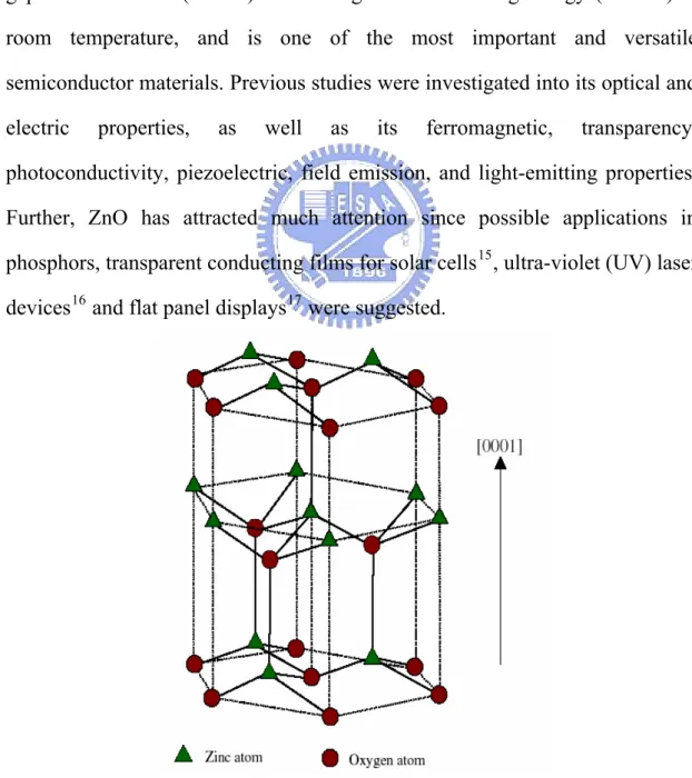
Figure 1-1. Wurtzite structure of ZnO. 2
Figure 1-2. VLS process. 4
Figure 1-3. The schematic geometry of ZnO nanowires growth. 1. Furnace tube, 2. slender tube, 3. source, 4. template, 5. alumina supporter 4 Figure 1-4. The growth process of the ZnO nanowires by the hydrothermal
method. 6
Figure 1-5.The mechanism of the photoluminescence. 8 Figure 1-6. The draft of the calculated defect`s levels in ZnO film. 9 Figure 1-7. Schematic showing the energy-band diagram of a ZnO grain in
cross section. The conduction band (Ec), valance band (Ev), Fermi level (EF), paramagnetic oxygen vacancy (VO*) level, and the
diamagnetic VO** area (hatched) in the grain-boundary depletion
region are visualized for a grain with a (a) low and (b) high
free-carrier density. The circles and arrows symbolize electron–hole recombination events which emit green light. 11 Figure 1-8. Band bending of nanowires. 16 Figure 2-1. The structure of ZnO nanowires arrary. 22 Figure 2-2. The structure ZnO/TiO2 core-shell. 23
Figure 2-3.TiO2 nanotubes was fabricated by wet-etching (a) 30 min (b) 60
min. 24 Figure 2-4.Schematic diagram of a high-vacuum chamber system for field
emission property measurement. 29 Figure 3-1. SEM image of ZnO nanoflowers. 31 Figure 3-2. The SEM image of ZnO seeding layer on the Si substrate. (a)
Figure 3-7. Aspect ratio of ZnO nanowires as a function of concentration. 38 Figure 3-8. (a) Cross-section FE-SEM micrographs of ZnO nanowires at
0.0125 M with growing 60min (b) 75 min (c) 90 min (d) 105 min (e)120 min (f) 150 min (g) 180 min. 40 Figure 3-9. Average length of ZnO nanowires as a function of growth time.
41 Figure 3-10. The X-ray diffraction pattern of ZnO nanowires grown on Si
wafer with different growth time (a) 70 min (b)120 min. 41 Figure 3-11. The CL spectra of ZnO nanowires for 70min and 120 min. 43 Figure 3-12. The CL spectra of ZnO nanowires as growth and after
annealing. 44 Figure 3-13. Field emission current-voltage curves of ZnO nanowires with
different growth time. 46 Figure 3-14. The Fowler-Nordhiem (F-N) plots of ZnO nanowires with
different growth time 47 Figure 3-15. SEM images of ZnO/TiO2 core-shell nanowires deposited at
room temperature. 50 Figure 3-16. SEM images of ZnO/TiO2 core-shell nanowires with different
sputter arameters. 52 Figure 3-17. The TEM micrographs of (a) ZnO/TiO2 core-shell structure.
(b) region A (c) region B (d) region C. (e) The HR-TEM micrographs of region A (d) SAED spectra of region A. 54 Figure 3-18. The XRD patterns of ZnO/TiO2 core-shell structure with
various sputtering power, time (a) as TiO2 deposition, (b) after
annealing 400 1 hour in air, (c) after annealing 500 1 hour in air.℃ ℃
58 Figure 3-19. CL spectra of ZnO nanowires and ZnO/TiO2 core-shell
nanowires as deposited. 60 Figure 3-20. (a) CL spectra of ZnO nanowires and ZnO/TiO2 core-shell
nanowires after annealing 400 (b) 500 1 hour under the air.℃ ℃ 61 Figure 3-21.Schematic energy level diagram of a ZnO/TiO2 core-shell
structure. 62 Figure 3-22. (a) Field emission current-voltage curves of ZnO/TiO2
core-shell nanowires as deposited. (b) The F-N plot of ZnO/TiO2
core-shell nanowires as deposited. 63 Figure 3-23. (a) Field emission current-voltage curves of ZnO/TiO2
core-shell nanowires after annealing. 65 Figure 3-24. The SEM image of ZnO/TiO2 core-shell nanowires after wet
etching 30 min (a) top view (b) cross section. 68 Figure 3-25. The TEM micrographs of (a) TiO2 tube. (b) region B (c)
SAED spectra of region B. 70 Figure 3-26. The TEM micrographs of (a) ZnO/TiO2 nanowire. (b) region
B. 72 Figure 3-27. SAED spectra of (a) region B (b) region C. 73
List of Tables
Table 1-1.Typical physical and mechanical properties of titania. 12 Table 3-1. The detail data of field emission property of ZnO nanowires
with different growth time. 48 Table 3-2. The atomic percentage of ZnO/TiO2 core-shell structure
analyses by EDX. 55 Table 3-3. The detail data of field emission property of ZnO/TiO2
core-shell nanowires as deposited. 64 Table 3-4. The detail data of field emission property of ZnO/TiO2
core-shell nanowires after annealing. 66 Table 3-5. The atomic percentage of ZnO/TiO2 core-shell structure
analyses by EDX. 70 Table 3-6. The atomic percentage of ZnO/TiO2 core-shell structure
Chapter 1 Introduction
1.1
Nanostructures
Recently, nanotechnology had been research extensively. Nanostructures can be defined as systems in which at less one dimension is smaller than 100 nm where new physical, chemical and biological properties occur as compared to bulk materials. There are many kinds of nanostructure, including one dimension (1D) nanostructure such as nanowire1, nanotube2 3 4, nanorods5 6 7; two dimension (2D) nanostructure such as nanoblet8 , nanosheets9 10 , nanoplanes; three dimension (3D) nanostructure such as nanoflower11, tetrapod nanorod12, nanoparticle13. Because of the specially electronic and optical properties of nanostructures they have high potential in application of the electron and optical devices. For example, nanodot was applied in nonvolatile memory, nanorods in field emission, nanowires in solar cell, etc.
Since the carbon nanotubes (CNTs) were discovered in 199114, the one dimension (1D) nanostructures were attracted a lot of attention. Except carbon, many materials were researched to use in nanodevices, like ZnO, GaAs and TiO2 etc. The Ⅲ-Ⅴ group semiconductor are always used for light emitting
1.2 ZnO Characteristics
Zinc oxide (ZnO) is a II-VI group semiconductor, has a stable wurtzite structure (Figure 1-1) with lattice spacing a = 0.325 nm and c = 0.521 nm. The ratio of c/a is 1.633 which is nearly perfect. It has high melting point (1975℃) and high thermal stability. Its molecular mass is 81.39. Its specific heat is 0.125 cal/gm. And its thermal conductivity is 0.006 cal/cm/K. ZnO is a wide band gap semiconductor (3.37ev) with a large exciton binding energy (60meV) at room temperature, and is one of the most important and versatile semiconductor materials. Previous studies were investigated into its optical and electric properties, as well as its ferromagnetic, transparency, photoconductivity, piezoelectric, field emission, and light-emitting properties. Further, ZnO has attracted much attention since possible applications in phosphors, transparent conducting films for solar cells15, ultra-violet (UV) laser devices16 and flat panel displays17 were suggested.
Since the first report of ultraviolet lasing from ZnO nanowires, nanostructure of ZnO has stimulated intensive research. Indeed, ZnO nanostructures are interesting to study not only the property of UV lasing emission in nanowire form, but also because a wide variety of morphologies have been prepared. Some kinds of the ZnO nanostructures contain nanowire, nanorod, nanosheet, nanoribbon, nanotube, nanoplate, tetrapod, and flower-liked structures. Indeed, based on the nano-scale structure on interface, those applications of morphological properties will exceed normal expectations and behave prominent effect.
Moreover, the high melting point, excellent chemical stability and small electron affinity which are the requirements to be an ideal anode material for field emission (FE) have made ZnO a perfect candidate for carbon nanotubes (CNTs) in the field emission.
1.2.1
The Growth Methods of ZnO Nanowires
There are a lot of methods of synthesizing ZnO nanowires such as VLS (vapor-liquid-solid) method, metal-organic chemical vapor deposition, thermal evaporation, electro-chemical deposition, template enhancement method, and hydrothermal method.
reaction temperature, the ZnO react with graphite to form Zn(g) and CO(g). The gaseous products produced by reactions (1) and (2) would adsorb and condense on the metal catalytic droplets. And then followed by nucleation and growth of single crystalline ZnO nanowires (Figure 1-2) following by the reaction (3). The corresponding chemical reaction can be shown in Figure 1-3.
ZnO(s) + C(s) Æ Zn(g) + CO(g) , (1)
CO(g) + ZnO(s) Æ CO2(g) + Zn(g) . (2)
Zn(g) + CO(g) Æ ZnO(s) + C(s) , (3)
C(s) + CO2(g) Æ 2CO(g) . (4)
Figure 1-2. VLS process.
Figure 1-3. The schematic geometry of ZnO nanowires growth. 1. Furnace tube, 2. slender tube, 3. source, 4. template, 5. alumina supporter
Various vapor-phase methods such as the vapor-liquid-solid epitaxial (VSLE), pulsed laser deposition (PLD), and metal-organic chemical vapor deposition (MOCVD) have been successfully used to grow oriented ZnO
nanowire arrays at temperatures of 800-900°C. In order to lower the temperature of the growing process, the ZnO nanowire can dope some impurities like tin (Sn) and indium (In). It can low the temperature of the growth about 500-600℃. The VLS (vapor-liquid-solid) method needed catalysts like aurum (Au) and copper (Cu). The control of the flow rate was very important. It affected the length, diameter and the density of the ZnO nanowires.
The template method19
The template method is that the porous Anodic Aluminum Oxide (AAO) substrate was used as a template to synthesize the ZnO nanowires. The AAO structure would provide some properties for nanowires, including high pores density, controllable diameter and length of pores, large area and high uniform. It can use many methods like CVD, sol-gel and hydrothermal method to fill the hole of the AAO template. After filling the ZnO, use NaOH solution to remove the AAO template and the ZnO nanowires remain on the substrate. It is easy and cheap to synthesize ZnO nanowires, but it has impurity problems and hard to create single crystal ZnO nanowires.
C-orientation was put into an aqueous solution of the zinc nitrate hexahydrate ( Zn(NO3)2.6H2O (99.9% purity)) and the hexa-methylenetetramine (HMTA;
C6H12N4, (99.9% purity)) in a sealed vessel. Zinc nitrate hexahydrate is used as
source of zinc and hexamethylenetetramine is used to control the PH value. These can be represented by the following reactions:
(CH2)6N4 + 6H2O → 6HCHO + 4NH3 (5)
NH3 + H2O ↔ NH4+ + OH- (6)
2OH- + Zn2+ → Zn(OH)2 (7)
Zn(OH)2 → ZnO(s)+ H2O (8)
The hydrothermal method is involved two steps as nucleation and growth. When zinc nitrate hexahydrate and hexa-methylenetetramine are mixed together, no precipitation accrues initially. With the increase of temperature, the HMTA begins to decompose into ammonia and then Zn(OH)2 occurred.
The precipitation appeared quickly. And then ZnO nuclei are formed on the substrate. After the ZnO film grows from the nuclei, the ZnO nanowires begin to grow. The growth process is shown in Figure 1-4.
Figure 1-4. The growth process of the ZnO nanowires by the hydrothermal method.
So the synthesis of one-dimensional ZnO nanostructures by wet chemical approach without involving catalysts or templates provides a promising option
for the large-scale production of well-dispersed one-dimensional nanostructured materials .
1.2.2
The Optical Properties
Recently, ZnO have been used in optical application widely, such as ultraviolet laser. ZnO is a well-known semiconductor for its wide band gap and high exciton binding energy at room temperature.
The strong exciton binding energy of ZnO (~60 meV) is much larger than that of ZnSe (~22 meV) and GaN (~25 meV), also larger than the thermal energy of ZnO (~26 meV), which are favorable for obtaining an efficient excitonic laser action at room temperature. So ZnO is a good candidate for blue-UV emission optoelectronic devices.
Zinc oxide (ZnO) generally had two kinds of emission manner. One was the ultraviolet emission, the other was the green emission. The ultraviolet emission was related to the exciton emission of ZnO. The mechanism of the emission is shown in Figure 1-5. The green emission was related that the electron transition from valence band to the energy band of impurity. If the component, structure and defects changed, the characterization of emission changed23.
Ec Ev Eex Eg Ed Photon or heat
: electron
: hole
Figure 1-5.The mechanism of the photoluminescence.
The green emission24 (519 nm) originates from the oxygen vacancies according to the result of Vanheusden et al.25. By full-potential linear muffin-tin orbital method, the green emission of ZnO is because that the oxygen interstitials (Oi) occupy the zinc vacancies (VZn) to form the defect of
antisite oxide (OZn). The kind of defect is easily formed because the ant site
oxide has relatively low formation energy. It is shown in Figure 1-6. All the prepared films are n-type and the majority donors are oxygen vacancies (VO)
and zinc interstitials (Zni). It is proved that the singly ionized oxygen vacancy
is responsible for the green emission and this emission results from the recombination of a photogenerated hole with a singly ionized charge state of this defect. The more singly ionized oxygen vacancies there are, the stronger the luminescence intensity is.26
Figure 1-6. The draft of the calculated defect`s levels in ZnO film.
The mechanism of the photoluminescence is that the photon excited the electrons from valence band to excited state of ZnO. And then electrons and holes recombine together to release the photon, heat or another form of energy. The exciting energy must be higher than the energy level of ZnO. The illuminant energy is absorbed by electrons of the sample and then electrons will jump to higher level. After that it would spontaneously jump to the low level. And then release the energy in the form of light. When there exists another energy state between excited state and the valence band, for example: donor level or accepter level. The electrons jump from the valence band to the excited state and then jump from the excited state to donor level or accepter level and
not recombine with the holes in the valence band. So they make luminescence efficiency reduce and influence the power of intensity.
Oxygen vacancies in ZnO can occur in three different charge states:the VΦ state which has captured two electrons and is neutral relative to the lattice,
the singly ionized VO * state, and the VO ** state which did not trap any electron
and is doubly positively charged with respect to the lattice. The VΦ state is
Figure 1-7. Schematic showing the energy-band diagram of a ZnO grain in cross section. The conduction band (Ec), valance band (Ev), Fermi level (EF),
paramagnetic oxygen vacancy (VO*) level, and the diamagnetic VO** area
(hatched) in the grain-boundary depletion region are visualized for a grain with a (a) low and (b) high free-carrier density. The circles and arrows symbolize electron–hole recombination events which emit green light.
1.3
TiO
2
Characteristics
28
Titanium dioxide, also known as titanium (IV) oxide or titania, is the naturally occurring oxide of titanium, chemical formula TiO2. Titanium dioxide
exists in a number of crystalline forms including Rtile, Aatase, Bookite, Titanium dioxide (B) or TiO2(B). Rtile and Aatase are most important
crystalline formsin in the electronic industry. There are physical and mechanical properties of TiO2 in the Table 1-1.
Density
4 gcm-3 Anatase : 3.84 gcm-3 Rtile : 4.26 gcm-3
Porosity 0% Modulus of Rupture 140MPa
Compressive Strength 680MPa Poisson’s Ratio 0.27 Fracture Toughness 3.2 Mpa.m-1/2
Shear Modulus 90GPa Modulus of Elasticity 230GPa Microhardness (HV0.5) 880 Resistivity (25°C) 1012 ohm.cm Resistivity (700°C) 2.5x10⁴ ohm.cm Dielectric Constant (1MHz) 85 Dissipation factor (1MHz) 5x10⁻⁴ Dielectric strength 4 kVmm-1 Thermal expansion (RT-1000°C) 9 x 10⁻⁶ Thermal Conductivity (25°C) 11.7 WmK-1 Refractive Index Anatase : 2.46
Rtile : 2.903 Crystal Structure Anatase : Tetragonal
Rtile : Tetragonal Table 1-1.Typical physical and mechanical properties of titania.
Nanosized titanium dioxide (TiO2) structures have been the subject of a
applications in the areas of pigments29, gas sensors, catalysis, photocatalysts30, photovoltaics31, optics, inorganic membranes, filed emission32and dielectric materials. It is not surprising in view of the importance of TiO2 nanostructures
that a wide variety of approaches for the synthesis of nanosized TiO2 have been
1.4
Core-shell Structures
33
In recent years, there has been interest surrounding the fabrication of core–shell structures that consist of templated cores coated with shells of different chemical composition. These core–shell structures often exhibit properties that are different from those of the templated cores (for example, increased stability, higher surface area, and different magnetic and optical properties), thus making them attractive from both scientific and technological viewpoints34. Furthermore, the properties of core–shell particles can be also tailored in a controllable fashion by independently altering the composition, dimension, and structure of the core or shell. Applications for such core–shell spheres are diverse, including solar cell35, optical resonance engineer36, photonic crystal37, biosensor38, etc.
In general there are many kind methods to synthesize nanosize core-shell structures the most important of which are polymer, inorganic and biomacromolecule coating methods. Now we focus of the inorganic coating methods. At 2006s, Chen et al.11 has succeed to synthesize the amorphous titania-coated zinc oxide nanoparticles core-shell structures by two step process. First, ZnO nanoparticles were prepared by the solvothermal synthesis in ethanol. And then ZnO nanoparticles were coated with amorphous TiO2 via a
sol-gel process. And they reported that TiO2 shell thickness on the surface of
ZnO nanoparticles was very important in the enhancement of PL intensity. At 2005s, Zheng et al.12 had fabricated T-ZnO/SnO2 core-shell nanorods. Zinc
powder was heated on the silicon wafer with oxygen flow to prepare the T-ZnO nanorods. The as-grown T-ZnO nanorods was heated to the desired temperature (typically T = 770 °C) with SnH4/N2 flow. The products,
T-ZnO/SnO2 core-shell heterostructures were accomplished. At 2006s, Yang et
al.35 used ZnO-Al2O3 and ZnO-TiO2 Core-Shell Nanowire to synthesize
dye-sensitized solar cells. They grew ZnO nanowires as the core by hydrothermal method. Shells of Al2O3 or TiO2 were deposited on the nanowires
films by atomic layer deposition (ALD) process.
1.5
Field-Emission Properties
It is well know that high aspect ratio and sharp tip nanostructures like nanowires, nanotubes and nanorods are suitable for cold cathode field emission application. When negative voltage was applied on nanowires, the negative voltage would induce a high electric field on the tip of structures. The high electric field will let the potential barrier narrow as shows in the Figure 1-8. If the potential barrier is narrow enough, electrons would pass through the barrier as result in the current.
Figure 1-8. Band bending of nanowires.
This phenomenon we also know as Fowler-Nordheim tunneling. This phenomenon is highly dependent on both properties of the material and the shape of the particular cathode, so that higher aspect ratios produce higher field emission currents. This field emission current density can be described by the F-N equation. The F-N equation is as follow:
Fowler-Nordheim (F-N) equation : 3 2 2 2
exp[
]
J
β
β
Α Ε
ΒΦ
=
−
Φ
Ε
[1.1]10 2 1.56 10 (− AV eV− ) Α = × [1.2] 3 3 2
6.83 10 (
eV V um
−)
Β =
×
[1.3]Where J is the current density, E is the applied electric field of tip, is the work function (ev), βis the field emission enhancement factor, A and B are canstants. The logarithmic form of Eq. [1.1] can be expressed as follow:
Φ 3 2 2 2 1 ln( J ) ln( β ) β ΒΦ Α = − + Ε Ε Φ [1.4]
A plot of log(J/E2) versus 1/E will be a straight line with slop m and intercept b. Slop m and intercept b is gived by follow:
3 2
m
β
ΒΦ
= −
[1.5] 2ln(
)
b
=
Α
β
Φ
[1.6]The value β can be calculated by the F-N plot. The β value presents the field emission effect well or not. In other words high β value represents a strong field emission mechanism; low β value means a poor field emission mechaism. Besides, it is well know that the β value only depends on geometry,
Chapter 2 Experiment Details
2.1 The Process Flow of Experiment
2.2 Sample Preparation
2.2.1 Wafer Clean
In the experiment, the p-type Si (100) substrate was cleaned by a standard Radio Corporation of America (RCA) cleaning method and rinsed in acetone for 30 min. to remove native oxide from the surface of Si substrate.
2.2.2 Deposition of ZnO Seed Layer
The ZnO seed layer which can help to grow well-aligned ZnO nanowires was deposited by Radio frequency (RF) magnetron sputtering system. The Sputtering system can divided into five parts.
Vacuum system:
It contains a mechanical pump for rough vacuum, a diffusion pump for high vacuum, and three valves to control the vacuum pressure in chamber and in tubes.
Pressure system
There are two digital gauges in pressure system. One is Granville-Phlips Co.’s product, which provides an accuracy of 0.1m torr with a display range from 1 ATM to 0.1m torr to show the chamber pressure condition for low vacuum. And the other is an ion gauge, which would show the pressure condition of high vacuum from to torr. Accordingly, we can monitor the vacuum situation in sputter chamber under sputtering, through these two machines.
3
10− 10−7
Generally speaking, the content of oxygen plays an important role in oxide ceramics. So we utilize Gas MFC (mass flow meter) to control the flow rate and atmosphere ratio during thin film deposition process in order to exam the atmosphere ratio dependence.
Plasma controlling system
We set the system, which involves a RF power generator, an automatic network-matching box, a 2-inch magnetron gun and its shutter and 2-inch one to produce plasma. The power generator can provide the maximum power of 600 W (13.56MHz), besides, the automatic network-matching box can adjust the capacitances of the total network for minimum reflection power. Consequently, we are able to adjust the power magnitude to modify our process.
Cooling system
The recurring water circling sputter machine is driven by pump for cooling all system.
The ZnO seeding layer was deposited on Si wafer under 10 mtorr Argon (Ar) and Oxygen (O2) flow ratio 3:1 using home made ZnO target with 30W
After the milling, put it in the 2.5 inch pattern and press the pattern to 15000 p.s.i. for 1 min. Finally, the stressed powders were put into the oven to sinter at 1300 for 4 hours. After sintering, grind the target into 2 inch in diameter. ℃ Then plaster the ZnO target and copper plate with Ag glue and put into the oven to sinter for 1 day.
2.2.3 Growth ZnO Nanowires Array
The Si substrate with ZnO seeding layer was put into an aqueous solution of zinc nitrate hexahydrate (Zn(NO3)2 . 6H2O, (99.9%)) and
hexamethylenetetramine ( HMTA ; C6H12N4, (99.9 %)) in a sealed vessel at 95
℃ for various reaction times from 10 min to 150 min. The concentration of zinc and amine were fixed at 0.0125 M. The structure was as below ( Figure 2-1).
ZnO nanowires
Silicon substrate
Polycrystalline ZnO seeding layer
ZnO nanowires
Silicon substrate
Polycrystalline ZnO seeding layer
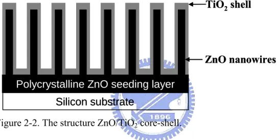
2.2.4 Synthesized of ZnO/TiO
2Core-shell Structures
The TiO2 shell was deposited on ZnO nanowires by rf sputtering (13.56
MHz) under 10 mtorr Argon and Oxygen flow ratio 1:1 using home made TiO2
target with vary sputtering power and time at 150 . After TiO℃ 2 was deposited,
use the oven to anneal the ZnO/TiO2 core-shell structure at 400 and 500 ℃ ℃
for 1 hour in the air. The structure was showed at Figure 2-2.
Silicon substrate
ZnO nanowires
Polycrystalline ZnO seeding layer
TiO
2shell
Silicon substrate
ZnO nanowires
Polycrystalline ZnO seeding layer
TiO
2shell
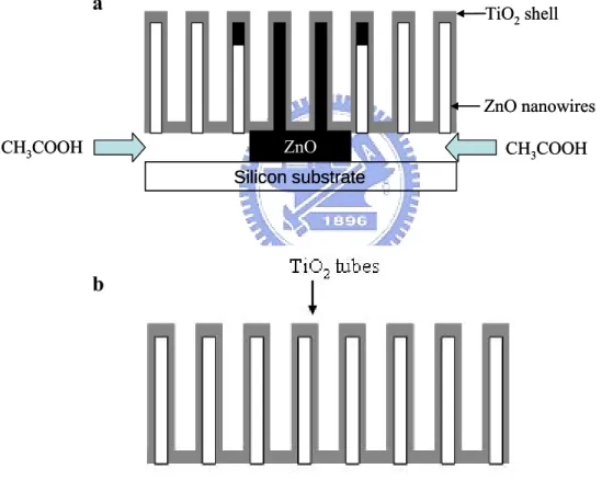
2.2.5
Synthesized TiO
2Nanotubes
After the ZnO/TiO2 core-shell structure nanowires were formed, the TiO2
nanotubes was fabricated by wet-etching process. The ZnO nanowires were etched by the acetic acid (H2O:CH3COOH = 1000:1) for 30 min and 60 min.
Beside, TiO2 had very slow etch rate of acetic acid. So after the etch process
the tubes- liked TiO2 shell were still residual on the substructure. The structure
was showed at Figure 2-3.
Silicon substrate ZnO nanowires ZnO TiO2shell CH3COOH CH3COOH Silicon substrate ZnO nanowires ZnO TiO2shell CH3COOH CH3COOH a b
Figure 2-3.TiO2 nanotubes was fabricated by wet-etching (a) 30 min (b) 60
2.3
Measurement Equipment
The materials, electricity and electropotical analyses indicated that the several kinds characteristics of the ZnO NWs and ZnO/TiO2 cores-hell
structure. Through these analyses, the crystalline, lattice structure, defects of crystalline, chemical composition, morphology, field emission and photoluminescence could be understood easily.
2.3.1 Field Emission Scanning Electron Microscopy
(FE-SEM)
Scanning electron Microscopy (Hitachi S4700) was used to characterize the seed layer surface morphology, film thickness. Beside, it can also analyses the surface structure, morphology, diameter, length and density of ZnO/TiO2
nanostructures. Hitachi S4700 with the resolution of 1.5 nm operated at 15 kV under 2 x 10⁻⁶ Torr. The cold field electron gun is used as the source of electron beam with the extraction voltage in the range from 0.5 kV to 30 kV.
2.3.2 High Resolution Transmission Electron
Microscopy (HR-TEM) and Disersive X-Ray Energy
(EDX)
The structure and morphology analyses of ZnO nanowires, ZnO/TiO2
core-shell and thickness of TiO2 shell was measured by the high resolution
transmission electron microscopy (JEM-2100F). The TEM is the equipment which produces the diffractive and scattering electrons by the interaction between substances and electrons. And by the selected area electron diffraction (SAED), it shows the crystalline structure of the ZnO nanowires and ZnO/TiO2
core-shell. The HR-TEM shows that the lattice constants of the ZnO nanowires. In order to analyze the coverage of ZnO nanowires that were wrapped by the TiO2, the EDX of the TEM is used. The fixed quantity analyses of the EDX is
also used for the quantity of Zn, Ti and O.
The sample was put into the ultrasonic vibration. The rate of the vibration is about 14000 rpm. The vibration time is 3~5 minutes. And then the sample was scooped up from solution by a small copper grid a few mm in diameter.
2.3.3
X-Ray Diffraction (XRD)
The crystal structure of the ZnO nanowires and the ZnO/TiO2 cores-hell
structures were observed by the X-ray diffraction (Bede D1). X-ray diffraction (XRD) was the equipment most used for identifying the crystal structure. If the included angle θ (Bragg`s angle) between the crystal plane and the incident light matched the Bragg`s law (nλ=2dsinθ), the incident light was diffracted by
the crystal plane. By using Bragg`s law for diffraction, the reflected x-rays from the respective atomic planes can be measured by the detector. In the Bragg`s law (nλ=2dsinθ), nλ is an integral number of wavelengths, and d is the distance between two successive crystal planes. On the basis of XRD data, the average grain size and orientations were determined. The average grain size of a specimen can be estimated from XRD peaks using Scherrer’s formula by
0.9 cos( ) D B λ θ × = × (2.1)
Where λ is the x-ray wavelength, 0.15405 nm, B means the full width at half maximum of the XRD peak, abbreviated as FWHM, and θ is taken as diffraction angle.
The X-ray diffraction measurement with Cu Kα radiation (λ=1.5418 Å ) was operated at 30KV and 20mA. In order to avoid the peak of silicon at about 70°, the angle 2θ of the measurement was from 30° to 60°. The sweeping rate was 4° per minute.
2.3.4
Ultraviolet-Visible Spectrophotometers
In spectroscopy, the absorbance A is defined as
concentration. See the Beer-Lambert law for a more complete discussion.
2.3.5 Cathodluminescence (CL)
The optical properties are measured by the Cathodluminescence spectrum (CL, JEOL JSM6500F, Japan) with an electron beam as an excitation source (15 KV) at room temperature. Cathodluminescence was a kind of nonsubversive optical measurement. By the analyses of Cathodluminescence (CL) spectrum, it can measure the band gap of solid materials and devices, and the defects and impurity of the materials. Different materials had different excitation source. When the light illuminates the sampl, the photon energy makes the electron of atom jump from ground state to excited state. Because the excited state was very unstable, the electron would subsequently jump to ground state. Between the transition of electron, the redundant energy would release in the form of heat energy or photon energy. The released energy was called the photoluminescence.
The Cathodluminescence spectrum is mainly used for measuring the optical spectrum. The excitation source is 15 KV. And the value of the photomultiplier tube (PMT) is -800V. The sweeping range is from 350nm to 700nm. The sweeping rate was 2nm per second.
2.3.6
Field Emission Detector
A Keithley 237 source-measure unit was used for measuring the current–voltage (I–V) and field emission characteristics. Field emission measurements were carried out in a vacuum chamber with a pressure of 5 × 10⁻⁶ Torr at room temperature. A copper electrode probe adopted as an anode with an area of 7.1 × 10⁻³ cm2 was placed at different distances from tips of nanostructures. The measurement equipment was illustrated in Figure 2-4.
V
I
ZnO nanowires
Polycrystalline ZnO seeding layer TiO2shell Probe
Vacuum Chamber
A dV
I
ZnO nanowiresPolycrystalline ZnO seeding layer TiO2shell
Probe
Vacuum Chamber
A d
Chapter 3 Results and Discussion
3.1
ZnO Aeeding Layer
In order to fabricate the well-aligned ZnO nanowires on Si substrate, we deposited a ZnO thin film on the substrate as a seeding layer. Because of there is a high lattice mismatch between Si and ZnO. The high lattice mismatch leads to grow well-aligned ZnO nanowires difficulty. After depositing the ZnO (002) thin film on the Si substrate, the lattice mismatch became smaller. Beside, ZnO (002) thin film can help ZnO growth along (002) to from well-aligned ZnO nanowires.
The thickness and the qualities of the ZnO seeding layer must be suitable. First, it must have had a dominant orientation along (002). Second, the thickness of ZnO seeding layer must be suitable. If it was too thin, the lattice mismatch was still high. It well hard to form ZnO nanowires and that is easy to form another type ZnO nanostructures such as tetrapod ZnO nanorods and ZnO nanoflowers as show in the Figure 3-1. If ZnO seeding layer is too thick, the adsorption and resistance of the film will be higher. So, if ZnO seeding layer is too thick, this process is hard to be use in the solar cells or field emission device.
3.1.1 The Field Emission Scanning Electron Microscopy
Analyses
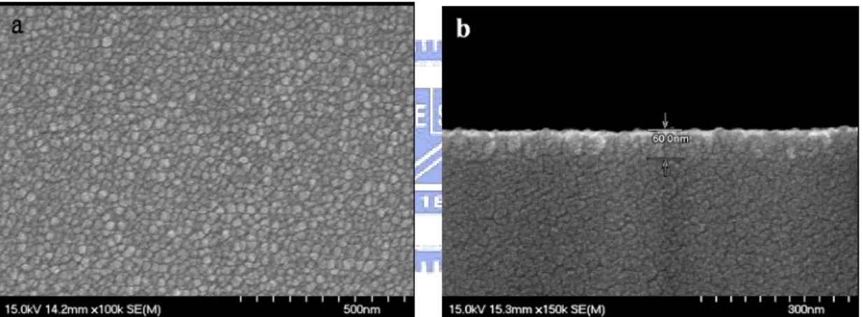
The epitaxial ZnO seeding layer was deposited by the RF-sputtering (30W at 1x10⁻² torr for 30 min at room temperature under Ar and O2 flowing rate
3:1). The thickness of the epitaxial ZnO seeding layer was about 60 nm. Figure 3-2 shows the top-view and cross-section SEM micrographs of the ZnO seeding layer grown on the Si substrate after annealing at 750℃ 3 hours under a keeping O2 flow rate of 30 sccm.
Figure 3-2. The SEM image of ZnO seeding layer on the Si substrate. (a) Top view (b) cross section.
3.1.2 The X-Ray Diffraction Analyses
Figure 3-3 shows the XRD patterns of ZnO seeding layer on Si substrate as deposition and after thermal annealing at 750℃ 3 hours under a keeping O2
flow rate of 30 sccm. It implied that the ZnO thin film has preferred orientation along (002) after annealing.
Figure 3-3. XRD patterns of ZnO seeding layer on Si substrate as deposition and after thermal annealing at 750℃ 3 hours.
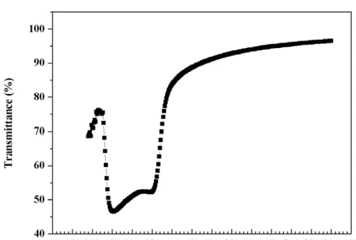
3.1.3 Ultraviolet-Visible Spectrophotometers Analyses
Figure 3-4show the transmittance spectra of ZnO seeding layer. It shows a low transmittance region at 250 nm-370 nm. It is because the energy band gap of ZnO is 3.37 eV. And at visible region, it shows a very high transmittance (>90 %).
3.2 ZnO Nanowires
The ZnO nanowires were synthesized by the hydrothermal method. The hydrothermal process has several advantages over other growth processes such as catalyst-free growth, low cost, large area uniform production, environmental friendliness, and low reaction temperature to integrate into the microelectronics. The source of the hydrothermal method was zinc nitrate hexahydrate (Zn(NO3)2.6H2O, (99.9%)) and hexamethylenetetramine (HMTA ; C6H12N4,
(99.9%)). The chemical solution was mixed with the ratio of 1:1. The Figure 3-5 was the pourbaix diagram for zinc. From the pourbaix diagram, if we want to form ZnO the pH value of the solution must control between 6 and 14. If the pH value of the solution was not between 6 and 14, there were many other compounds produced. The compounds included Zn2+(aq) , Zn(s) and
Zn(OH)42-(aq) . The pH value of the concentration from 0.01M to 0.5M before
growing is between 6 and 8 testing form the litmus paper. So in the experiment, it can grow ZnO nanowires. The pH value of the concentration after growing is lower than that before growing.
3.2.1
Characterization of ZnO Nanowires
The chemical solution concentration
The chemical solution concentration is a key factor of growing ZnO nanowires by the hydrothermal method. We changed the concentration from 0.5 M to 0.01M under the same growth time (3 hours) and same temperature (95℃). As raising the concentration of the chemical solution the ZnO nanowires become denser. When the concentration of the chemical solution was 0.5 M, the density of the ZnO nanowires was very high and it became a ZnO film. Beside, as decreasing the concentration of the chemical solution the diameter of the ZnO nanowires became smaller. The surface morphologies of the ZnO nanowires in different concentration of the chemical solution under the same growth time were shown in Figure 3-6. From the Figure 3-7,it is easy to observe that the aspect ratios of ZnO nanowires with different concentration of the chemical solution are different. Generally, the concentration of the chemical solution are higher the aspect ratios of ZnO nanowire are smaller. But the aspect ratio of ZnO nanowires grew at 0.01 M is lower than grew at 0.0125 M. It may be because that the source of 0.01 M is not enough for ZnO nanowires growing longer. So the aspect ratio is lower.
In order to fabricate the ZnO nanowires which have the better field emission characteristic or high surface area, we choose the concentration (0.0125 M) with highest aspect ratio of ZnO nanowires.
a b
c d
e
f
i
Figure 3-6. The SEM image ZnO nanowires grew in (a) 0.5 M (top view) (b) 0.5 M (cross section) (c) 0.1 M (top view) (d) 0.1 M (cross section) (e) 0.05 M (cross section) (f) 0.025 M (cross section) (g) 0.0125 M (top view) (h) 0.0125 M (cross section) (i) 0.01 M (cross section).
The growth time
The growth time of ZnO nanowires is another important parameter of hydrothermal method. In the experiment, we controlled the growth time from 30 min to 3 hours under the same concentration (0.0125M) of the chemical solution and keep in the same temperature (95℃). The morphologies of the ZnO nanowires with different growth time show in Figure 3-8. If the growth time is below 60min, there are no nanowires on the substrate. The dependence of the length of nanowires on growth time is illustrated in Figure 3-9. Observe from the Figure 3-9, there are two distinct growth kinetics: a very fast step, which takes from 60 min to 105 min with a growth rate of 43.99 nm/min and a relatively slow step with a growth rate of 2.70 nm/min, the fast step is about 16 times of the rate in the slow step.
Figure 3-10 show the XRD patterns of ZnO nanowires growing for 70 min and 120min. It implies that ZnO nanowires with growing 120 min had stronger peak of (002).
Figure 3-8. (a) Cross-section FE-SEM micrographs of ZnO nanowires at
0.0125 M with growing 60min (b) 75 min (c) 90 min (d) 105 min (e)120 min (f) 150 min (g) 180 min.
3.2.2
The Optical Properties
ZnO is a well-known semiconductor for its wide band gap and high exciton binding energy at room temperature. When the scale of system is under 100 nm, the new optical phenomenon may occur. So, it is important to understand the optical properties of the ZnO nanowires. Figure 3-11 shows the cathodluminescence (CL) spectra of ZnO nanowires with different growing time. The peaks of UV were both at about 374 nm (3.321eV). It is different with the ZnO band gap was 3.37 eV. It is because that the 3.321 eV was the band gap between the valence band and the excited state. The main peak of the visible light region is at about 575 nm (2.16 eV). By the figure 1-6, the deep-level emission is caused by the energy interval between the oxygen vacancies Vo level 766.9 nm (1.62 eV), single ionized oxygen vacancies VO*
level 540.24 nm (2.3eV) and oxygen interstitial Oi level 544.9 nm (2.28 eV).
The peak at 620 nm is the error of detector. The cathodluminescence (CL) mainly measured the UV signal from the valence band to the excited state.
Generally, there are two types of defects in the ZnO, one is the radiative defects and the other is nonradiative defects. The radiative defects were Vo, VO*, Zni, VZn, Oi and OZn. The nonradiative defects were the surface defects,
the lattice defects and etc.
When the ZnO nanowires formed by the hydrothermal method, the chemical component of the ZnO nanowires was nonstoichiometric, and usually consisted of excess Zn atoms and oxygen vacancies. Aftrer the ZnO nanowires formed, the surface of the ZnO nanowires was very unstable. It is easy to adsorb the steam and the impurities in the air to become the stable state on the surface of the ZnO nanowires. In other words, the steam and the impurities
formed the surface defects on the ZnO nanowires. These defects will make the UV intensity lower and luminescence higher.
From figure Figure 3-11, it can fine that the ZnO nanowires for 120 min had stronger UV peak and lower visible light region then the ZnO nanowire for 70 min. It means that the defects in the ZnO nanowires for 70 min are more than the defects in the ZnO nanowires for 120 min.
Figure 3-11. The CL spectra of ZnO nanowires for 70min and 120 min.
In order to decrease the defects of the ZnO nanowires, we put ZnO nanowires in the oven for thermal process. Figure 3-12 shows the
3.2.3 The Field Emission Properties
First, we show the Fowler-Nordhiem (F-N) function, which details were introduced at section 1-5. 3 2 2 2
exp[
]
J
β
β
Α Ε
ΒΦ
=
−
Φ
Ε
[3.1] 10 2 1.56 10 (− AV eV− ) Α = × [3.2] 3 3 26.83 10 (
eV V um
−)
Β =
×
[3.3] 3 2 2 2 1 ln( J ) ln( β ) β ΒΦ Α = − + Ε Ε Φ [3.4] 3 2m
β
ΒΦ
= −
[3.5]The J-E curves of ZnO nanowires on the Si substrate with different growth time are show in Figure 3-13. As show in figure, the ZnO nanowires with growth time 120 min had the better field emission property. The turn on field (Eon) defined as the electric field under the current density at 1.0 μA/cm2 and the threshold filed (Vth) defined as the electric field under the current density at 1.0 μA/cm2. The turn on voltage (Von) of ZnO nanowires with growth time 70 min, 90 min, 105 min, 120 min are 5 V/μm, 3.28 V/μm, 2.95
105 min, 120 min are 1039.8, 1464.25, 2082.1, 2475.8, respectively. The detail data of field emission property are showed in
Table 3-1.
It is well know that the β value depends on the geometry, structure, tip size and the number density of the emitters on the substrate. The ZnO nanowire with time 120 min had largest β. This phenomenon can be explained that a longer length of ZnO nanowires had better aspect ratio. It means that the point discharge effect is stronger, and consequently it provide the lowest turn on filed.
Figure 3-13. Field emission current-voltage curves of ZnO nanowires with different growth time.
70 min 90min 105 min 120 min Electrode Area 0.00709(cm2) 0.00709(cm2) 0.00709(cm2) 0.00709(cm2) Work
Function 5.37 eV (ZnO) 5.37 eV (ZnO) 5.37 eV (ZnO) 5.37 eV (ZnO) Eon 5 (V/μm) 3.28 (V/μm) 2.95 (V/μm) 2.75 (V/μm) Eth x 4.64 (V/μm) x x Slope of F-N plots 82.1 58.3 41 34.47 β 1039.8 1464.25 2082.1 2475.8 Average Length 649.25 (nm) 1291.3 (nm) 2157.5 (nm) 2173.3 (nm)
Table 3-1. The detail data of field emission property of ZnO nanowires with different growth time.
3.3 ZnO/TiO
2
Core-shell Nanowires
In order to fabricate the ZnO/TiO2 core-shell nanowires, the ZnO
nanowires must grew on the Si substrate by hydrothermal method first. The ZnO nanowires array had been fabricated, as show in the Figure 3-9.
Now we are focused on the TiO2 shell deposition process. The TiO2 shell
was deposited on ZnO nanowires by RF sputtering (13.56 MHz) under 5 mtorr Argon and Oxygen flow ratio 1:1 using TiO2 target at different sputtering
power, time and deposition temperature.
3.3.1 The Field Emission Scanning Electron Microscopy
Analyses
Figure 3-15& Figure 3-16 show the SEM micrographs of ZnO/TiO2 core-shell
nanowires. The ZnO nanowires which were used to fabricate the core-shell nanowires are 0.0125 M at 70 min and 120 min. Observe form Figure 3-15, it is easy to find that those core-shell nanowires are different to others. It is because that the TiO2 deposited at room temperature is not uniform. And others are
deposition at 150℃. In the other words, it means that higher deposition temperature can get uniform TiO2 thin film on the ZnO nanowires. It may be
reason is that the resolution of SEM is not enough. In the next section, we will discusse the ZnO/TiO2 nanowires by HR-TEM analyses.
a b
Figure 3-15. SEM images of ZnO/TiO2 core-shell nanowires deposited at room
a b
c d
e f
i
j
Figure 3-16. SEM images of ZnO/TiO2 core-shell nanowires with different
sputter arameters.
(a) ZnO nanowires grew 70 min and deposited TiO2 for 30w 30min at 150℃
(b) ZnO nanowires grew 120 min and deposited TiO2 for 30w 30min at 150℃
(c) ZnO nanowires grew 70 min and deposited TiO2 for 60w 30min at 150℃
(d) ZnO nanowires grew 120 min and deposited TiO2 for 60w 30min at 150℃
(e) ZnO nanowires grew 70 min and deposited TiO2 for 90w 30min at 150℃
(f) ZnO nanowires grew 120 min and deposited TiO2 for 90w 30min at 150℃
(g) ZnO nanowires grew 70 min and deposited TiO2 for 60w 60min at 150℃
(h) ZnO nanowires grew 120 min and deposited TiO2 for 60w 60min at 150℃
(i) ZnO nanowires grew 70 min and deposited TiO2 for 90w 90min at 150℃
3.3.2
The High Resolution Transmission Electron
Microscopy and Disersive X-Ray Energy Analyses
HR-TEM images and correspond selected area electron diffraction (SAED) pattern are showed in Figure 3-17, which illustrates the appearance and crystal structure of the ZnO/TiO2 core-shell nanowires. The ZnO nanowires grew for
70 min, and the TiO2 shell is deposition by sputter system with 90 W 90 min at
150℃. From Figure 3-17a, the structure had arc like tip. It is because TiO2 is
easier deposited on the tip center of ZnO nanowires. The diameter and length of this structure are 671.5 nm and 54.23 nm, respectively. Figure 3-17b-d are the images of region A, B and C, respectively. Form the Figure 3-17b, there is a TiO2 shell with 4.15 nm, 6.93 nm and 11.26 nm at right, left and top clearly.
From the Figure 3-17c, there is a TiO2 shell with 4.14 nm and 8.55 nm at right
and left side. Form the Figure 3-17d, there is a TiO2 shell with 4.32 nm at left
side. The thickness of TiO2 is not the same. It may be because the ZnO
nanowire did not stand on the substrate straightly. And it is found that ZnO nanowires grow along the [002] direction. The distance between parallel [002] is 2.6Å. The corresponding selected area electron diffraction (SAED) pattern of the core-shell structure is shown in Figure 3-17f. It shows that the ZnO
Figure 3-17. The TEM micrographs of (a) ZnO/TiO2 core-shell structure. (b)
region A (c) region B (d) region C. (e) The HR-TEM micrographs of region A (d) SAED spectra of region A.
Zn Ti O A 59.71% 10.03% 30.25% B 71.96% 1.49% 26.55% C 74.69% 1.41% 23.90% Table 3-2. The atomic percentage of ZnO/TiO2 core-shell structure analyses by
3.3.3
The X-Ray Diffraction Analyses
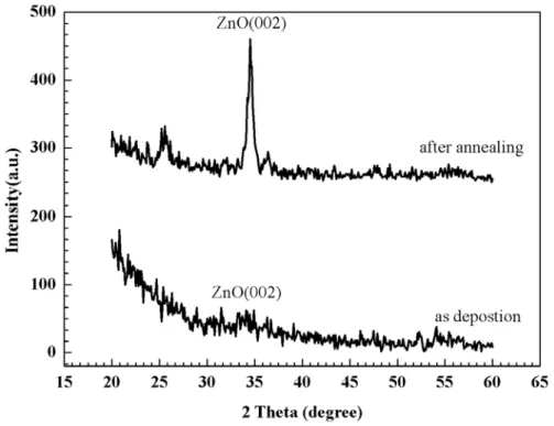
Figure 3-18a shows the XRD patterns of ZnO/TiO2 core-shell nanowires with
various sputtering power, time as TiO2 deposition. Figure 3-18b shows the
XRD patterns of the structure with various sputtering power, time after annealing 400℃ 1 hour in air. Figure 3-18c shows the XRD patterns of the structure with various sputtering power, time after annealing 500℃ 1 hour in air.
From Figure 3-18a, it only show the peak at ZnO(100), ZnO(101) and ZnO(002). It means that ZnO nanowires are wurtizite and no other phase appear and TiO2 shell on the ZnO nanowires is an amorphous type which are
consistent with TEM analyses. From Figure 3-18b-c, it still did not appear any TiO2 peak after annealing. Because of the lattice mismatch of wurtizite ZnO
between Rtile and Aatase TiO2, TiO2 is hard to form any crystal structure on
single crystalline ZnO nanowires. After the TiO2 deposition, the ZnO(002)
peak is somewhat a little shift form 34.300º to 34.502º.It means that the lattice constant of ZnO nanowres are changed. The small deviation of the lattice constants can be due to the lattice mismatch between TiO2 and ZnO.
Figure 3-18. The XRD patterns of ZnO/TiO2 core-shell structure with various
sputtering power, time (a) as TiO2 deposition, (b) after annealing 400 1 hour ℃
3.3.4
The Optical Properties
Figure 3-19 shows the the cathodeluminescence (CL) spectra of ZnO nanowires and ZnO/TiO2 core-shell structures as deposited. The ultraviolet
(UV) emission peak (374 nm) of ZnO is generally attributed to the exciton-related activity, and the visible light region (450-700 nm) may be due to the transitions of native defects such as Zn vacancies, Zn interstitials, oxygen interstitials and single ionized oxygen vacancies. The imperfect boundaries and stacking faults of ZnO nanowires would cause the unstable surface states to trap impurities and further damage the optical property. Figure 3-19 show that the UV peak of ZnO/TiO2 core-shell nanowires was stronger than the peak of
ZnO nanowires and the visible light region emission of ZnO/TiO2 core-shell
structures became very weaker. It may be because that coating an amorphous TiO2 film can repair the surface-related defects. Thus, the visible light region
emission decreased so that the UV emission become stronger. In conclusion, coating TiO2 film on ZnO is very important to improve the optical properties of
ZnO.
In order to get better optical characteristic of ZnO, we put the ZnO/TiO2
core-shell nanowires in the oven for thermal annealing 400 and 500 1 hour ℃ ℃ under the air. Figure 3-20 show the CL spectras of ZnO/TiO2 core-shell
visible light region emission may be because the nonstoichiometry TiO2
attracted the oxygen in the ZnO nanowires in the thermal process. It will produce many single ionized oxygen vacancies (VO*) in the ZnO nanowires.
Another reason is that after annealing Ti may diffuse into the ZnO nanowires. This phenomenon is resulted Zn vacancies (VZn), Zn interstitials (Zni), oxygen
interstitials (Oi) and single ionized oxygen vacancies (VO*) in the ZnO
nanwires. But the UV peak did not shift clearly and the ZnO(002) peak of XRD analyses is only a little shift. So that Ti may not diffuse into ZnO nanowires. Therefore, the main reason may be the nonstoichiometry TiO2. In conclusion,
ZnO/TiO2 core-shell nanowires as deposited had best optical property.
Figure 3-19. CL spectra of ZnO nanowires and ZnO/TiO2 core-shell nanowires
a
3.3.5
The Field Emission Properties
The field emission characteristics of ZnO/TiO2 core-shell nanowires are
indicated in Figure 3-22 and Table 3-3. Comparing with ZnO nanowries, ZnO/TiO2 core-shell nanowires had higher Eon and lower β value. In addition,
as the sputtered power and time increased, the turn on field increased. The reason may be that the nanowires with thicker TiO2 film had lower aspect ratio.
So that it is due to worse field emission properties. Another reason is that there is a barrier high at the interface between TiO2 and ZnO as show in the Figure
3-21. The inter fields will let surface electron toward ZnO. It will let electrons pass through hardly so that nanowires needed a higher electric field to emit the electron. This phenomenon will reduce the field emission current and lower the β value. In other word, this phenomenon is an advantage of ZnO/TiO2
core-shell nanowries which are used in DSSCs. The surface fields within each nanowire can be used to enforce charge separation and thereby ensure that faster transport results in a longer diffusion length in the nanowires.
Figure 3-21.Schematic energy level diagram of a ZnO/TiO2 core-shell
a
ZnO nanowires 60w 30min as deposition 90w 30min as deposition 60w 60min as deposition 90w 90min as deposition Electrode Area 0.00709(cm 2) 0.00709(cm2) 0.00709(cm2) 0.00709(cm2) 0.00709(cm2) Work Function 5.37 eV (ZnO) 4.5 eV (TiO2) 4.5 eV (TiO2) 4.5 eV (TiO2) 4.5 eV (TiO2) Eon 2.75 (V/μm) 3.01 (V/μm) 4.57 (V/μm) 4.59 (V/μm) 5.54 (V/μm) Eth x 4.86(V/μm) x 6.98(V/μm) x Slope of F-N plots 34.47 64 76 85 95 β 2475.8 1023 861.64 492.3696 689.31
Table 3-3. The detail data of field emission property of ZnO/TiO2 core-shell
nanowires as deposited.
The field emission characteristics of ZnO/TiO2 core-shell nanowires after
thermal treatment are indicated in Figure 3-23.The detail data of field emission properties of ZnO/TiO2 core-shell nanowires after annealing are indicated in
Table 3-4. As the figures showed, the turn on fields and the field enhance factor of different sputtering conditions became similar. So aspect ratio is not the critical reason at this case. It is know from the CL analyses that there are many defects in the ZnO nanowires after annealing such as VZn, Zni, Oi and VO* etc.
The defects will catch the electrons and holes. Therefore, there is a large recombination current in the ZnO nanowires. This current will reduce the field emission current and the decrease the β value. So after thermal treatment the field emission characteristics of ZnO/TiO2 core-shell nanowires are poorer.
a
60w 30min after anneal 500 1hour℃ 60w 60min after anneal 500 1hour℃ 90w 90min after anneal 500 1hour℃ Electrode Area 0.00709(cm2) 0.00709(cm2) 0.00709(cm2) Work Function 4.5 eV (TiO2) 4.5 eV (TiO2) 4.5 eV (TiO2) Eon 3.95 (V/μm) 3.90 (V/μm) 3.76 (V/μm) Eth 6.36(V/μm) 6.08(V/μm) 5.92(V/μm) Slope of F-N plots 80 76 75 β 818.56 861.64 873.13
Table 3-4. The detail data of field emission property of ZnO/TiO2 core-shell
3.4 TiO
2
Nanotubes
After the ZnO/TiO2 core-shell nanowires complete, we put the samples in
acetic acid (H2O:CH3COOH = 1000:1) for wet etching 30 min and 60 min.
After wet etching 60 min, the ZnO seeding layer is dissolved in the solution and then the ZnO/TiO2 core-shell nanowires float in the solution. So it is very
hard to observe. After wet etching 30 min the ZnO seeding layer is still exist and the nanowires are still on the substrate. At the following section we only discussed the ZnO/TiO2 core-shell nanowires after the wet etching 30 min.
3.4.1 The Field Emission Scanning Electron Microscopy
analyses
Figure 3-24a showed the top view ZnO/2 core-shell nanowires after the wet etching 30 min. There is a little different between after and before etching. After etching, some nanowires are lying on the substrate and some nanowires get together. They did not stand on the substrate straightly. It is because the seeding layer and some ZnO nanowires were etched by the acetic acid and there is no support in the TiO2 shell. Furthermore, when the sample is token out from the solution, the surface tension will bind nanowires together.
a
b
Figure 3-24. The SEM image of ZnO/TiO2 core-shell nanowires after wet etching 30 min (a) top view (b) cross section.
Microscopy Analyses and Disersive X-Ray Energy
Figure 3-25a showed the TEM image of TiO2 tube. Figure 3-25b showed
the high resolution image of the region B. The uniform diameter, length of the tube is 44.29 nm, 579.69 nm respectively. The TiO2 shell is 6.26 nm and 8.08
nm at right and left side. Figure 3-25c showed the SAED pattern of TiO2 tube.
It showed that there was no single crystalline structure in this tube clearly and the TiO2 was amorphous. The result is the same as the XRD. Table 3-5 showed
the composition of the tube which is analyzed by the EDX. It reveals that Zn (1.19 %) and Ti (98.81 %) at the top; Zn (3.61 %) and Ti (96.39 %) at the middle; Zn (6.83 %) and Ti (93.17 %) at the end. All the evidences indicated there is a hollow nanotube. In other words, the TiO2 can coat on the ZnO
nanowires at less 550 nm.
b
c
Figure 3-25. The TEM micrographs of (a) TiO2 tube. (b) region B (c) SAED
spectra of region B.
Zn Ti Region A 1.19 % 98.81 % Region B 3.61 % 96.39 % Region C 6.83 % 93.17 %
Table 3-5. The atomic percentage of ZnO/TiO2 core-shell structure analyses by
Figure 3-26a showed the TEM image of ZnO/TiO2 nanowires. Figure
3-26b showed high resolution image of region C. Form the Figure 3-26a, ZnO is still residual in the TiO2 shell after wet etching. The diameter and length of
this nanowire are about 54 nm and 651.5 nm, respectively. From the Figure 3-26b the TiO2 shell is about3.44 nm and 5.94 nm. Figure 3-27a-b showed the
SAED pattern of region B and C. It showed the there are ZnO nanowire and TiO2 shell at the region C. The ZnO nanowire is single crystalline with wurtzite
and TiO2 is amorphous type at region B. Figure 3-27 showed the TiO2 shell is
amorphous at the region C. Table 3-6 showed the atomic percentage of this nanowire. There are a large percentage of atomic at region A and region B. It impaled that there is ZnO under the TiO2 shell. In the other words, the ZnO
a
b
a
b
Figure 3-27. SAED spectra of (a) region B (b) region C.
Chapter 4
Conclusions
In summary, the hydrothermal method provides the simple, environmental friendliness, low cost and low temperature (below 100 ) way to grow ZnO ℃ nanowires. The ZnO/TiO2 core-shell nanowires and TiO2 tubes can be
fabricated by the sputtering method and simple wet etching process.
As the concentration of the chemical solution increases, the aspect ratio of ZnO nanowires decreased. As the growth time increases, the lengths of the ZnO nanowires increase.
After the TiO2 coating on the ZnO nanowires the optical properties were
improved. The UV emission became very strong and visible emission became very weak. After the thermal treatment, the UV emission became very weaker and visible emission became very stronger. It may because of the nonstoichiometry TiO2 attract the oxygen from the ZnO nanowires during the
thermal process. The phenomenon produced many single ionic oxygen vacancies in the ZnO nanowires and impaired the optical properties.
After TiO2 coating, the field emission characteristic will change. The turn
on filed increased and the β value decreased. It may because that the nanwires with thicker TiO2 film has lower aspect ratio. Another reason is that there is a
barrier high at the interface between TiO2 and ZnO. The inter field will let the
electron pass through hardly and nanowires needed a higher electric field to emission. After the thermal treatment, there will be many defects in the ZnO. And the defect will catch the electron and become a recombination current in the ZnO nanowires so that it reduced the field emission current.
dye-sensitized solar cells. The surface fields within each nanowire can be used to enforce charge separation and thereby ensure that faster transport results in a longer diffusion length in the nanowires.
Reference
1 Q. B.Wu, S. Ren, S. Z. Deng, J. Chen, and N. S. Xu J. Vac. Sci. Technol.
B22(3),1282 (2004).
2 P. L. Chen, J. K. Chang, C. T. Kau, and F. M. Pan, Appl. Phys. Lett 86,
123111 (2005).
3 K. H. Jung, J. W. Yoon, N. Koshizaki and Y. S. Kwon Jpn. J.Appl. Phys. 44,
7A 5300 (2005).
4 S. H. Jeong and K. H. Lee Jpn. J. Appl. Phys 8B, L1106 (2004).
5 H. O. Le and S. J. Chua, Y. W. Koh and K. P. Loh, Z. Chen, C. V. Thompson
and E.A. Fitzgerald Appl. Phys. Lett 87, 101908 (2005).
6 Y. F. Mei, Z. M. Li, R. M. Chu, and Z. K. Tang, G. G. Siu, Ricky K. Y. Fu,
and Paul K. Chu, W. W. Wu and K. W. Cheah Appl. Phys. Lett 86, 021111 (2005).
7 Y. B. Tang, H. T. Cong, Z.G. Zhao, and H. M. Cheng Appl. Phys. Lett 86,
153104 (2005).
8 H. Hu, K. Yu, J. Zhu, Z. Zhu. Applied Surface Science 252, 8410–8413
(2006).
9 B. Cao, W. Cai, Y. Li, F. Sun and L. Zhang, Nanotechnology 16, 1734
(2005).
10 C. L. Kuo, T. J. Kuo, and M. H. Huang J. Appl. Chem. B 109,20115
(2005).
11 F. Xu, K. Yu, G. Li, Q. Li and Z. Zhu, Nanotechnology 17, 2855–2859
(2006).
12 M. H. Liao, C. H. Hsu, D. H. Chen, Journal of Solid State Chemistry 179,


![HPSH [ 氧化數平衡反應式係數 ]](data:image/gif;base64,R0lGODlhAQABAIAAAP///wAAACH5BAEAAAAALAAAAAABAAEAAAICRAEAOw==)