國 立 交 通 大 學
電子工程學系 電子研究所碩士班
碩 士 論 文
二氧化鉿電阻式記憶體
多位元操作之隨機電報雜訊分析
The Random Telegraph Noise (RTN) Analysis of
Multi-Level Operation Methods in HfO
2-based Resistive
Random Access Memory
研 究 生 :黃英傑
二氧化鉿電阻式記憶體多位元操作之
隨機電報雜訊分析
The Random Telegraph Noise (RTN) Analysis of
Multi-Level Operation Methods in HfO
2-based Resistive
Random Access Memory
研 究 生 : 黃英傑 Student : Ying-Jie Huang
指導教授 : 莊紹勳 博士 Advisor : Dr. Steve S. Chung
國立交通大學
電子工程學系 電子研究所碩士班
碩士論文
A Thesis
Submitted to Department of Electronics Engineering and
Institute of Electronics
College of Electrical and Computer Engineering
National Chiao Tung University
In Partial Fulfillment of the Requirements
for the Degree of
Master of Science
in
Electronics Engineering
二氧化鉿電阻式記憶體
多位元操作之隨機電報雜訊分析
研究生:黃英傑 指導教授:莊紹勳博士
國立交通大學電子工程學系電子研究所碩士班
摘要
電阻式記憶體近年來成為非揮發性記憶體的熱門探討主題,歸因於
其擁有面積小、高密度、低成本以及低耗能等優勢。在眾多材料當中,
以二氧化鉿為基底的電阻式記憶體和現今的高介電係數電晶體製程技術
最為相容,也較成熟。電阻式記憶體儲存狀態的方法是透過不同電壓條
件改變阻態,不少文獻指出此變化歸因於二氧化鉿絕緣層於不同偏壓下
所產生的軟性崩潰(soft breakdown)所致。
然而為了提高儲存密度,一方面在單一元件中必須設法達到多位元
的存取,另一方面必須確保各狀態判讀不能有誤,精準控制每個狀態是
必要的。隨著元件面積持續縮小,在氧化層中單一缺陷對電流反映出的
影響所占比重增加,因此隨機電報雜訊(random telegraph noise)所帶來的
問題不容小覷,它將嚴重的影響我們元件中各狀態判讀的正確與否。隨
機電報雜訊分析可被用來詳細探討高介電係數電晶體之載子行為。
式在單一元件中來達成多位元的存取並分別探討其可靠度問題,包含寫
入狀態的資料保存、多次重覆寫入/抹除的元件耐久性、面積對重覆寫入
/抹除的阻值不穩定關係等。我們運用隨機電報雜訊分析,來分析路徑產
生對記憶體的判讀產生的影響。藉由分析捕捉時間(capture time)與發射時
間(emission time),吾人可以計算出缺陷位置、能量的深度;並運用隨機
電報雜訊電流擾動的振幅,對應比較不同的操作方法,幫助吾人分析不
同增壓速率下其軟性崩潰路徑的分佈。實驗結果顯示,電壓增加速率的
快慢關係著元件氧化層中軟性崩潰路徑的分散與集中;軟性崩潰路徑越
分散,則元件轉態後阻值將越不穩定,影響判讀準位。
The Random Telegraph Noise (RTN) Analysis of
Multi-Level Operation Methods in HfO
2-based Resistive
Random Access Memory
Student:Ying-Jie Huang Advisor:Dr. Steve S. Chun
g
Department of Electrical Engineering & Institute of Electronics
National Chiao Tung University
ABSTRACT
Resistance-change Random Access Memory (RRAM) has recently received much more attention owing to its potential layout toward high-density, low-cost, and low-energy non-volatile memory. More recently, the dielectric HfO2 has become the mainstream of
modern transistor and capacitor microelectronics, and is now a strong candidate for RRAM applications. The switching mechanism of HfOx RRAM has been considered as the
formation and rupture under applied bias of the soft-breakdown paths. To achieve large bit storage in a scaled device with a high density memory cell array, multi-level operation is required. To achieve this requirement and maintain a large resistance memory window, both the low resistance state and high resistance state must be significantly controlled. One of the important phenomena, the current fluctuation caused by the Random Telegraph Noise (RTN) has created a huge impact on the read-out of the RRAM, in particular for multi-level applications. RTN analysis is extensively used to study electron transport in
In this work, we have studied the effect of sweep and pulse operations for the RRAM device to achieve multi-level storage. The multilevel storage characteristics of our study showing that different resistance states of the RRAM device can be achieved by different operation voltages or currents. We discussed the reliability issues including data retention time, program/erase cycling endurance, and the cell size dependence of the resistance fluctuation.
The RTN signals have been utilized to examine the effects of soft breakdown paths status in RRAM devices. By observing the bias and temperature dependence of capture and emission time, the defect location could be identified. Through both post-sweep and post-pulse RTN current measurements, we found a different trend of the RTN current amplitude between these two operation methods. Results show that the voltage ramping rate during the forming and set process (transition from the high resistance to the low resistance state) is a key parameter to determine the distribution of soft breakdown paths. The dispersed one will cause the instability of switched resistance, and induce the erratic bit during the read-out of RRAM.
誌 謝
兩年的實驗室生活是精采豐富的,但同時也充滿嚴苛的挑戰。首先
感謝的是我的指導老師:莊紹勳教授,在學術專業上的指導與建議,開
啟了我對未知領域的大門,無私的付出默默的關懷,讓我在學業上與研
究上獲益良多。處事態度方面也使我增長不少,對事物應必須有的嚴謹
態度以及處理方法,無時無刻都得戰戰兢兢面對所有挑戰,故我必須在
此表達感謝之意。
感謝已畢業的元宏、承翰學長,當我在實驗遇到瓶頸和挫折時,總
是能適時給予指導,並提供我想法。也感謝在兩年研究生涯中,與我一
起同甘共苦的同學們,包括漢旻、政達與侑璉,我們一起經歷困苦的研
究過程,相信數年後再聚首,一定倍感溫馨;除此之外還有一群天真活
潑的學弟們,包括敬翰、邦齊、尚墩、宗慶、漢樽,我會懷念和你們聊
天打屁一起打球的日子,輕遞一份祝福,希望明年亦能看見你們順利的
畢業。對於汪老師研究群的同學,雖然我們身在不同的研究群,但我們
的感情就像是一家人一樣,特別感謝榮標學長、泓達、定樺,有了你們
陪伴,讓我感到實驗室變得繽紛許多。
最後我要感謝我的家人們,你們是我最大的精神支柱,有了你們的
支持與鼓勵,讓我可以不畏艱難的向前邁進。
謹將這份榮耀獻給培育我多年的父母親。
Contents
Chinese Abstract --- i
English Abstract --- iii
Acknowledgements --- v
Contents --- vi
Figure Captions --- viii
Chapter 1 Introduction……….……….….…
1
1.1 Background………...………..…………... 1
1.2 The Motivation of this Work………...………... 2
1.3 Organization of the Thesis……….. 3
Chapter 2 Device Preparation, Equipment Setup, and Measurement Methods….…. 4
2.1 Device Preparation………...………….………. 42.2 Equipment Setup……….………..……….……...………. 4
2.3 Measurement Methods…………..………...………...………. 5
Chapter 3 Multi-Level Storage and Reliability Issues of RRAM…………..……… 19
3.1 Introduction……….…... 19
3.2 The Sweep Operation of RRAM ……….………..……...…. 19
3.2.1 The Switching Parameter Definitions of RRAM……….…………... 19
3.2.2 Compliance Current……….…..……...………....…………... 20
3.2.3 SET Operation by Different Compliance Currents…..……...……... 20
3.2.4 RESET Operation by Different Stop Voltages……..…..……... 20
3.2.5 Discussion………..…...…..……...……... 21
3.3 The Pulse Operation of RRAM ………..………….………...…………. 22
3.3.1 SET Operation by Different Pulse Amplitudes...……….……...……...…... 22
4.2 General Equation of RTN………...……… 40
4.2.1 Capture and Emission Time………...…... 40
4.2.2 Trap Depth………..……….. 41
4.2.3 Trap Energy………...……… 42
4.3 RTN Phenomena After the Sweep Operation………..………...…..…………. 43
4.3.1 RTN Measurement………...………. 43
4.3.2 Capture and Emission Time………...……... 44
4.3.3 Trap Depth………..……….. 44
4.3.4 Trap Energy………...……… 45
4.4 RTN Phenomena After the Pulse Operation………...………..…... 45
4.4.1 RTN Measurement………...………. 45
4.4.2 Capture and Emission Time………...…... 46
4.4.3 Trap Depth………..……….. 46
4.5 Noise Amplitude………..……….. 46
4.5.1 Noise Amplitude Measurement………..……….. 46
4.5.2 Discussion………...……….. 47
Chapter 5 Summary and Conclusion….………...………... 64
Figure Captions
Chapter 2
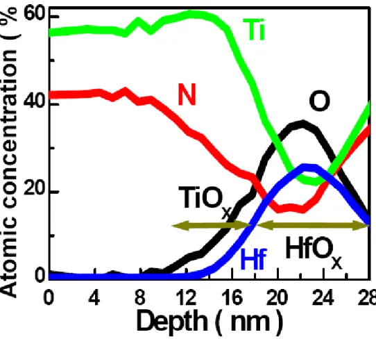
Fig. 2.1 XPS depth profile of TiN/Ti/HfO2/TiN stack layers after alloying. 9
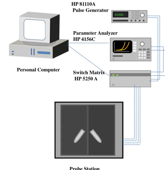
Fig. 2.2 The experimental setup of the current-voltage and the P/E cycling endurance
characteristics measurement in RRAM. Automatic controlled characterizations system is setup based on the PC controlled instrument environment.
10
Fig. 2.3 The cross section of transition metal oxide based resistive switching memory
during forming process.
11
Fig. 2.4 Forming: the predominant step before resistive switching operation. 12
Fig. 2.5 Two terminologies of RRAM. (a) unipolar and (b) bipolar. 13
Fig. 2.6 Basic characteristics of the test RRAM cells in this thesis. 14
Fig. 2.7 Illustration of positive sweep operation in RRAM. 15
Fig. 2.8 Illustration of negative sweep operation in RRAM. 16
Fig. 2.9 The timing diagram of the triggered pattern mode method during (a) program
and (b) erase operations.
17
Fig. 2.10 Illustration of sampling operation. 18
Chapter 3
Fig. 3.1 Typical current-voltage characteristics of RRAM. C.C. denotes the compliance
current. Vstop denoted the maximum negative sweep voltage. Vreset or Ireset,max are the voltage or current at which reset takes place. Vset is the voltage at which set takes place.
26
Fig. 3.5 Ireset, max during sweep is at the same current order as the previous set process. 30
Fig. 3.6 Illustration for the semi-on state. (a) The state we pick off which is not
conducted enough. (b) The current is dominant by tunneling component since the soft breakdown generating paths are not complete.
31
Fig. 3.7 Data retention properties of various states by sweep operation. The result
predicts 10 years lifetime of each state.
32
Fig. 3.8 The program/erase cycling endurance characteristics of sweep operation. L1
and L2 are the LRS with 650 µA and 200 µA compliance currents respectively. L3 and L4 are the HRS where the stop voltages are -1.0 V and -1.5 V.
33
Fig. 3.9 The pulse voltage dependence of the resistance at low resistance state in
TiN/TiOx/HfOx/TiN device. The positive pulse width is 1x10⁻⁸ sec.
34
Fig. 3.10 The pulse width dependence of the resistance at high resistance state in
TiN/TiOx/HfOx/TiN device. The negative pulse amplitude is -2 V.
35
Fig. 3.11 Data retention properties of various states by pulse operation. The result
predicts 10 years lifetime of each LRS, but not HRS.
36
Fig. 3.12 (a) The high resistance states overlap after 10 sec. (b) By sensing the current,
the random telegraph noise (RTN) phenomena is observed. The ∆I/I is larger than 30 %.
37
Fig. 3.13 The program/erase cycling endurance characteristics of pulse operation. The
resistance fluctuation is serious after each switching.
38
Fig. 3.14 Cell size dependence of the resistance variation (∆Rmax/R) in 1000 times
set/reset cycles.
39
Chapter 4
Fig. 4.1 The schematic plot of current instability due to electrons trapped. (a) Trap
empty state, (b) Trap filled state.
Fig. 4.3 Current waveform of RRAM device which is operation by sweeping method
(S1), C.C. = 500 µA, Vstop = -1.5 V.
51
Fig. 4.4 Current waveform of the other RRAM device which is operation by sweeping
method (S2), C.C. = 500 µA, Vstop = -1.5 V, after 20 times set/reset cycles.
52
Fig. 4.5 Variation of capture time τc and emission time τe as top voltage increases. (a) S1 and (b) S2.
53
Fig. 4.6 Relationship between τc/τe and top voltage. The extracted ZT from the slope is 1.86 nm and 3.35 nm for S1 and S2 from top electrode respectively.
54
Fig. 4.7 eT2 versus 1/kT plots for S1. Energy difference between conduction band of dielectric and trap (Ec-ET) is around 0.68 eV. (a) Vtop = 0.06 V, (b) Vtop = 0.16
V, and (c) Vtop = 0.26 V.
55
Fig. 4.8 τeT2 versus 1/kT plots for S1. Energy difference between conduction band of dielectric and trap (Ec-ET) is around 0.77 eV. (a) Vtop = -0.06 V, (b) Vtop =
-0.16 V, and (c) Vtop = -0.26 V.
56
Fig. 4.9 Current waveform of RRAM device which is operated by pulse method (P1),
forming process with 4 V pulse amplitude and 1.6x10⁻⁶ sec pulse width, reset by a negative pulse with -2 V amplitude and 1x10⁻⁶ sec pulse width.
57
Fig. 4.10 Current waveform of RRAM device which is operated by pulse method (P2),
forming process with 4 V pulse amplitude and 9x10⁻⁷ sec pulse width, reset by a negative pulse with -2 V amplitude and 1x10⁻⁶ sec pulse width.
58
Fig. 4.11 Variation of capture time τc and emission time τe as top voltage increases. (a) P1 and (b) P2.
59
Fig. 4.12 Capture time to emission time ratio versus gate voltage plots. (a) P1, (b) P2.
The extracted ZT from the slope is 4.46 nm and 2.86 nm for P1 and P2 from 60
(a) Magnitude of current plot, (b) ∆I vs. Vtop and, (c) ∆I/I vs. Vtop.
Fig. 4.15 Illustration for the soft breakdown paths distribution after different operation
methods. (a) Sweep operation. (b) Pulse operation.
Chapter 1
Introduction
1.1 Background
Today, silicon-based flash memory has become the most promising nonvolatile memory because their high density, yield, and the compatibility with current CMOS technology. However, flash memory now faces an inevitable scaling problem limited by the tunnel oxide thickness [1.1]. To solve this issue, nitride storage flash, usually called SONOS, has been developed [1.2]. Although SONOS may continue the scaling of tunnel oxide thickness, several inherent problems of these charge-trapping type nonvolatile memories emerges, such as random dopant fluctuation [1.3], random telegraph noise [1.4], stress induced leakage current [1.5], and trap-assist tunneling [1.6], etc. Next generation nonvolatile memory has a possibility to replace the charge-trapping storage by the dielectric resistance change. Among these, there are four main categories of the emerging memories: Ferroelectric RAM (FeRAM), Magnetoresistive RAM (MRAM), Phase Change Memory (PCM), and Resistive RAM (RRAM). FeRAM exhibits lowest power, while MRAM shows fastest switching. PCM and RRAM have moderate power consumption and switching rate but exhibit scaling potential, which makes them more attractive [1.7, 1.8]. Nevertheless, the self heating of PCM poses great challenges due to frequent high temperature re-crystallization. As a consequence, RRAM becomes the most popular
1.2 The Motivation of This Work
About forty years ago, several papers reported that chalcogenide material sandwiched between two metal electrodes may change its conductivity under applied electric field [1.9-1.10]. This discovery did not attract much attention because nonvolatile memory was not popular at that time and the device scaling was not a critical issue. Not until the report of electric-pulse-induced reversible resistance change made by S. Q. Liu in 2000 [1.11], this resistive random access memory draws more interests as a potential candidate which is a strong candidate for the next generation nonvolatile memory.
Many materials have been considered as potential candidates of the dielectric for RRAM. In general, we may classify these materials into three categories: (1) Perovskite, (2) Transition Metal Oxide, and (3) Organic and Macromolecule materials. The perovskite material, such as Pr0.7Ca0.3MnO3 (PCMO) and La0.7Ca0.3MnO3 (LCMO), was first
developed owing to its close connection with FeRAM [1.12-1.14]. The organic materials attract lots of interests in recent years because of their potential applications [1.15]. However, the transition metal oxide based RRAM shows best performance, reliability, and conventional fabrication compatibility. There have been numerous reports on transition metal oxide materials, such as SrTiO3, TiO2, ZrO2, NiO, TaO2, HfO2, WO2, etc
[1.16-1.22]. Some reports also mentioned the importance of electrode material, which may
determine the existence of RRAM switching behavior using the same insulator [1.23].
Besides a variety of dielectric materials, the switching mechanism of RRAM also raised controversies, such as Mott transition, Jahn-Teller Effect, and ionic dopant drift, etc
manifested that there is one or several conduction filaments connecting between two electrodes, and the formation and rupture of the filaments control the measured resistance
[1.25].
To achieve large bit storage in a scaled device with a high density memory cell array, multi-level operation is required. By using different operation methods, the memory devices may endure different damage and show different characteristics. In this thesis, we use hafnium oxide as RRAM dielectric to investigate the operation methods of transition metal oxide based RRAM. We achieved the multi-level storage, and discuss the effect by using different operation schemes.
As the device dimensions continue to shrink with each generation, the effect of each defect on device becomes more pronounced. The current fluctuation due to Random Telegraph Noise (RTN) resulted in errors in the read-out with multi-level operation. In this thesis, we will also use the current fluctuation of RTN to investigate and compare the difference between different operating schemes.
1.3 Organization of the Thesis
There are five parts in this thesis. Chapter 1 is the introduction. We describe the motivation and organization of this thesis. In Chapter 2, we show the device preparation and equipment setup used in the experiments. In Chapter 3, we will examine the methods
Chapter 2
Device Preparation, Equipment Setup, and
Measurement Methods
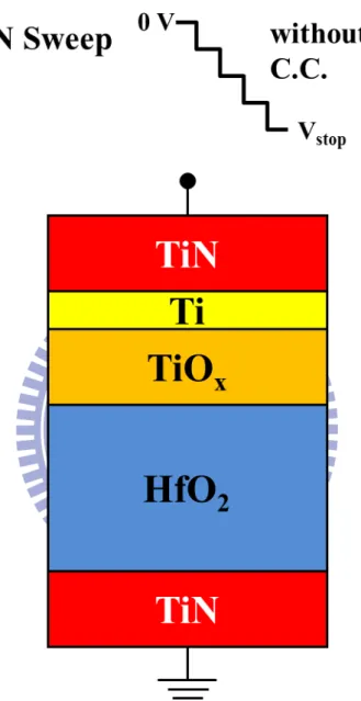
2.1 Device Preparation
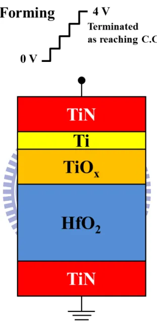
The structure of RRAM is the TiN / TiOx / HfOx / TiN stack, which was deposited
on the Ti / SiO2 / Si substrate. The HfO2 thin film was deposited by atomic layer
deposition (ALD), while all the other thin films were deposited by sputtering methods. Owing to the well-known ability of Ti to absorb oxygen atom [2.1], oxygen atoms diffuse from the HfO2 layer to the Ti, resulting in the formation of HfOx (x ~ 1.4) with a large
amount of oxygen deficiency and the oxidation of Ti. The corresponding XTEM image, made by the XPS examination, is presented in Fig. 2.1 [2.2].
2.2 Equipment Setup
The whole experimental setup for the I-V and pulse characteristics measurement of RRAM is illustrated in Fig. 2.2. Based on the PC controlled instrument environment by HP-IB (GP-IB, IEEE-488 Standard) interface, the complicated and long-term characterization procedures to analyze the behaviors in RRAM cells can be easily achieved. As shown in Fig. 2.2, the equipment, including the semiconductor parameter analyzer (Agilent 4156C), low leakage switch mainframe (HP 5250A Switching Matrix), pulse
devices. Programs written by HT-Basic were used to execute the measurement via HP-IB interface.
The Agilent 4156C provides a high current resolution up to pico-ampere range, and is equipped with four programmable source/monitor units. Two source units, and two monitor units for supplying or monitoring the voltage and the current. The pulse generator Agilent 81110A with high timing resolution provides for P/E cycling endurance. The HP 5250A switching matrix equipped with an 8-input x 12-output switching matrix switches the signals from the Agilent 4156C and Agilent 81110A to device under test in the probe station automatically.
2.3 Measurement Methods
2.3.1 Introduction
There are four measurement techniques used in this thesis. First, a forming process is required for every fresh device before normal operation. Second, normal operation using bipolar voltage sweep is necessary for basic device characterization. Third, the pulse with both positive and negative pulses causes the changes of RRAM devices to high/low resistance state. The last one is the sampling mode which helps us to read the RRAM devices resistance and sensing the Random Telegraph Noise (RTN) signal.
Before we start to operate the RRAM correctly, performing the so-called “forming” procedure in the beginning is required, as shown in Fig. 2.3. We add a ramping voltage on the top TiN electrode which is near the Ti buffer layer, and measure the corresponding current by Agilent 4156C semiconductor parameter analyzer. When the accumulated energy exceeds a certain limit determined by the device material and thickness [2.3], the current reaches at the value of compliance current, and the forming step is accomplished, as shown in Fig. 2.4. The compliance current is usually set to be a little less than the compliance used in normal SET process.
2.3.3 Sweep Operation
After the “forming” process, this device switches to LRS (Low Resistance State). The following step is to turn it off, i.e., to switch the RRAM from LRS to HRS (High Resistance State). There are two operation modes to identify the switching type of RRAM devices [2.4]. As shown in Fig. 2.5, one is unipolar, and the other one is bipolar. Unipolar means that the turn on voltage and turn off voltage are at the same polarity, where the turn on voltage is usually larger than turn off voltage. On the other hand, the bi-polar means that the turn on voltage and turn off voltage are in opposite polarities. Usually the bi-polar switching device is more suitable for future CMOS technology owing to less operation voltage and power consumption. The basic characteristic of a typical device is shown in
Fig. 2.6, which is obviously a bipolar device. The illustrations of voltage sweep operations
in this work are shown in Fig. 2.7 and Fig. 2.8.
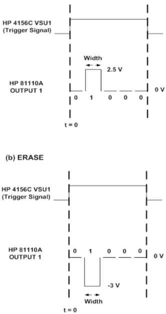
In order to control the pulse timing of Agilent 81110A during transient and P/E cycling endurance characteristics precisely, we select the triggered pattern mode to achieve this goal. Fig. 2.9 (a) and Fig. 2.9 (b) show the program and erase schemes on the RRAM devices respectively. For example, by taking the programming timing pattern as shown in
Fig. 2.9, the triggered pattern mode can be explained as follows. In Fig. 2.9 (a), the VSU1
of Agilent 4156C generated a voltage signal which is equal to the low voltage level of Agilent 81110A. This triggered pattern mode method can provide a substrate bias during programming, and prevent additional stress to device during P/E cycling endurance operation. The pattern mode defined as 01000 in Fig. 2.9 (a) from Agilent 81110A is then sent and the program or erase operation is performed.
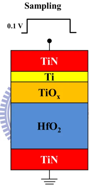
2.3.5 Sampling
After the sweep and the pulse operation, we have to check whether the RRAM device is switched successfully. So, we have to sense the currents by Agilent 4156C under a read voltage for a period of time and then average them to get the resistance. Fig. 2.10
illustrates the concept of this measurement method. This sampling procedure reads RRAM by applying 0.1 V to evaluate current and resistance. The 0.1 V is chosen to be less than RRAM switching threshold to avoid disturbance.
The Random Telegraph Noise (RTN) signal is extracted by the same method; we can say that is the long time read operation. RRAM current is about 100 nA ~ 100 µA. The
2.3.6 Statistics of Random Telegraph Noise
The target of RTN measurement is to extract mean capture and emission time and then further profile traps properties. Therefore, the switching of trap captures and electrons emitting must be distinguished. We can determine using naked eye and it’s also the most precise method to obtain mean capture and emission time. Nevertheless it wastes time and not efficient for large amount of data. In our work, we wrote a program and used a current level that lies in the middle of the high and low current state to differentiate trap holding or releasing an electron automatically. Sequentially, every period of time was added and divided by numbers of events. As a consequence, we extracted more accurate mean capture and emission time which can handle much larger amount of data.
01000 Probe Station Personal Computer HP 81110A Pulse Generator Parameter Analyzer HP 4156C Switch Matrix HP 5250 A
Fig. 2.2 The experimental setup of the current-voltage and the P/E cycling endurance
characteristics measurement in RRAM. Automatic controlled
characterization system is setup based on the PC controlled instrument environment.
Fig. 2.3 The cross section of transition metal oxide based resistive switching memory
(a)
(b)
Fig. 2.9 The timing diagram of the triggered pattern mode method during (a)
Chapter 3
Multi-Level Storage and Reliability Issues of RRAM
3.1 Introduction
In this chapter, we will show the operation methods of resistive random access memory to achieve multi-level storage and the associated definitions. One method is sweep operation, the other one is pulse operation. Also, we will discuss the reliability issues after different operating methods. Regarding the reliability, we measure the resistance loss at 100 oC after these operations, to observe the data retention characteristic of these devices. After that, we will compare the program/erase cycling endurance between sweep and pulse operation methods. From different operation methods, we discuss the advantages and shortcomings for distinct use of the device.
3.2 The Sweep Operation of RRAM
3.2.1 The Switching Parameter Definitions of RRAM
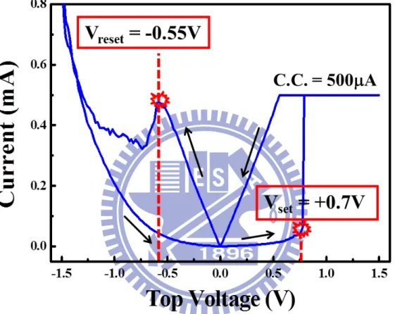
The main parameters used in this thesis are shown in Fig. 3.1. When RRAM is switched to LRS, we define Vset as the turn on voltage, and Iset as the corresponding
we define the maximum negative voltage as Vstop.
3.2.2 Compliance Current
The objective for setting the compliance current is to prevent the dielectric hard breakdown of the RRAM device [3.1]. During the “forming operation” and the “set operation,” we must have to set the compliance current to ensure not to destroy the function of the RRAM device. In this case, the compliance current is achieved by Agilent 4156C via the HT-BASIC language.
3.2.3 SET Operation by Different Compliance Currents
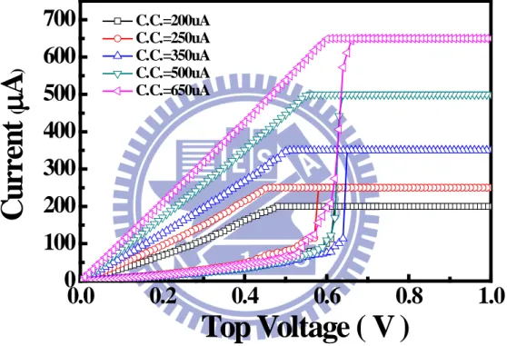
As shown in Fig. 3.2, for the low resistance state (LRS), we can achieve multi-level storage by using different compliance currents. When the top voltage ramped up, the soft breakdown paths were generated. The voltage step is set very small to ensure that these soft breakdown paths are formed slowly and concentrated [3.2]. Then, we setup the compliance current during the positive sweep; the compliance current level will be able to control these soft breakdown paths’ number or cross-section. When the RRAM current reaches the compliance current that we set, this current will be fixed by Agilent 4156C. In other words, the soft breakdown paths stop growing. Different sizes of soft breakdown paths correspond to different RRAM resistances. In the meantime, the soft breakdown paths’ size increased, the current increased under same read voltage. So, we can achieve multi-level storage in the low resistance state by changing different compliance currents.
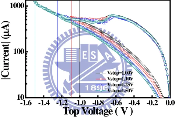
For the high resistance state (HRS), RRAM device after a negative voltage sweep now changes the resistance state. During this process, some soft breakdown paths are rupture which can be caused by reoxidation of a narrow filament tip adjacent to the electrode [3.3]. So the number of these conductive paths is decreased obviously. All of these soft breakdown paths will be eliminated when the absolute value of the stop voltage is large enough. In other words, the RRAM current must be a tunneling current because the soft breakdown paths are separated from the electrode [3.4]. Also as mentioned above, the multi-level storage can be achieved by changing different stop voltage Vstop, which is
shown in Fig. 3.3. The absolute value of stop voltage increases, the RRAM resistance increases as well, as shown in Fig. 3.4.
3.2.5 Discussion
The current is a key performance metric for the operation of RRAM devices as it governs the power needed for switching operation [3.5]. For the low power operation of the memory devices, we should reduce reset current. As shown in Fig. 3.5, RESET current (Ireset) and set current (compliance current) are interrelated. The order of these two currents
is the same. So, we can lower the compliance current of forming and set process to achieve a low power operation.
When the RRAM device is switched to low resistance state, i.e., set process, if the compliance current we setup is too small, the soft breakdown paths are not completely
compliance current level, i.e., the maximal resistance at low resistance state (LRS).
For the data retention characteristics, we achieve the different resistance levels by the sweep operation. The LRS data writing for five resistance levels has been demonstrated by varying the compliance currents of sweep process. In Fig. 3.7, the LRS multi-level resistance is achieved by five compliance currents (200 µA ~ 650 µA) at 100 o
C, and we check the prediction of the retention time for 10 years. Furthermore, the HRS multi-level storage is achieved by different stop voltages. We vary four different stop voltages (-1.0 V ~ -1.5 V), and it shows good data retention characteristics. Here, we can obtain nine different levels on one cell, while it still maintains distinct levels after 10,000 seconds.
The program/erase cycling endurance characteristics of sweep operation are shown in Fig. 3.8. L1 and L2 are the LRS with 650 µA and 200 µA compliance currents respectively. L3 and L4 are the HRS where the stop voltages are -1.0 V and -1.5 V. We can see that the resistance fluctuation is larger. The larger resistance state shows larger resistance variation. For the purpose of the data retention use, we can control the device with nine levels and even more. But if we consider this device for cycling endurance objective, the level number should be reduced. Otherwise, the neighboring states will be overlapped. It will result in errors in the read-out during multi-level operation.
3.3 The Pulse Operation of RRAM
RRAM device. The same as sweep operation, we add a positive bias to RRAM top electrode to accomplish the set process. There are some differences between these two operation methods. First, the voltage changing rate from 0 V to Vhigh of pulse is larger than
the sweep operation. Second, the pulse voltage (Vhigh) is always higher than the turn on
voltage of the sweep operation.
The multi-level operation is achieved by changing the pulse amplitudes. The pulse width is 1x10⁻⁸ sec, by changing the pulse amplitudes from 1.5 V to 2.5 V. Then, we will get different resistance levels, as shown in Fig. 3.9. The resistance decreases as the pulse voltage increases. So, the RRAM resistances at the low resistance state can be controlled by different pulse voltages to achieve multi-level storage.
3.3.2 RESET Operation by Different Pulse Widths
Different from the set operation, to achieve multi-level storage of high resistance state (HRS), we control the width of the negative pulse. The pulse amplitude should be selected appropriately. If the pulse amplitude is too large, the RRAM device will reverse breakdown and this device will be failed in the switching. In this case, we fix the pulse voltages where Vlow is 0 V and Vhigh is -2 V; and then, we change the pulse widths from
5x10⁻⁸ to 1x10⁻⁶ sec. As shown in Fig. 3.10, the multi-level storage is achieved by changing the pulse widths.
breakdown paths is different between the moderate sweep operation and the heavy pulse operation. We know that the metal oxide is composed of many grains after the deposition process. The grain boundaries (GBs) constitute a preferential leakage current path, which then get transformed into the soft breakdown path during the forming or set process [3.6].
For the sweep operation with slowly voltage ramping step, the soft breakdown paths are generated and centralized at the weakest point first. Then, the other soft breakdown paths increase near that point. For the pulse operation with severe voltage jump, there are many weaker points which will be transferred to soft breakdown paths under the higher pulse voltage (Vhigh). Therefore, the soft breakdown paths during the pulse operation are
more disperse than those of the sweep operation.
For the data retention characteristics, we achieve the different resistance levels by pulse operation. For the low resistance state (LRS), there are six levels which are operated by different pulse amplitudes. And, for the high resistance state (HRS), we setup four levels which are achieved by different pulse widths. As shown in Fig. 3.11, the high and low resistance states are separated more than one order difference, but some levels are overlapped. We have no problem to control the high and low resistance states in the beginning. But after 200 seconds baking (100 oC), the high resistance state becomes unstable. Here, we can see that L2 and L3 overlap around 1k seconds. For another case, the high resistance states overlap more serious, as shown in Fig. 3.12 (a). By sensing the current, we found the random telegraph noise (RTN) phenomena, as shown in Fig.3.12 (b). The ∆I/I is larger than 30 % and it might cause the resistance unstable. The random telegraph noise phenomena will be investigated in more detail in the next chapter.
For the program/erase cycling endurance characteristics of pulse operation, shown in
Fig. 3.13, during the set step, the pulse amplitude is 2.5 V and the pulse width is 1x10⁻⁸ sec. Also, for the reset step, the pulse high is -2.0 V and the pulse width is 1x10⁻⁶ sec. There is no multi-level window for the pulse operation, because the cycling endurance characteristics are not good. The resistance fluctuation is serious; we speculate that the reason is attributed to the voltage ramping rate during forming and set process. The soft breakdown paths generation after each switching may not be identical, and the instantaneous voltage jump causes their distribution more dissimilar after every set/reset cycle because there are many weaker grain boundaries. So, the soft breakdown paths will be randomly distributed, leading to more severe RRAM resistance fluctuations.
For the low resistance state operated by pulse method, we compare ∆Rmax/R versus
different device area during 1000 times set/reset cycle. As shown in Fig. 3.14, the resistance variation becomes larger as the area of device increasing. The large device size will damage endurance characteristics.
To solve these problems, controlling the soft breakdown paths is important. By using a slower voltage ramping rate, the improving of the oxide quality, or shrinking the memory area will help us to ameliorate the RRAM reliability which include data retention and program/erase cycling endurance characteristics.
-1.5 -1.0 -0.5 0.0 0.5 1.0 1.5 10-6 10-5 10-4 10-3
Cu
rr
en
t (
A)
Top Voltage (V)
C.C.
V
reset, I
reset,maxV
stopV
setFig. 3.1 Typical current-voltage characteristics of RRAM. C.C. represents the
compliance current. Vstop is the maximum negative sweep voltage. Vreset or Ireset,max are the voltage or current at which reset takes place. Vset is the voltage at which set takes place.
0.0
0.2
0.4
0.6
0.8
1.0
0
100
200
300
400
500
600
700
Top Voltage ( V )
C
ur
re
nt
(µA
) C.C.=200uA C.C.=250uA C.C.=350uA C.C.=500uA C.C.=650uAFig. 3.2 The multi-level characteristics of Rlow in TiN/TiOx/HfOx/TiN device by
-1.6 -1.4 -1.2 -1.0 -0.8 -0.6 -0.4 -0.2
0.0
10
100
1000
Vstop=1.00V Vstop=1.10V Vstop=1.25V Vstop=1.50V|C
u
rr
en
t|
(
µA
)
Top Voltage ( V )
Fig. 3.3 The multi-level characteristics of Rlow in TiN/TiOx/HfOx/TiN device by
-1.5 -1.4 -1.3 -1.2 -1.1 -1.0 8 10 12 14 16 18
re
si
st
an
ce
(
k
Ω
)
Stop Voltage ( V )
0.0
0.2
0.4
0.6
0.8
1.0
1.2
1.4
1.6
10
-610
-510
-410
-3 SET RESET| C
u
rren
t |
(
A
)
| Top Voltage | ( V )
Fig. 3.5 Ireset, max during sweep is kept at the same current order as the previous set process.
0.0 0.2 0.4 0.6 0.8 1.0 50 100 150 200 250 C.C.=100uA C.C.=200uA C.C.=250uA
C
ur
re
nt
(µ
A
)
Top Voltage ( V )
Semi-on state
(a)
(b)
Fig. 3.6 Illustration for the partially-on state. (a) The state we pick off which is not
1 10 100 1k 10k 100k 1M 10M 100M 103 104 RESET_1.5V RESET_1.25V RESET_1.1V RESET_1.0V SET_200uA SET_250uA SET_350uA SET_500uA SET_650uA
re
si
st
a
n
ce
(
Ω
)
Time (sec)
10 yearsFig. 3.7 Data retention properties of various states by sweep operation. The result
100 101 102 103 1k 10k 100k 1M
re
si
st
a
n
ce
(
Ω
)
Cyc_times
L4 : V
stop= -1.5V
L3 : V
stop= -1.0V
L2 : C.C. = 200
µA
L1 : C.C. = 650
µA
Fig. 3.8 The program/erase cycling endurance characteristics of sweep operation. L1 and L2
1.4 1.5 1.6 1.7 1.8 1.9 2.0 2.1 2.2 2.3 2.4 2.5 2.6 0.8 1.0 1.2
res
is
ta
n
ce
(k
Ω
)
V
SET(V)
pulse width : 1x10
-8sec
VSET
Fig. 3.9 The pulse voltage dependence of the resistance at low resistance state in
10-7 10-6 20 40 60 80 100
res
is
ta
n
ce
(
k
Ω
)
t
RESET( sec )
t
RESET0V
-2V
Fig. 3.10 The pulse width dependence of the resistance at high resistance state in
1 10 100 1k 10k 100k 1M 10M 100M
1
1.5
10
100
RESET_1E-6s RESET_5E-7s RESET_1E-7s RESET_5E-8s SET_1.5V SET_1.7V SET_1.9V SET_2.1V SET_2.3V SET_2.5Vres
is
ta
n
ce
(
k
Ω
)
Time ( sec )
10 yearsFig. 3.11 Data retention properties of various states by pulse operation. The result
(a)
2 3 4 1.6 1.8 2.0 2.2
C
u
rr
en
t
(µ
A
)
Time ( sec )
∆I/I = 37%(b)
Fig. 3.12 (a) The high resistance states overlap after 10 sec. (b) By sensing the
1 10 100 1000 1k 10k 100k
resi
st
an
ce
(
Ω
)
Cyc_times
Fig. 3.13 The program/erase cycling endurance characteristics of pulse operation.
0.1 0.2 0.3 0.4 0.5 0.6 0.7 0.8 2 3 4 5 6 7
res
ist
a
n
ce
v
ari
a
ti
on
∆
R
m a x/R
Cell Size (
µm
2)
0.0 0.5 1.0 1.5 2.0 Sweep PulseFig. 3.14 Cell size dependence of the resistance variation (∆Rmax/R) after 1000 times
Chapter 4
Random Telegraph Noise Behavior of RRAM
4.1 Introduction
In this chapter, we will discuss the random telegraph noise of RRAM. The amplitude, capture and emission time are the critical parameters of the random telegraph noise (RTN) behavior and they depend on the trap properties, such as trap depth into dielectrics, and trap energy apart from conduction band. We can extract the trap position by analyzing the capture and emission time. Then, we compare the random telegraph noise behavior which was operated by different methods. By investigating the current variation amplitude behavior, we can understand what happened in the soft breakdown paths in chapter 3. The control of RRAM soft breakdown paths is a major step.
4.2 General Equation of RTN
4.2.1 Capture and Emission Time
RRAM current becomes smaller as an electron captured in the trap site, as illustrated in Fig. 4.1. The reason is that electron trapped will screen the proximity of the trap and hence suppress the current. It seems like a big stone laying in the flow of river so the flow rate is apparently rolling off.
Based on the Shockley–Read–Hall (SRH) statistics [4.1], the carrier capture rate 1/τc can be written in terms of the carrier density (per unit volume) n, the average velocity of the carrier v, and the average capture cross-section σ in Eq. (4.1), where the capture cross section is given by Eq. (4.2), i.e.,
σ
τ
nv
c1
=
(4.1) and 0exp . B E kTσ σ
= −∆ (4.2)Here, σ0 is the cross-section prefactor, and ∆EB is the thermal activation energy for capture.
T and v are usually taken to be the equilibrium lattice temperature and the average thermal
velocity vth. Emission time is given as Eq. (4.3) [4.2], where g is the degeneracy factor:
(
)
exp
/
.
F T B eE
E
k T
g vn
τ
σ
−
=
(4.3)The (EF - ET) term represents the trap energy with respect to the Fermi energy. kB is the Boltzmann’s constant.
4.2.2 Trap Depth
The energy band diagram of the metal-insulator-metal (MIM) structure with the trap energy level ET and depth ZT is shown in Fig. 4.2. The fractional occupancy of the oxide trap isgoverned by
(
)
(
)
[
Cd T x]
e c BT E E E k =Φ − − + 0 ln τ τ , (4.5) and | | ox ox T x V T z q E = . (4.6)Here, Φ0 is the difference between the work function of TiN and electron affinity of HfO2,
ECd is the conduction band edge of the HfO2, q is the elementary charge, Tox is oxide thickness, ZT is the position of the trap in the oxide from the top electrode, and Vox is the oxide voltage drop which is the same as the applied bias. By differentiating Eq. (4.5) with respect to the applied bias, the ZT is derived as
ox e c B T
T
V
q
T
k
z
⋅
∂
∂
=
ln
τ
τ
. (4.7) 4.2.3 Trap EnergyThe emission time constant is as shown below [4.3],
(
)
(
)
exp / . Cd T e C E E kT vNτ
σ
− = (4.8)Here, NC is the effective conduction band densities of state. (ECd-ET) is the trap energy
difference apart from conduction band of dielectric. The emission time constants τe depends on the energy ET and the capture cross-section σ. The electron thermal velocity and effective density of states in the conduction band are shown in Eq. (4.9), Eq. (4.10), allowing the emission time constant to be written as Eq. (4.11), where γ is a coefficient. A plot of ln(τeT2) versus 1/kT has a slope of (ECd - ET) and an intercept on the ln(τeT2) axis of
3
,
nkT
v
m
=
(4.9) 3/ 2 2 2 2 n , C m kT N hπ
= (4.10) and(
)
(
Cd T)
2exp
E -E
/
.
ekT
T
τ
γσ
=
(4.11)4.3 RTN Phenomena After the Sweep Operation
4.3.1 RTN Measurement
In the following, we will apply RTN measurement method to analyze RRAM traps behavior. It could not be seen absolutely in every device, and sometimes it is available to observe RRAM RTN phenomenon; nevertheless further analysis is hard to process for some reasons, such as undistinguishable amplitude and multi-levels current state. We discuss the random telegraph noise phenomenon by different operation methods which are practiced in Chapter 3.
We can observe the random telegraph noise phenomena on both sweep and pulse operated devices. In the low resistance state (LRS), it is hard to find RTN phenomena since there are many soft breakdown paths. When we read the resistance, the current fluctuation
For the sweep operation, we have two cases (S1 and S2). The first one is carried out by sweep operation (S1). In the beginning, the forming process with the compliance current sets at 100 µA, and then we add negative sweep bias from 0 V to -1.25 V to reset the device. After that we operated one time set/reset cycling by the sweep method which set process with a compliance current 500 µA and the reset process with the negative stop voltage -1.5 V. Then, we changed the read voltages from +0.06 V to +0.3 V to sense the RRAM RNT current, as shown in Fig. 4.3. As the top voltage increases, capture and emission events happen more frequently.
The other one (S2) is operated by the same sweep bias condition with case 1 (S1). But the cycling number is 20 times. In this case, we observe the RTN phenomena in the read voltages ranged from -0.3 V to -0.06 V, as shown in Fig. 4.4.
4.3.2 Capture and Emission Time
Figure 4.5 shows the capture and emission time of S1 and S2 gathered statistics from
Fig. 4.3 and Fig. 4.4. The capture and emission time of S1 are affected by the top voltage, i.e., the capture and emission time related to the electric field on dielectric and the electrons trapped/de-trapped action cause by the tunneling. For the case 2 (S2), the emission time has no response to electric field and electrons do not escape through tunneling possibly. Further study will be shown in Section 4.3.3.
We can estimate ZT, the effective depth from top electrode, from measurements of
τc/τe by varying read voltage (Vtop). ZT is 1.86 nm for S1 and 3.35 nm for S2, as shown in
Fig. 4.6. It means that S2 trap location sites into HfO2 deeper than S1 trap. So, electron
trapped in S2 is not easily de-trapped by tunneling that is reasonable for the assumption given in Section 4.3.2.
4.3.3 Trap Energy
In our experiments shown in Fig. 4.7 and Fig. 4.8, (ECd - ET) is about 0.68 eV and 0.77 eV for S1 and S2 respectively. It can be seen that there is only a slight variation in
(ECd - ET) as the top voltage is increased.
4.4 RTN Phenomena After the Pulse Operation
4.4.1 RTN Measurement
In this section, we will discuss the RTN phenomena after the pulse operation. All devices are operated by pulse method including forming, set, and reset process. There are two cases (P1 and P2). First one (P1) is the device during forming process with 4 V pulse amplitude and 1.6x10⁻⁶ sec pulse width. Then, we reset it by a negative pulse with -2 V amplitude and 1x10⁻⁶ sec pulse width. The RTN current variation is observed between the read voltages from -0.3 V to -0.06 V, as shown in Fig. 4.9. As the absolute value of the top
pulse width. After forming process, we reset it by the same pulse condition which is a negative pulse with -2 V amplitude and 1x10⁻⁶ sec pulse width. As shown in Fig. 4.10, the RTN current variation versus the read voltage. We observe the RTN phenomena from -0.1 V to -0.05 V read voltage. Similar to P1, as the absolute value of top voltage increases, the capture and emission events happen more frequently.
4.4.2 Capture and Emission Time
The plots of capture and emission time are shown in Fig. 4.11. For the case 1, the emission time is larger than capture time under different read voltage. For the case 2, the emission time is smaller than capture time. Nevertheless, the two cases show the same capture and emission time trend as read voltage increases.
4.4.3 Trap Depth
The trap depth is extracted from the slope of ln(τc/τe) versus read voltage as shown in Eq. (4.7). Pulse operation cases show different trends from the sweep operation, as shown in Fig. 4.12. The minus sign in Eq. (4.7) for effective trap depth extraction should be changed to positive because the carriers are trapped/de-trapped from the bottom electrode. ZT is 4.46nm for P1 and 2.86nm for P2 calculated from bottom electrode.
4.5 Noise Amplitude
The RTN noise amplitude is a key factor of the memory window. In this section, we observe the RTN current variation amplitude (∆I) after the sweep and pulse modes. In the sweep operation case, for the purpose of facilitating detailed analysis we choose the most obvious data of ours. The RTN current variation versus different read voltages is shown in
Fig. 4.13(a). The current difference (Ihigh – Ilow) versus top voltage is shown in Fig. 4.13(b),
which is linearly increasing as top voltage increases. The current difference proportion (∆I/Ihigh) of each read bias seems fixed about the value 20 %, as shown in Fig. 4.13(c).
For the pulse operation case, the RTN current variation versus read voltage is shown in Fig. 4.14(a). The current difference (Ihigh – Ilow) versus top voltage is shown in Fig. 4.14(b). Different from the sweep case, current difference (Ihigh – Ilow) keeps constant
under different top voltages. The current difference ratio (∆I/Ihigh) of each read bias
decreases when the read voltage increases, as shown in Fig. 4.14(c).
4.5.2 Discussion
By comparing the two cases above, we can associate them with the point of view in Chapter 3. The condition of soft breakdown paths is related the voltage ramping rate. For the sweep operation (i.e. the slower ramping rate), the soft breakdown path will be generated intensively at the weakest point first. After that, the other soft breakdown paths increase near that point, as illustrated in Fig. 4.15(a). So, the trap will screen most of the soft breakdown paths. The term (Ihigh – Ilow) versus top voltage is linearly increasing as top
weaker points which will be transferred to soft breakdown paths during a severe voltage jump, as illustrated in Fig. 4.15(b). So, the soft breakdown paths of pulse operation are more disperse than the sweep operation since the grain boundaries (weaker points) are everywhere in the dielectric layer. Then, only little soft breakdown paths are screened. So the correlation between (Ihigh – Ilow) and top voltage are weak. And, the current difference
HfO
2
Soft Breakdown path
T.E.
B.E.
Empty
(a)
HfO
2
Soft Breakdown path
T.E.
B.E.
Electron
Captured
(b)
Fig. 4.1 The schematic plot of current instability due to trapped electrons. (a) Trap
E
Cd-E
TZ
Tϕ
0E
FE
XT
OXV
OXFig. 4.2 Energy band diagram of the MIM structure considering the trap energy level
ET and depth ZT. τc
0 5 10 15 20 8.3 8.4 8.5 VTOP= +0.08V C ur re nt ( µA ) 0 5 10 15 20 12.6 12.8 13.0 VTOP= +0.12V C u rr en t (µ A ) 0 5 10 15 20 17.0 17.2 17.4 17.6 VTOP= +0.16V C u rr ent ( µA ) 0 5 10 15 20 21.6 21.8 22.0 22.2 VTOP= +0.2V C ur re n t (µ A ) 0 5 10 15 20 26.4 26.6 26.8 27.0 VTOP= +0.24V C ur re nt ( µA ) 0 5 10 15 20 31.2 31.4 31.6 31.8 32.0 32.2 VTOP= +0.28V C u rr ent ( µA ) Time ( sec )
Fig. 4.3 Current waveform of RRAM device which is operation by sweeping method
0 10 20 30 40 50 8.3 8.4 8.5 8.6 V TOP= -0.08V C u rre n t (µ A ) 0 10 20 30 40 50 12.7 12.8 12.9 13.0 VTOP= -0.12V C u rr en t (µ A ) 0 10 20 30 40 50 17.1 17.2 17.3 17.4 17.5 17.6 V TOP= -0.16V C u rr en t (µ A ) 0 10 20 30 40 50 21.8 22.0 22.2 22.4 VTOP= -0.2V C u rr en t (µ A ) 0 10 20 30 40 50 26.6 26.8 27.0 27.2 27.4 VTOP= -0.24V C u rr en t (µ A ) 0 10 20 30 40 50 31.8 32.0 32.2 32.4 VTOP= -0.28V C u rr en t (µ A ) Time ( sec )
Fig. 4.4 Current waveform of the other RRAM device which is operation by sweeping
0.05 0.10 0.15 0.20 0.25 0.30 10-3 10-2 10-1 100 101 102
τ
c,
τ
e(
se
c )
V
top( V )
Tc ( sec ) Te ( sec )(a)
-0.30 -0.25 -0.20 -0.15 -0.10 -0.05 10-1 100τ
c,
τ
e(
se
c )
V
top( V )
τ
c( sec )
τ
e( sec )
(b)
Fig. 4.5 Variation of capture time τc and emission time τe as top voltage increases. (a) S1 and (b) S2.
0.05 0.10 0.15 0.20 0.25 0.30 102
τ
c/
τ
eV
top( V )
temperature 35oC ZT = 1.86nm(a)
-0.30 -0.25 -0.20 -0.15 -0.10 -0.05 100 101 ZT = 3.35nmτ
c/
τ
eV
top( V )
temperature 35oC(b)
Fig. 4.6 Relationship between τc/τe and top voltage. The extracted ZT from the slope is 1.86 nm and 3.35 nm for S1 and S2 from top electrode respectively.
36.5 37.0 37.5 38.0 38.5 105 106 V = 0.06V τ e T 2 ( K 2 -s ) 1/kT (eV-1) EC-ET = 0.87eV
(a)
36.5 37.0 37.5 38.0 38.5 105 106 V = 0.16V τ e T 2 ( K 2 -s ) 1/kT (eV-1) EC-ET = 0.67eV(b)
36.5 37.0 37.5 38.0 38.5 104 105 106 V = 0.26V τ e T 2 ( K 2 -s ) 1/kT (eV-1) EC-ET = 0.54eV(c)
Fig. 4.7 eT2 versus 1/kT plots for S1. Energy difference between conduction band of dielectric and trap (Ec - ET) is around 0.68 eV. (a) Vtop = 0.06 V, (b) Vtop =
36.0 36.5 37.0 37.5 38.0 38.5 39.0 39.5 40.0 40.5 41.0 104 105 V = -0.06V τ e T 2 ( K 2 -s ) 1/kT (eV-1) EC-ET = 0.77eV
(a)
36.0 36.5 37.0 37.5 38.0 38.5 39.0 39.5 40.0 40.5 41.0 104 105 V = -0.16V τ e T 2 ( K 2 -s ) 1/kT (eV-1) EC-ET = 0.82eV(b)
36.0 36.5 37.0 37.5 38.0 38.5 39.0 39.5 40.0 40.5 41.0 104 105 V = -0.26V τ e T 2 ( K 2 -s ) 1/kT (eV-1) EC-ET = 0.72eV(c)
Fig. 4.8 τeT2 versus 1/kT plots for S1. Energy difference between conduction band of dielectric and trap (Ec - ET) is around 0.77 eV. (a) Vtop = -0.06 V, (b) Vtop =
0 2 4 6 8 10 0.50 0.52 0.54 VTOP= -0.16V C ur re nt ( µA ) 0 2 4 6 8 10 0.70 0.72 0.74 VTOP= -0.2V C ur re nt ( µA ) 0 2 4 6 8 10 0.90 0.92 0.94 0.96 0.98 VTOP= -0.24V C ur re nt ( µA ) 0 2 4 6 8 10 1.18 1.20 1.22 1.24 1.26 1.28 VTOP= -0.28V C ur re nt ( µA )
Time ( sec )
Fig. 4.9 Current waveform of RRAM device which is operated by pulse method (P1),
forming process with 4 V pulse amplitude and 1.6x10⁻⁶ sec pulse width, reset by a negative pulse with -2 V amplitude and 1x10⁻⁶ sec pulse width.
0 2 4 6 8 10 4.0 4.5 5.0 5.5 6.0 6.5 7.0 7.5 VTOP= -0.05V C ur re nt ( nA ) 0 2 4 6 8 10 5 6 7 8 9 10 V TOP= -0.06V C ur re nt ( nA ) 0 2 4 6 8 10 8 9 10 11 12 VTOP= -0.08V C ur re nt ( nA ) 0 2 4 6 8 10 11 12 13 14 15 16 17 V TOP= -0.1V C ur re nt ( nA )
Time ( sec )
Fig. 4.10 Current waveform of RRAM device which is operated by the pulse method
(P2), forming process with 4 V pulse amplitude and 9x10⁻⁷ sec pulse width, reset by a negative pulse with -2 V amplitude and 1x10⁻⁶ sec pulse width.
-0.30 -0.25 -0.20 -0.15 10-2 10-1 100
τ
c(sec)
τ
e(sec)
τ
c,
τ
e(
se
c)
Top Voltage (V)
temperature 25oC(a)
-0.11 -0.10 -0.09 -0.08 -0.07 -0.06 -0.05 -0.04 3x10⁻² 4x10⁻² 5x10⁻² 6x10⁻² 7x10⁻² 8x10⁻² 9x10⁻² 10-1τ
c(sec)
τ
e(sec)
τ
c, τ
e(
s
ec
)
Top Voltage ( V )
(b)
Fig. 4.11 Variation of capture time τc and emission time τe as top voltage increases. (a) P1 and (b) P2.
-0.30 -0.25 -0.20 -0.15 10-2 10-1 ZT = 4.46nm
τ
c/
τ
eTop Voltage (V)
(a)
-0.11 -0.10 -0.09 -0.08 -0.07 -0.06 -0.05 -0.04 100 2x100 ZT = 2.86nmτ
c/
τ
eTop Voltage ( V )
(b)
Fig. 4.12 Capture time to emission time ratio versus gate voltage plots. (a) P1, (b) P2.
The extracted ZT from the slope is 4.46 nm and 2.86 nm for P1 and P2 from bottom electrode respectively.
(a)
(b)
(c)
Fig. 4.13 The RTN current variation versus different read voltages after the sweep
(a)
(b)
(c)
Fig. 4.14 The RTN current variation versus different read voltages after the pulse
operation. (a) Magnitude of current plot, (b) ∆I vs. Vtop and, (c) ∆I/I vs.
(a)
(b)
Fig. 4.15 Illustration of the soft breakdown paths distribution after different operation