國 立 交 通 大 學
電子工程學系 電子研究所
博 士 論 文
對於利用氮化矽局部電荷儲存之快閃記憶元件
可靠度問題的探討
Investigation of Reliability Issues in a Nitride-Based
Localized Charge Storage Flash Memory Cell
研 究 生: 蔡文哲
指導教授:
汪大暉
博士
中華民國九十四年一月
對於利用氮化矽局部電荷儲存之快閃記憶元件
可靠度問題的探討
Investigation of Reliability Issues in a Nitride-Based
Localized Charge Storage Flash Memory Cell
研 究 生:蔡文哲
Student:
Wen-Jer Tsai
指導教授:汪大暉 博士
Advisor:
Dr. Tahui Wang
國 立 交 通 大 學
電 子 工 程 學 系 電 子 研 究 所 博 士 班
博 士 論 文
A Dissertation
Submitted to
Department of Electronics Engineering and Institute of Electronics
College of Electrical Engineering and Computer Science
National Chiao Tung University
in Partial Fulfillment of the Requirements
for the Degree of
Doctor of Philosophy
in
Electronics Engineering
January 2005
Hsinchu, Taiwan, Republic of China
中華民國九十四年一月
對於利用氮化矽局部電荷儲存之快閃記憶元件可靠度問題的探討
研究生: 蔡文哲 指導教授: 汪大暉博士 國立交通大學 電子工程學系 電子研究所摘要
在本論文中,我們針對以氮化矽(Si3N4)局部電荷儲存(localized charge storage)原理為 快閃記憶元件之可靠度問題作了深入的研究。雖然此元件利用介電層缺陷(trap)為電 荷儲存媒介以及以一較厚的穿隧氧化層(tunnel oxide)來提昇其電荷保存能力,我們仍 觀察到該能力在元件經過重複的資料寫入 抹除(program/erase)操作後大為衰退。研 究後發現在寫入 抹除過程中,於穿隧氧化層所產生的缺陷扮演了關鍵的角色。對一處於寫入狀態(program state)的記憶細胞而言,其臨界電壓(threshold voltage)的下降 肇因於其儲存於氮化矽缺陷中的電子經由Frenkel-Poole放射機制到達氮化矽導帶,並 藉由穿隧氧化層缺陷而逃逸。此外,部分的介面缺陷(interface state)在高溫烘烤測試 後會逸失,此效應亦為臨界電壓下降的原因。對一處於抹除狀態(erase state)的記憶 細胞而言,其臨界電壓卻隨著時間而漸增。這是由於穿隧氧化層中存有正電荷。這些 正電荷隨時間逐漸脫離穿隧氧化層而導致所儲存的淨負電荷增加,並形成臨界電壓的 正漂移。此外,當讀取儲存資料時,記憶細胞的閘極及汲極將被施予高偏壓。這些正 電荷能增強通道電子或通道熱電子穿隧進入氮化矽層的機率而引發讀取擾動(read disturb)。我們亦發現,寫入及抹除操作後所引發的介面缺陷以及暫態基底電流 (transient substrate current)的增量是該元件資料保存能力的良好指標。上述現象皆與 電荷沿垂直於閘極介電層方向運動有關。但對於一過度抹除之記憶細胞而言,儲存的 過剩正電荷易沿著氮化矽層橫向移動。此機制將導致通道短縮效應而使該記憶細胞之 臨界電壓隨時間而下降。最後我們亦探討抹除速度退化的原因。我們發現在一近乎穿 擊導通(punch-through)的記憶細胞中,鄰接接面的偏壓會調變熱電洞注入效率,抹除 速度因而改變。此外當儲存電子愈靠近通道中央時愈難抹除。這些遠端電子較易產生 於一個鄰接位元已為寫入狀態的記憶細胞中,特別是一個經過多次寫入 抹除操作後 的記憶細胞。
Investigation of Reliability Issues in a Nitride-Based
Localized Charge Storage Flash Memory Cell
Student: Wen-Jer Tsai Advisor: Dr. Tahui Wang Department of Electronics Engineering and Institute of Electronics National Chiao Tung University Hsinchu, Taiwan, R.O.C.Abstract
Reliability issues in a trapping nitride, localized charge storage flash memory cell are comprehensively investigated in this dissertation. Though the use of a thick bottom oxide and trapping storage concept provides excellent intrinsic charge retention, data loss is found after program/erase (P/E) cycling. Our study shows that trap generation in the bottom oxide during P/E cycling plays a central role. Vt loss in a program-state cell is due
to the escape of trapped electrons in the nitride via Frenkel-Poole emission and subsequent oxide trap-assisted tunneling. Interface state annihilation during high-temperature baking would be another source of the observed Vt loss. Vt drift-up in an erase-state cell is the
outcome of the tunnel detrapping of cycling-induced positive oxide charges. Furthermore, these positive oxide charges could enhance channel electron tunnel injection and channel-hot-electron injection into the nitride during read operation and thus cause read disturb. Stress-induced interface state growth and transient substrate current are good indicators of cellís retentivity. All the above regard the charge transport along the vertical direction. On the other hand, lateral migration of excess holes in the trapping nitride dominates the Vt loss in an over-erased cell. Finally, erase speed degradation is studied. It
is found that neighboring junction bias would suppress the hot-hole injection efficiency in a nearly punch-through cell. Besides, a cell is hard-to-erase if more electrons reside in the central channel region. Those far electrons are prone to be injected as its neighboring bit is programmed or after P/E cycling.
致謝
首先,必須感謝我的指導教授汪大暉博士。從碩士班開始,他深厚
的理論基礎、對問題精闢的掌握能力、以及專注和嚴謹的治學態度,對
於我的獨立思考、發掘研究議題及研究方法皆有深刻的影響。而他對於
前沿研究的熱忱和持續投入、不斷的自我充實以及開放的心態更是我學
習的典範。他細心與耐心的指導,促使的這本博士論文得以順利完成。
在論文的研究上必須感謝許多曾經一起參與研究的同仁。尤其是鄒
年凱及葉致鍇在實驗執行上的大力協助和研究建議,以及陳旻政、古紹
泓及詹前泰在交大實驗室內的相關工作所提供的數據、經驗及意見。感
謝張耀文在我修課期間對我工作上的大力協助。我也要對旺宏電子的盧
志遠副總、古延輝協理以及現任職於台積電的潘正聖前協理表達最深的
謝意,沒有他們的支持與鼓勵我將難以兼顧工作與課業。而郭治群及王
明宗在我職涯初期的信任與提攜更是我能追求更高學術成就的重要推
手。
最後,感謝我的父母及家人無怨無悔的付出與關心。他們的鼓勵與
支持,讓我能專注於工作及論文研究,進而攻取博士學位。遺憾的是父
親難以清楚的分享這些成績。
僅將此論文致予我的太太敏秀。她伴隨著我經歷這一段青春歲月,
由朋友而情人而伴侶,讓我們除了此論文外也有了個可愛的女兒,孟伶。
Acknowledgements
First of all, I would like to express my deepest gratitude to my advisor Prof. Tahui Wang. He guided me as early as I was pursuing my Master degree. His solid theoretical background, brilliant insight into the research topic, focused and conscientious attitudes on his work affect me a lot. Those help to develop my independent researching capability and to approach each issue in an innovative way. His continual contribution in the frontier territory, growing and open mind mold the scholarly model for we young researchers. His patience and encouragement help me to finish this dissertation in such a beautiful manner. I would also like to thank all my colleagues, especially the decisive executions of the experiments by N.K. Zous and C.C. Yeh and their in-depth opinions. The experimental data, working experience and suggestions by M.C. Chen, S.H. Gu, and C.T. Chan from NCTU are very appreciated. I would also like to thank Y.W. Chang for his support during my class hours. I am also indebted to C.Y. Lu, Joseph Ku, and Sam Pan. Itís impossible to take care of both sides of my work and my study without their fully support, allowance, and encouragement. The trust and help from J.C. Guo and M.T. Wang as I started my profession back up my pursuing the Ph.D. degree.
Finally, I wishes to send my deepest love to my parents and my family for their devotions and carefulness. Their support and endless love bring me focusing on my work and research without any interference. However, itís always a pity for me that my father cannot share such a honor clearly.
At last, I would like to present this work to my wife, Michelle. She went through all the youthhood by my side, as a friend, a love and my mate. In addition to this dissertation, she also helped to deliver a lovely little girl, our daughter, Morning.
Contents Chinese Abstract i English Abstract ii Acknowledges iii Contents v Table Captions vii Figure Captions viii Chapter 1 Introduction 1 1.1 An Overview 1 1.2 Brief of the Trapping-Nitride Localized-Charge Storage Cell 2 1.3 Organization of This Dissertation 4
Chapter 2 Charge Loss in a High-Vt Cell 13
2.1 Motivation 13 2.2 Experimental 13 2.2.1 Device Samples 13 2.2.2 Characterization Techniques 14 2.2.3 Characterization Results 14 2.3 Charge Loss Model 15 2.4 Product Demonstration 18 2.5 Temperature Effect 18 2.6 A Simple Monitor of Charge Retentivity 18 2.7 Summary 20
Chapter 3 Charge Gain in a Low-Vt Cell 41
3.1 Motivation 41 3.2 Experimental 41 3.3 Charge Gain Model 42 3.4 Results and Discussions 43 3.5 Summary 43 Chapter 4 Excess-Hole Effect in an Over-Erased Cell 52 4.1 Motivation 52 4.2 Experimental 52 4.2.1 Device Samples and Characterization Techniques 52
4.2.2 Characterization Results 52 4.3 Vt Drop-Down Model 54 4.4 Results and Discussions 55 4.5 Summary 56 Chapter 5 Read Disturb 66 5.1 Motivation 66 5.2 Experimental 66 5.3 Modeling of Positive Oxide Charge Effect on Read Disturb 67 5.4 Results and Discussions 68 5.4.1 Bias Dependence of Read Disturb 68 5.4.2 Channel Length Scaling Effect 69 5.4.3 Temperature Effect 69 5.4.4 Channel Doping Effect 70 5.5 Summary 71 Chapter 6 Erase Speed Degradation 83 6.1 Motivation 83 6.2 Experimental 83 6.3 Results and Discussions 84 6.3.1 Wider Trapped-Electron Area of the 2nd-Programmed Bit 84 6.3.2 Degraded Erase Speed of the 2nd-Programmed Bit After Cycling 85 6.3.3 Erase Speed Modulation by Adjacent Junction Bias 86 6.4 Summary 86 Chapter 7 Conclusions 102 References 104 Vita 113 Publication List 115
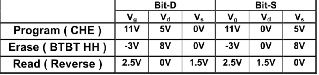
Table Captions Chapter 1 Table 1.1 Operating principles and bias conditions of an NBit cell. Chapter 6
Table 6.1 Devices used in the study. Vti means the initial-Vt of the cell. The channel
width is 0.18µm.
Table 6.2 Operating principles and conditions in this study.
Table 6.3 Comparison of neighboring junction bias effect among cells of various channel length and channel doping concentration.
Figure Captions Chapter 1 Fig.1.1 Schematic representation of an NBit cell. Fig.1.2 Concept of reverse read is depicted by the drain depletion region in which the effect of injected charges is screened out. Fig.1.3 Junction bias effect on the reverse read scheme.
Fig.1.4 (a) Definition of the forward- and the reverse-read Vt of Bit-S.
(b) ∆Vt-REV versus ∆Vt-FWD plot of the Bit-S in (a). Operating-Vt window is
saturated due to the so-called 2nd-bit effect.
Fig.1.5 Two-bit programming characteristics of an NBit cell. Firstly, Bit-D is programmed while Bit-S is at erase state. Then Bit-S is programmed while Bit-D has been at program state.
Fig.1.6 Two-bits erasing characteristics of an NBit cell.
Fig.1.7 Vt versus retention time of a fresh NBit cell. The bake temperature is 150C.
Fig.1.8 Endurance characteristics of an NBit cell.
Fig.1.9 Vt versus retention time of a 10K P/E cycled NBit cell. The storage
temperature is 25C. Fig.1.10 Representation of the reliability issues we have observed in an NBit cell. Chapter 2 Fig.2.1 Charge loss versus cycles of an NBit cell. The bake is at 150C for 24 hours. Fig.2.2 Program-state charge loss versus retention time in a fresh and a 100K P/E cycled NBit cells. T=25C and 85C.
Fig.2.3 (a) Concept of Vt-Vj measurement to explore the trapped electron extent in
an NBit cell.
(b) Illustration of Vt-Vj characteristics by which charge lateral extent can be
estimated. The dashed one has a wider electron distribution as shown in (a). Fig.2.4 (a) Charge-pumping current (Icp) measurement to characterize the localized
trapped charges nearby the injection junction.
(b) Trapped-hole (IcpE, open square) and trapped-electron (IcpP, open circle)
effect on the measured Icp characteristics.
and after 24 hours, 85C storage. The cell is at program state.
Fig.2.6 The measured charge-pumping current (Icp) versus the low level of gate
pulse (Vgl) in the CP measurement. The 100K cycled cell is at program state.
The bake time is 24 hours and the bake temperature is 85C. Fig.2.7 Program-state charge loss at different applied gate biases. T=25C. Fig.2.8 The CV temporal evolution of an ONO capacitor.
Fig.2.9 Evolution of the flatband voltage shift with the retention time in an ONO capacitor. The gate biases in measurement are 0, -2V, -4V, and -6V.
Fig.2.10 Illustration of nitride trapped charges escape via Frenkel-Poole emission and subsequent oxide defect-assisted tunneling.
Fig.2.11 The measured flatband voltage shift versus the square root of the nitride electric field which is proportional to (V0-Vg). V0 represents the internal
built-in field including the flatband voltage and the trapped charge effects. It is 5V in our example. The storage time is 10000 sec..
Fig.2.12 The charge retention lifetime versus applied gate bias. Retention lifetime is defined as the storage time sustained for ∆Vt=1V, 1.5V, and 2V,
respectively.
Fig.2.13 The retention lifetime versus (V0-Vg)1/2. V0 is 2V and 5V for the cell and
the capacitor, respectively. The retention lifetime is defined as the storage time sustained for a 1V shift of the Vfb of the capacitor or a 1V shift of the
Vt of the memory cell.
Fig.2.14 ∆Vt (by field acceleration) and ∆Icp,max versus cycle numbers of an NBit
cell.
Fig.2.15 Vt evolution with Vg-accelerating time of a fresh and a 10K cycled sectors.
Vg=-3V.
Fig.2.16 ∆<Vt> evolution with Vg-accelerating time of a 10K cycled sector. Vg= ñ3V
and ñ7V.
Fig.2.17 ∆<Vt> by field acceleration versus cycle numbers in a product.
Fig.2.18 (a) Program-state retention loss versus time at different temperatures. (b) Charge-pumping current in a fresh and a 100K P/E cycled cells. The
bake temperature is 150C.
Fig.2.19 Overall retention loss of various cycled sectors by 150C, 50 hours bake (∆<Vt(bake)>) with and without a preceding field acceleration of Vg=-3V,
18.5 hours (∆<Vt(field)>).
Fig.2.20 Overall retention loss of 10K cycled sectors by 150C, 50 hours bake (∆<VT(bake)>) with and without a preceding 18.5 hours field acceleration
of Vg=-3V and ñ5V (∆<Vt(field)>).
Fig.2.21 The retention loss of a 10K cycled cell, which is firstly accelerated by Vg=-3V for various time and then baked at T=150C for 50 hours, is
recorded. The variation of ∆Icp,max is also denoted.
Fig.2.22 (Following) ∆Vt(bake) versus (preceding) ∆Vt(field) of 10K cycled cells.
Bake is at 150C, 50 hours, and field acceleration is done by Vg=-3V
and ñ7V with various retention time.
Fig.2.23 Roles of oxide trap and interface state in the retention loss of an NBit cell. Fig.2.24 ∆Vt by field acceleration versus ∆Icp,max of an NBit cell.
Fig.2.25 Normalized ∆Icp,max versus cycle numbers of NBit cells fabricated by
various process conditions.
Fig.2.26 ∆Vt by high-temperature bake versus ∆Icp,max of 10K cycled cells of various
processes.
Chapter 3
Fig.3.1 Erase-state Vt drift versus retention time of a fresh and a 1K P/E cycled
NBit cells.
Fig.3.2 The Vt shift versus the retention time of 10K P/E cycles cells in erase state.
The bake temperatures are 25C, 85C, and 150C.
Fig.3.3 The measured Icp versus Vgh of a 100K P/E cycles cell in erase state. The
bake time is 4 hours and the bake temperature is 85C.
Fig.3.4 P/E cycling dependence of erase-state Vt drift after 104 sec. storage.
Fig.3.5 (a) The measured Vt and GIDL current of a fresh and a 1K P/E cycled NBit
cells.
(b) Proposed charge configuration according to the results in (a).
Fig.3.6 Schematic band diagram illustrating the positive oxide charge detrapping current (Ih) in an NBit cell.
Fig.3.7 Illustration of a charge separation technique. Isd is an electron leakage
Fig.3.8 The measured Ig and Ib transients in an ì erase-stateî capacitor. The capacitor
has a large gate area (2.5×105 µm2). Vg=Vfb in the measurement.
Fig.3.9 Pre-stress and post-stress substrate currents in two large area devices (500µm × 500µm). The FN stress condition is Vg=-18V for 3000s. Substrate current was measured at Vg=Vfb.
Fig.3.10 Room-temperature Vt drift versus time in two 10K P/E cycled cells
fabricated with different ONO processes. The cell size is Lg=0.5µm and Wg=0.35µm.
Chapter 4
Fig.4.1 The low bound of erase-state Vt distribution versus cycle numbers before
and after baking at 150C for 168 hours.
Fig.4.2 (a) Concept of Vcp and Vbtbt to estimate the stored charges above the channel
and the n+ junction, respectively. Charge-pumping characteristics (b) and GIDL current (c) are measured for a fresh NBit cell which is then over-erased and then baked at high temperature.
Fig.4.3 The required erase time versus cycle numbers corresponding to Fig.4.1. Fig.4.4 The required erase time versus cycle numbers of an emulating single cell. Fig.4.5 The extracted Vbtbt versus cycle numbers corresponding to Fig.4.4.
Fig.4.6 The evolution of Vt with the storage time in a strongly erased cell. The bake
temperature are 85C, 150C, and 250C. A negative Vt shift is observed.
Fig.4.7 Charge pumping characteristics of an NBit cell which is erased by 30 shots and then is baked at 150C for 15 minutes, 3 hours, and 37 hours, respectively.
Fig.4.8 Vbtbt is plotted against Vcp. A positive correlation is found between them.
Fig.4.9 Schematic representation of the lateral spread of trapped holes and the resulting channel shortening effect that cause the negative Vt drift in an
NBit cell.
Fig.4.10 ∆Vbtbt versus bake time at various temperatures. All curves follow a straight
line on a semi-log scale. The lines represent the calculated results.
Fig.5.1 Read disturb characteristics of a fresh cell and a 10K P/E cycled cells.Lg=0.5µm and Vg/Vd/Vs=2.5V/1.6V/0V.
Fig.5.2 Two-phase measurement of the Vt shift temporal evolution of a 10K P/E
cycled cell. In curve (a), the cell is at RT mode in the first 104 sec. and is at
RD mode in the following 104 sec. The sequence is reversed in curve (b). Bias conditions of RT and RD are Vg/Vd/Vs=0V/0V/0V and
Vg/Vd/Vs=3V/1.6V/0V, respectively. Lg=0.5µm.
Fig.5.3 Schematics of band diagrams and carrier transport mechanisms at various bias conditions. Solid circles represent the residual electrons in trapping nitride or channel electrons in silicon, and open circles represent the positive trapped charges in bottom oxide. φh and φe represent the hole and electron
tunneling barrier heights, respectively. mh and me represent the hole and
electron tunneling effective masses, respectively. Nox is the effective
positive oxide charge volumtric density. Three carrier transport paths are illustrated: (a) Positive oxide charge tunnel detrapping at low oxide field (Jh). (b) Positive oxide charge-assisted electron injection into nitride (Jcat), in
addition to Jh, at high oxide field. (c) Positive oxide charge-assisted
hot-electron injection into nitride (Jcat), in addition to Jh, at high lateral field.
Hot electrons are generated via lateral field heating. Time evolutions of these injection currents and Vt shifts are also formulated.
Fig.5.4 Vt shift versus applied gate bias of a 10K P/E cycled cell. The drain and the
source are grounded, and the disturb time is 104 sec. Lg=0.5µm.
Fig.5.5 (a) The measured Ig and Ib transients at erase state. The cell has a large gate
area (2.5×105 µm2). Vg is equal to Vfb, Vfb+3V, Vfb+6V, respectively.
(b) Field dependence of positive oxide charge detrapping current (Ib) and
electron tunneling current (Isd) at t=0.2 sec. in (a).
Fig.5.6 Vt shift versus applied gate bias of a 10K P/E cycled cell. The drain and the
source are grounded, and the disturb time is 104 sec. Lg=0.5µm.
Fig.5.7 Vt shift versus disturb time of a 10K P/E cycled cell at various drain biases.
Vg/Vs=3V/0V and Lg=0.5µm.
Fig.5.8 Read disturb induced Vt shift versus applied drain bias of a 10K P/E cycled
Fig.5.9 Read lifetime projection by Vd-accelerating approach. Read lifetime is
defined as the disturb time resulting in a Vt shift of 0.2V. Vg/Vs=3V/0V and
Lg=0.5µm. As shown in the figure, read lifetime is overestimated in the
low-Vd regime where gate-enhanced disturb dominates.
Fig.5.10 Vt shift versus disturb time of 1K P/E cycled cells with different channel
lengths. Vg/Vd/Vs=3V/1.6V/0V.
Fig.5.11 Temperature effect on read disturb of 1K P/E cycled cells. Devices with gate lengths of 0.5µm, 0.4µm and 0.3µm are characterized. The applied gate and drain biases are 3V and 1.6V, respectively, and the disturb time is 104 sec..
Fig.5.12 Initial threshold voltage versus room-temperature drift, gate disturb and read disturb. The cells undergo 10K P/E cycles. The bias conditions for GD, and RD are Vg-Vti/Vd/Vs=1.5V/0V/0V and 1.5V/1.6V/0V, respevtively, and
Vg=Vd=Vs=0V for RT. The disturb time is 104 sec. and Lg=0.5µm.
Chapter 6
Fig.6.1 EV-pass shot v.s. cycles of a 2Mb test chip. Here, the EV-pass shots mean the accumulated erase shots necessary for all the ì 1stî or the ì 2ndî bits of the chip to pass erase-verify (EV).
Fig.6.2 Schematic representation of an NBit cell structure and localized charges storage. The charge distributions are depicted for the case in which Bit-D is the 1st bit and Bit-S is the 2nd bit.
Fig.6.3 (a) Techniques to monitor the stored charge distribution in the trapping nitride. Charges stored above the channel region are estimated by Vt-REV
shift that induced a constant read current. Charges stored above the n+ junction are estimated by Vg shift that induced a constant GIDL current at
Vd=2V.
(b) Schematic representation of the net stored charge polarity above the channel and above the n+ region in a ∆Vt-REV-∆Vbtbt plot. Reverse-read Vt
(Vt-REV) is used here to measure the stored charged effect above the
conduction channel.
Fig.6.4 EV-pass shots v.s. P/E cycles of an NBit cell.
to Vd for Bit-D, and is equal to Vs for Bit-S. This result is at the 50th cycle.
Fig.6.6 ∆Vt-∆Vbtbt plot during programming of a fresh and a 50 P/E cycled NBit
cells.
Fig.6.7 Normalized electron temperature profiles (a), and electron density (electron energy > 3.2eV) distributions (b) along the conduction channel calculated by 2D device simulations. Vg/Vd=10/3.6V. For the 2nd bit, the neighboring
1st bit has been programmed to ∆V t=2V.
Fig.6.8 ∆Vt-∆Vbtbt plot during erasing of a fresh and a 50 P/E cycled NBit cells.
Fig.6.9 Comparison of the ∆Vt-∆Vj characteristics of a fresh and a 50 P/E cycled
NBit cells.
Fig.6.10 Schematic representation of the injected electron distribution after programming of a fresh and a 50 P/E cycled NBit cells.
Fig.6.11 Erase characteristics of cells of various Lg and Vti (Table 6.1). ∆Vt
representation the Vt shift from its programmed-stateís Vt after each erase
shot.
Fig.6.12 Erase speed comparison among various source junction biases during erasing the Bit-D of cell-A and cell-Bí. Vg/Vd=-6V/5V.
Chapter 1 Introduction 1.1 An Overview In the past decade, Flash memory market has been driven by cellular phone and other types of electronic portable equipment (MP3 audio player, digital camera, and so on). It would further explosively grow in mass storage applications such as memory card and removable storage (e.g. USB Flash driver). It reached a worldwide revenue of 12.4 billions in 2003 and is predicted to be 17.3 billions in 2004 [1.1].
Flash memory cell was firstly invented in 1984 [1.2]. It was realized by a 2µm triple poly-silicon technology with a cell size of 64µm2 to compose of a 256Kb chip [1.3]. It is based on the same concept of a floating-gate EPROM [1.4]. However, the erase is performed on a block of cells (or a whole chip) at the same time via electrical method. Such ì flash eraseî much increases the erase speed and thus earn the name after that. Excellent data retention is the most extinguishing feature of the ì nonvolatileî memory (NVM) (e.g. Mask ROM, PROM, EPROM, EEPROM) against the ì volatileî one (e.g. SRAM, DRAM). It means that, for example, the stored data can be retained more than 10 years even the ambient temperature is as high as 85C and the power supply is removed [1.5].
From the device structure point of view, floating-gate based [1.4] and SONOS-type cells [1.6] (evolved from the MNOS cells [1.7]) are the most matured which use floating poly-silicon and trapping nitride, respectively, as the charge storage media above the conduction channel of a MOSFET to modulate the memory cellís Vt. One
of the advantages of the charge trapping-storage cells over the floating-gate cells is their better resistance to charge loss via defects (oxide traps, pin holes) in the surrounding oxide [1.8]. Regarding the operating principles, hot-carrier injections [1.9-1.17] and Fowler-Nordheim (FN) tunnel injection [1.18-1.19] are used for both program and erase. Program to high-Vt state [1.2] and to low-Vt state [1.20] are also
proposed.
There are two major categories of Flash memory product. For ì codeî application, it is mostly composed of NOR-type arrays to have high random access speed. It advances from a 256Kb chip based on 1.5µm technology (cell size of 36µm2) in 1988
[1.21] to a cell size of 0.049µm2 based on 70nm technology in 2004 [1.22]. For ì data storageî application, it uses NAND-type arrays to have higher program/erase throughput and the smallest cell size. It advances from a cell size of 6.43µm2 based on 1µm technology in 1987 [1.23] to a 8Gb chip based on 63nm multi-level-cell technology (cell size of 0.0164µm2) in 2004 [1.24]. In all cases, low voltage/power
operation, small cell size, high program/erase/read speed, good endurance and retention are the dream targets for any kinds of Flash memory.
Floating-gate based cell is the mainstream technology till now. To meet the needs of high density and low cost, Flash product doubles its density as the technology node evolves to next generation [1.25]. The other density-increasing approach is by multi-level-cell (MLC) concept [1.26]. It means that, for example, 2 bits can be stored in a single memory cell. In this way, ì electricalî memory density can be doubled based on exactly the same ì physicalî cell and process technology. Still another way to increase the memory density is by storing bit information at physically different sites in a ì singleî memory cell. This concept has been applied to both floating-gate based [1.27] and trapping-storage based cells [1.28]. It can also have electrical multi-level in each sites to obtain 4-bit (or more) per cell [1.29].
1.2 Brief of the Trapping-Nitride Localized-Charge Storage Cell
Except for the higher packing density, localized charge trapping-storage cells (NROM [1.28], NBit [1.30], PHINES [1.31], microFlash [1.32], MirrorBit [1.28], TwinFlash [1.34]), which use hot-carrier injections for both programming and erasing, are more immune to charge loss since they have a sufficiently thick bottom oxide (>5nm) to avoid charge direct back tunneling [1.35], as comparing to conventional SONOS cells using uniform charge storage and FN-/modified-FN-tunnel injection/ejection of charge carriers through a much thinner tunnel oxide (~2nm) during programming/erasing. Furthermore, less process complex and absence of floating-gate coupling issue are also the advantages over the floating-gate cells [1.36]. In this way, trapping-nitride based, localized charge-storage Flash memory cell rivals recently and is considered to be a promising candidate of the high density Flash products [1.37-1.38].
Letís take a closer look at such a cell now. Fig.1.1 shows a typical NBit cell [1.30] (From now on, the memory cell discussed in this dissertation is named as the NBit
cell). It is made of an n-channel MOSFET with an oxide-nitride-oxide (ONO) gate structure. The charges are stored locally in the nitride layer above the channel region nearby the n+ source/drain junctions. Since the nitride is a dielectric film, the charge is immobile inside it. Long-term localized charge storage is thus workable. Once charges are stored locally in it, a reverse-read scheme is applied to sense the bit state [1.28]. It means that to read out the information stored in Bit-S (Bit-D), Vd
(Vs) is biased at 1.8V and Vs (Vd) is grounded (Fig.1.2). The applied Vd must be large
enough to ì screenî out the injected charge effect at the drain side (Bit-D). The read current (or threshold voltage) is then controlled by the stored charges at the source side (Bit-S), almost regardless of the charges at Bit-D. Fig.1.3 show the junction bias effect on the sensed Vt. Assuming Bit-S and Bit-D store a low-Vt state and a high-Vt
state, respectively (as shown in Fig.1.2). If the applied Vd is small (e.g. Vd
=0.1V), Bit-S would be incorrectly read as a high-Vt bit. However, if Vd is high enough (e.g.
Vd=1.5V), Bit-S can be correctly sensed as a low-Vt bit. Even so, the operating-Vt
window, which means the Vt difference between the high-Vt state and the low-Vt state,
is limited in such read scheme. Assuming there is no charges stored at Bit-S, and there are electrons stored at Bit-D (Fig.1.4 (a)). The sensed Vt of Bit-S, which is equal to
the applied Vg that conducts a channel current of 1µA, is defined to be Vt-REV and V t-FWD by applied 1.8V at drain side and at source side, respectively. Fig.1.4 (b) shows
the ∆Vt-FWD v.s. ∆Vt-REV plot in which each point represents various amounts of
electrons stored at Bit-D. If there are only few electrons distributed within the drain depletion region, the sensed ∆Vt-REV is close to 0V as expected while the ∆Vt-FWD is
proportional to the stored electron density at Bit-D. If there are more and more electrons stored at Bit-D, electron distribution would be wider and is beyond the drain depletion region at Vd=1.8V. ∆Vt-REV would increase with ∆Vt-FWD, which is
proportional to the stored electron density, with a slope of 1 on the ∆Vt-REV v.s. ∆V t-FWD plot. This is known as the 2nd-bit effect (Bit-D here) in the NBit technology [1.39].
The operating-Vt window which is equal to ∆Vt-REV-∆Vt-FWD is then saturated at 2V.
The last subject to realize 2-bit-per-cell is how to inject the charges locally into the trapping nitride. Channel-hot-electron (CHE) injection and band-to-band-tunneling (BTBT) induced hot-hole (HH) injection [1.28] are utilized for programming and erasing, respectively (Table 1.1). Carriers are heated by local electric field and then inject toward the gate nearby the junction and then are trapped
in the nitride. Since they are based on hot-carrier injection processes, the bottom oxide of this cell can be thicker to avoid charge direct back tunneling. Its intrinsic data retention is thus better than a conventional SONOS cell which using FN (or modified-FN) injection through a much thinner tunnel oxide. Fig.1.5 and Fig.1.6 show the program and erase characteristics, respectively, of this NBit cell. Two bits can be programmed independently and erase ì simultaneouslyî (since they belong to the same ì sectorî ).
Finally, the cell shows good intrinsic data retention before program/erase (P/E) cycles (Fig.1.7), and it is also demonstrated to be endurable more than 100K cycles (Fig.1.8). However, we find that data retention degrades as the cells undergo extensive P/E cycles. Fig.1.9 show the Vt evolution with the storage time of a 10K
P/E cycled cell. The ambient temperature is only at 25C. It is found that the program-state Vt drops down and the erase-state Vt drifts up with retention time. As these two
states approaches to each other, it may result in a wrong data sensing. We use Fig.1.10 to illustrate the reliability issues we have observed in this cell. They are cycling-induced high-state Vt loss, low-state Vt drift-up and drop-down, read disturb,
and erase speed degradation.
1.3 Organization of This Dissertation
We will address each issue in this dissertation, which is thus organized in the following manner. An overview of the Flash memory cell technologies and the concepts of a trapping-nitride localized-charge storage cell (the NBit cell here) and its reliability issues have been presented here. We will discuss the mechanisms that dominate the charge loss in chapter 2. In chapter 3, the charge gain behavior is addressed. Vt drop-down in an over-erased cell is characterized in chapter 4. Various
read disturb modes are modeled in chapter 5. We will disclose the causes of erase speed degradation in chapter 6. Conclusions follow in chapter 7.
two-bit-per-cell,
localized charge storage
O
N
O
n
+n
+G
S
D
Bit-S
(2
nd-bit)
Bit-D
(1
st-bit)
p-substrate
Fig.1.1 Schematic representation of an NBit cell.Fig.1.3 Junction bias effect on the reverse read scheme. Fig.1.2 Concept of reverse read is depicted by the drain depletion region in which the effect of injected charges is screened out.
O
O
N
e-
trapped electrons
low
high
depletion region
information
to be read
O
O
N
e-
trapped electrons
low V
dhigh V
ddepletion region
to be read
Bit-S
Bit-D
O
O
N
e-
trapped electrons
low
high
depletion region
information
to be read
O
O
N
e-
trapped electrons
low V
dhigh V
ddepletion region
to be read
Bit-S
Bit-D
0.0
0.4
0.8
1.2
1.6
2.0
1.5
2.0
2.5
3.0
3.5
4.0
4.5
5.0
5.5
V
tof
Bit-S
(V
)
V
d(V)
Fig.1.4 (a) Definition of the forward- and the reverse-read Vt of Bit-S.
(b) ∆Vt-REV versus ∆Vt-FWD plot of the Bit-S in (a). Operating-Vt window is
saturated due to the so-called 2nd-bit effect. (a) (b)
O
O
N
trapped electrons
@ Bit-D
e-V
t-REVof Bit-S
by V
d=1.8V
O
O
N
V
t-FWDof Bit-S
by V
s=1.8V
D
S
information @ Bit-S
to be read
O
O
N
trapped electrons
@ Bit-D
e-V
t-REVof Bit-S
by V
d=1.8V
O
O
N
V
t-FWDof Bit-S
by V
s=1.8V
D
S
information @ Bit-S
to be read
0.0 0.5 1.0 1.5 2.0 2.5 3.0 3.5
0.0
0.5
1.0
1.5
2.0
2.5
3.0
3.5
∆
V
t-R E V(V)
∆
V
t-FWD(V)
slope ~ 1
slope << 1
Table 1.1 Operating principles and bias conditions of an NBit cell. Bit-D Bit-S
Vg Vd Vs Vg Vd Vs
Program ( CHE )
11V 5V 0V 11V 0V 5VErase ( BTBT HH )
-3V 8V 0V -3V 0V 8VRead ( Reverse )
2.5V 0V 1.5V 2.5V 1.5V 0VFig.1.6 Two-bits erasing characteristics of an NBit cell. Fig.1.5 Two-bit programming characteristics of an NBit cell. Firstly, Bit-D is programmed while Bit-S is at erase state. Then Bit-S is programmed while Bit-D has been at program state.
10
-710
-610
-510
-410
-310
-22
3
4
5
6
7
V
t(V
)
Erase Time (sec.)
Bit-D
Bit-S
Both Bit-D and Bit-S are erased
simultaneously
Both ERS Bit-S Bit-D D S10
-710
-610
-510
-410
-310
-22
3
4
5
6
7
V
t(V
)
Erase Time (sec.)
Bit-D
Bit-S
Both Bit-D and Bit-S are erased
simultaneously
Both ERS Bit-S Bit-D D S Both ERS Bit-S Bit-D D S D S0
1
2
3
4
2
3
4
5
6
7
V
t(V
)
Program Time
(
µs
)
Bit-D Bit-S solid: firstly Bit-D is programmed open: then Bit-S is programmed Bit-D PGM Bit-S ERS Bit-S Bit-D D S Both PGM Bit-S Bit-D D S0
1
2
3
4
2
3
4
5
6
7
V
t(V
)
Program Time
(
µs
)
Bit-D Bit-S solid: firstly Bit-D is programmed open: then Bit-S is programmed Bit-D PGM Bit-S ERS Bit-S Bit-D D S Bit-D PGM Bit-S ERS Bit-S Bit-D D S D S Both PGM Bit-S Bit-D D S Both PGM Bit-S Bit-D D S D S
10
010
110
210
310
410
510
60
1
2
3
4
5
6
7
erase state
program state
V
t(V
)
P/E Cycles
10
010
110
210
310
410
510
60
1
2
3
4
5
6
7
erase state
program state
V
t(V)
Retention time (sec.)
Fig.1.7 Vt versus retention time of a fresh NBit cell. The bake temperature is 150C. Fig.1.8 Endurance characteristics of an NBit cell.Fig.1.9 Vt versus retention time of a 10K P/E cycled NBit cell. The storage temperature is 25C.
Program-state V
tdrops
down!
100 101 102 103 104 105 0 1 2 3 4 5 6 7V
t(V
)
Retention time (sec.)
program state erase stateErase-state V
tdrifts up!
Fig.1.10 Representation of the reliability issues we have observed in an NBit cell.
P/E cycles
Storage time
V
t High-state Vtloss Low-state Vtdrift-up, and Read disturb Low-state Vtdrop-down Cycling window degradation (Erase speed degradation) Over erase Operating-VtwindowP/E cycles
Storage time
V
t High-state Vtloss Low-state Vtdrift-up, and Read disturb Low-state Vtdrop-down Cycling window degradation (Erase speed degradation) Over erase Operating-VtwindowChapter 2 Charge Loss in a High-Vt Cell 2.1 Motivation In previous chapter, we have showed that a fresh cell has good charge retentivity (Fig.1.7). However, charge retention in a P/E cycled cell degrades (Fig.1.9). Fig.2.1 shows that charge loss increases with cycle numbers. In addition, this charge loss exhibits strong temperature dependence (Fig.2.2).
It is still controversial about the mechanisms to explain the observed charge loss in the localized trapping-storage cells. Saifunís group has proposed that thermionic emission and then re-distribution or leak-out of the stored electrons are the cause of Vt
loss in an un-cycled cell [2.1]. They also claimed that lateral re-distributions of the trapped charges, especially some residual holes, account for the Vt loss in a cycled
one [2.2-2.3]. However, we do not find any direct evidence of ì netî residual holes in a cycled cell which is at program state. Meanwhile, we find that the Vt loss is strongly
dependent on the applied Vg bias during retention test. Charge loss along the vertical
direction is suspected. In the following sections, we would develop the models in detail.
2.2 Experimental
2.2.1 Device Samples
The cell used in this work (and in the dissertation) is made of an n-channel MOSFET with an oxide-nitride-oxide (ONO) gate dielectric structure (Fig.1.1). Typically, the thickness of each ONO layer is 9nm (top oxide), 6nm and 6nm, and Wg/Lg is 0.38µm/0.48µm. An ONO capacitor (2.5×105 µm2) with uniform stress and
charge storage is also used. The effect of lateral charge migration can be excluded in this device. The evolution of the flatband voltage (Vfb) of the ONO capacitor with
time is monitored to study the charge retention behavior. Finally, a 64Mb chip with a sector size of 512Kb which is composed of such cells is also characterized. It is used to demonstrate that the observed phenomena in a single cell and the utilized methods to characterize it are consistently applicable to a real product.
2.2.2 Characterization Techniques
Two specific methods are utilized to study the lateral spreading of the injected carriers. Assuming that electrons are trapped in the nitride layer above the channel nearby the junction, a Vt versus Vj measurement is used to investigate the lateral
extent of the trapped electrons (Fig.2.3 (a)). Here, Vt is defined as the applied gate
voltage that induces a drain current of 1µA. These trapped electrons will raise the potential barrier nearby the injection junction. An increased Vt, which is proportional
to the trapped electron density, will be measured at a low junction bias (Vj1 in Fig.2.3).
As a sufficiently high junction bias (Vj2 in Fig.2.3) is applied, the junction depletion
region will extend toward the channel. The trapped electrons will have little effect on the measured I-V characteristics when they are located within the junction depletion region [2.4]. The trapped electron density and its lateral extent can be estimated by this measurement (Fig.2.3 (b)).
A charge-pumping (CP) method [2.5], which is also able to probe the lateral distribution of trapped charges, is also used. Letís see Fig.2.4 (a). A trapezoidal pulse train (Gate pulse P) with a fixed high level (Vgh) and successively decreasing low
levels (Vgl) is applied to the gate of the device. The substrate and the drain are
grounded and the source is floating. The charge-pumping current IcpP (=Id=Ib) versus
Vgl is measured. The fixed Vgh is sufficiently high to ensure that the entire channel is
inverted. By varying Vgl, only the part of channel that undergoes
inversion-accumulation-inversion over a pulse cycle contributes to IcpP. Since the trapped
electrons (near the drain side) cause an increase of the local flatband voltage, an IcpP
shift along the Vgl axis will be observed in a programmed cell. Based on the measured
IcpP versus Vgl curves of an un-programmed and a programmed cells (Fig.2.4 (b)), the
trapped electron density can be extracted [2.5]. The trapped hole density can be profiled in a similar manner by a pulse train with a fixed low level and successively increasing high levels (Gate pulse E in Fig.2.4 (a)) applied to the gate. The lateral migration of trapped charges in both the program and the erase states can also be estimated by this technique.
We use the Vt versus Vd characteristics to give an indication of the density and the
lateral extent of the trapped electrons in a programmed cell. Fig.2.5 shows the Vt-Vd
characteristics of a 100K P/E cycled cell in the program state before and after 24 hours storage. The storage temperature is 85C. It can be seen that the Vt has dropped
due to charge loss, however, the shape of Vt versus Vd curves is essentially unchanged
and there is no crossover in the Vt versus Vd characteristics before and after 85C, 24
hours storage. This indicates that lateral migration of electrons does not occur. We have also applied the charge-pumping technique to probe the lateral electron extent (Fig.2.6). If the trapped electrons spread laterally during the storage period, an increased Icp will be observed due to the extension of the trapped electron area. As
indicated in Fig.2.6, the leftward shift of the Icp implies a decrease of the trapped
electron density. However, no clear evidence of lateral electron movement is shown in the charge-pumping characteristics. On the other hand, we find the charge loss is strongly dependent on the applied vertical field during the retention test (Fig.2.7). It gives us a hint that the stored charges may leak out along the vertical direction: from the trapping nitride through the bottom oxide to the substrate.
In order to correlate the Vt loss to charge escape through the bottom oxide, the
temporal evolution of the flatband voltage of an ONO capacitor was measured (Fig.2.8). The ONO capacitor has undergone a negative gate stress (-100nA for 1000 seconds, to emulate the P/E cycling effect) and then was programmed to a high-Vt
state by +FN injection. Since the structure has uniform charge storage, lateral re-distribution effect of the stored charges can be excluded. Charge loss through the bottom oxide should be the only cause for the flatband voltage shift. The gate bias in the measurement is from Vg=0V to Vg=-6V. The measured results are shown in
Fig.2.9. The flatband voltage shift indeed exhibits vertical field dependence, which is similar to the Vt loss behavior we observed in a single cell (Fig.2.7). 2.3 Charge Loss Model We thus propose the physical mechanism to explain the charge loss behavior in a P/E cycled cell, as shown in Fig.2.10. The field- and temperature-accelerating effects and the cycling-enhanced effect on the charge loss suggest that the nitride charge escape is through thermionic-field emission and subsequent oxide trap-assisted tunneling. Frenkel-Poole model has been recognized to be the dominant charge carrier transport mechanism in nitride [2.6]. According to the model, the emission time
constant τen of an electron in a nitride trap of energy depth of φen below the nitride conduction band edge can be expressed as: ) exp( ) ( 0 kT qE q n n en en en en πε φ τ φ τ − = (2.1),
where En is the nitride field and εn is the nitride dielectric constant. If the trapped
electron density (corresponding to the trap level of φen) is Nen0 right after
programming, it will evolve with time as: ) ) ( exp( ) ) ( exp( ) 0 , ( ) , ( 0 en en en en en en en en en t N t N t N φ τ φ τ φ φ = − = − (2.2).
In a Frenkel-Poole emission limited condition (i.e, τox in Fig.2.10 sufficiently fast),
the nitride charge escape current can be derived as: t kT N d t N d dt t dN t I en en en en en en en en en en 0 0 exp( ( )) ( ) ) ( ) ( ∝
∫
∝∫
− ∝ φ τ φ φ τ φ (2.3),assuming that the trapped electron distribution (right after programming) is continuous in the energy spectrum and is with a constant trapping density (Nen0) in the
nitride. The corresponding Vt loss would be: )] ln( [ ) ( ) ( ) ( 0 0 en n n en en en t t kT qE q N dt t I t Q t V τ πε + ∝ ∝ ∆ ∝ ∆
∫
(2.4).According to Eq. (2.4), Vt and Vfb evolution is linearly dependent on log(t), which
is as shown in Fig.2.7 and Fig.2.9 for a single cell and a capacitor, respectively. Besides, the charge loss is proportional to the square root of the nitride field, which is proportional to (V0-Vg). This is shown in Fig.2.11. Here, V0 is the built-in potential,
including the flatband voltage and trapped charge effects, at program state. From a 2D device simulation [2.7], V0 is around 2V in the single cell and 5V in the capacitor.
Learning from Fig.2.7, it is apparent that Vg is an effective accelerating factor for
retention lifetime measurement. If we assume that during the discharge time tѽ all the nitride traps with time constants less than tҏ will be completely emptied and all other traps will be unaffected, the memory retention time will be equal to the nitride charge detrapping time (we assume oxide trap assisted tunneling is sufficiently fast.). According to Eq. (2.1), we would further expect that: β ∝ −Vg V d Lifetime d 0 ) log( (2.5), where ono NT q kT q e πε β =log( ) (2.6),
by En=(V0-Vg)/Tono. Here, Tono is the equivalent thickness of the ONO stack. β is
calculated to be 2.6 decade/V0.5 in our sample.
In Fig.2.12, we plot the retention lifetime versus (V0-Vg)0.5. The symbols represent
the measured result. The extracted slope in Fig.2.12 is about 2.75 decade/V0.5 which is close to the theoretical value of 2.6 decade/V0.5. The extrapolated memory retention time at Vg=0V is about 107 sec. for ∆Vt=1.5V and is above 10 years for ∆Vt=2.0V.
We have also plotted the retention lifetime versus (V0-Vg)0.5 of an ONO capacitor as
shown in Fig.2.13. The slope is 2.49 dec/V0.5 which is quite close to the theoretical value (2.6 decade/V0.5) and the slope of a memory cell (2.75 decade/V0.5). It implies that the vertical charge loss occurs in an ONO capacitor with uniform charge storage and also in a memory cell with localized charge storage.
In this model, cycling-induced oxide defect is considered to be the stepping stone of the charge loss. Fig.2.14 shows the increase of the charge-pumping current (right axis) of the cell versus cycle numbers. The charge-pumping current is a direct measurement of the density of the interface states (Nit). It can be found that Icp,max
(Fig.2.4(b)) increases with cycle numbers. The growth rate follows a power law with the power factor of 0.5. It is quite consistent with the generation of interface states in a stressed NMOSFET [2.8], which implies that the bottom oxide is damaged during
P/E cycling. It is also suggested that bulk oxide defects (Qox) are also created
meanwhile [2.9]. However, itís hard to measure the bulk oxide trap density directly. We plot the charge loss versus cycle numbers on a log-log plot (Fig.2.14, left axis). A power law dependence with the power factor of 0.24, which is quite close to the generation rate of bulk oxide traps in a stressed NMOSFET [2.8], is obtained. It provides an indirect evidence of the role of oxide trap and its generation during P/E cycling.
2.4 Product Demonstration
The model is successful verified by a single cell and a capacitor. We would like to apply the same field accelerating method to a memory array under real product operation. A 64Mb chip used in this study is fabricated by 0.25µm process with a sector size of 512Kb. The cycling is performed on a MOSAID tester [2.10] and all bits are programmed and erased within one cycle. During retention test, checker-board pattern is used. In other words, each cell has one programmed bit and one erased bit at the same time.
In Fig.2.15, the Vt evolution with retention time at Vg=-3V is measured for a chip
before and after 10K cycles. Charge loss is observed for the cycled high-Vt cells. To
simplify the notation, the <Vt> is used to represent the mean value of the high-Vt
distribution. In Fig.2.16, the field-accelerating effect on the ∆<Vt> is observed and the
dependence is quite similar to the single cellís results (Fig.2.7). At both cases, charge loss increases with increasing vertical field. In Fig.2.17, the cycle number dependence of the ∆<Vt> is measured at Vg=-7V. The charge loss increases with the cycle number
and a power law dependence with the power factor of 0.223 is observed. Once again, it is close to the power factor of 0.29 obtained in a single cell (Fig.2.14). From Fig.2.15 to Fig.2.17, we know that the single cell and the product are well-correlated, and the validity of field acceleration is confirmed at product level as well as in a single cell.
2.5 Temperature Effect
The temperature-accelerating method is widely used in the retention test of a floating-gate cell [2.11]. We also investigate such application. Fig.2.18 shows the charge loss versus time at T=25C, 85C and 150C, respectively. In addition to the
strong dependence on the bake temperature, the retention loss at 150C shows a saturation behavior. Further study by using a charge-pumping technique reveals that amounts of the interface traps are annealed (Fig.2.18 (b)). We would suspect that trap annealing effect plays a role during the high-temperature bake period.
Letís also apply the high-temperature baking test to a chip. The chip firstly undergoes 10K P/E cycles. Two kinds of retention test procedure are compared. One is purely to bake the chip at 150C for 50 hours, and the other is to apply an extra field acceleration (by Vg=-3V, 18.5 hours) to the chip before baking.
In Fig.2.19, the ∆<Vt>ís of sectors with and without a preceding field acceleration
are compared after baking. ∆<Vt(field)> and ∆<Vt(bake)> represent Vt loss due to
field acceleration and bake, respectively. Fig.2.20 shows similar results of different accelerating vertical field. Some interesting phenomena are observed. Firstly, regardless of cycle numbers, ∆<Vt(bake)> is reduced if a preceding field acceleration
has been applied. Secondly, the overall retention loss is similar for both cases at low cycle numbers, however, it is larger for the field-acceleration-and-then-bake one after 10K cycles. Thirdly, charge loss by field acceleration (∆<Vt(field)> by Vg=-5V, 18.5
hours) could be larger than that by high-temperature bake only (∆<Vt(bake)> at
T=150C, 50 hours without a preceding field acceleration) as shown in Fig.2.20. And finally, the same ∆<Vt(bake)> (~0.2V) is found in 10K cycled sectors after strong
field acceleration, though the accelerating field and ∆<Vt(field)> are quite different
(Fig.2.20).
To investigate the relationship between these two accelerating methods, emulated single cells are firstly cycled up to 10K times. Retention loss is measured firstly by a negative-Vg acceleration with various time, and then by another high-temperature
bake at T=150C for 50 hours, as illustrated in Fig.2.21. The ∆Icp,maxís before and after
baking are also described. The overall Vt loss (∆Vt(field)+∆Vt(bake)) is a constant
value (~0.5V) as ∆Vt(field) is less than 0.3V, and it drops further (about additional
0.2V) when ∆Vt(field) exceeds 0.5V. If the two accelerating factors, temperature and
field, are interchangeable, ∆Vt(bake) will increase with decreasing ∆Vt(field). In
Fig.2.22, ∆Vt(bake) following various field-accelerating conditions is collected and is
plotted along with its preceding ∆Vt(field). ∆Vt(bake) shows a negative linearly
correlation with ∆Vt(field) as ∆Vt(field) is less than 0.5V. It implies that both methods