國
立
交
通
大
學
光電工程研究所
博
士
論
文
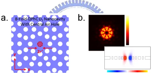
具耳語廊模態之光子晶體共振腔元件特性之研究
Researches on Photonic Crystal Microcavities and Devices Based on
Whispering-Gallery Modes
研 究 生:盧贊文
指導教授:李柏璁 教授
具耳語廊模態之光子晶體共振腔元件特性之研究
Researches on Photonic Crystal Microcavities and Devices Based on
Whispering-Gallery Modes
研 究 生:盧贊文 Student:Tsan-Wen Lu
指導教授:李柏璁 博士 Advisor:Dr. Po-Tsung Lee
國 立 交 通 大 學
光電工程研究所
博 士 論 文
A Dissertation
Submitted to Institute of Electro-Optical Engineering College of Electrical Engineering and Computer Science
National Chiao Tung University in partial Fulfillment of the Requirements
for the Degree of Doctor of Philosophy in
Electro-Optical Engineering July 2009
Hsinchu, Taiwan, Republic of China
具耳語廊模態之光子晶體共振腔元件特性之研究
學生:盧贊文
指導教授:李柏璁 博士
國立交通大學光電工程研究所博士班
摘
要
耳語廊模態所具有的高 Q 值與其多方向性共振是十分適合整合於積體光路中作為 光源或具有特定功用的被動元件。在本論文中,我們設計、製作、量測並分析各種具有 耳語廊模態的光子晶體共振腔元件特性,並探討其可能的應用。 論文一開始我們介紹了二維光子晶體共振腔元件相關的研究方法,包括數值模擬、 製程技術以及量測系統。首先,本論文基於一種八對稱準光子晶體設計具有耳語廊模態 的奈米共振腔,並在有限時域差分模擬與實驗上探討耳語廊模態的雷射特性、旁模抑制 機制以及極小的元件尺寸。此外,論文中也探討一種新穎且具有等向均勻性光能隙的環 形光子晶體,並設計出具有高Q 值耳語廊模態的微共振腔雷射元件。 利用具有高對稱性的十二對稱準光子晶體晶格,我們設計具有高 Q 值的耳語廊模態 雷射共振腔,並探討模態對共振腔邊界的強烈依存性,同時我們也進一步設計並探討多 共振腔耦合的雷射元件。而由於耳語廊模態的分佈特性,吾人可以在該共振腔下製作一 奈米柱作為電激發結構中的電流導路以及散熱器。透過製作不同尺寸的奈米柱,我們在 模擬與實驗上探討由奈米柱所造成耳語廊模態的光學衰減與熱導改善特性。 基於整合在一般光子晶體積體光路的理由,我們將準光子晶體共振腔的共振腔邊界 移植到一般光子晶體共振腔中以增強其中的耳語廊模態。藉由耳語廊模態的存在,我們 探討了在不同共振腔-波導耦合排列下的均勻光耦合特性。而在應用上,我們提出並探 討將此共振腔設計於雙層結構上,以作為高靈敏度光學應力偵測器的可能。最後,我們 在正方晶格光子晶體上設計一具有最低階耳語廊模態的奈米共振腔,此耳語廊模態在具 有較小模態體積的同時,同時具有較大的共振腔下奈米柱容許度。
Researches on Photonic Crystal Microcavities and Devices Based
on Whispering-Gallery Modes
student:Tsan-Wen Lu
Advisors:Dr. Po-Tsung Lee
Institute of Electro-Optical Engineering,
National Chiao Tung University
Abstract
Whispering-gallery (WG) mode with high quality (Q) factor and multi-directional resonance is very suitable for serving as the active laser sources and passive devices with specific functionalities in photonic integrated circuits (PICs). In this dissertation, we design, fabricate, and characterize various photonic crystal (PhC) based micro- and nano-cavities with high Q WG modes. The possible applications are also investigated and discussed.
In the beginning of this dissertation, we introduce the related research resources for researches on two-dimensional PhC cavity devices, including numerical simulation methods, nano-fabrication processes, and measurement systems. At first, we propose a nanocavity design with WG mode based on 8-fold quasi-PhC (QPhC). Various WG modal properties are addressed both in experiments and simulations, including single mode lasing actions, side mode reduction mechanism, compact device size, and so on. Besides, we also investigate a novel circular-PhC (CPhC) lattice structure with isotropic photonic band gap effect and characterize the designed CPhC microcavity with high Q WG mode.
By using 12-fold QPhC lattice structure with high symmetry, we design a microcavity with high Q WG mode. WG mode lasing actions and the strong mode dependence on microcavity boundary are confirmed. Due to the WG mode field distribution, we insert a nano-post beneath the microcavity to serve as the current injection pathway and heat sink in electrically-driven structure. By fabricating microcavities with different nano-post sizes, we investigate the WG modal loss behaviors and heat sink improvement due to nano-post both in experiments and simulations.
For the purpose of integration in PhC-based PICs, we project the 12-fold microcavity boundary on a PhC microcavity and enhance a high Q WG mode in it. Due to the presence of WG mode, we investigate the uniform coupling properties of different waveguide-cavity
geometries. In applications, we propose a double-layered structure based on above PhC microcavity and investigate its possibility in serving as an optical stress sensor. In the end, we propose a nanocavity design with lowest order WG mode based on square PhC lattice. This WG mode can be with very small mode volume and large nano-post tolerance beneath the nanocavity at the same time.
Acknowledgements
首先我要感謝我的指導教授 李柏璁 博士,在博士班的四年期間給予我在研究上非 常充足的自由度,除了在研究方向與題目上所給予的珍貴意見外,研究過程中不時的鞭 策,讓我在研究的路上不斷的向更高更遠的地方望去。而您適時的貼心鼓勵與對我駑鈍 的包容,更是讓我銘感五內,在此跟您致上我深深的謝意。 在實驗上,我要特別感謝交通大學奈米科技中心 李建平 教授在製程資源建立上莫 大的協助,還有交通大學光電系 盧廷昌 教授與交通大學電子系 林聖迪教 授在磊晶材 料上的提供。同時我由衷的感謝國科會在經費上的支援與補助 (計畫編號:NSC-97- 2120-M-009-004, NSC-96-2120-M-009-010, NSC-95-2221-E-009-056-MY3, NSC-95-2221- E-009-234, NSC-94-2215-E-009-016),讓我在博士班進行研究的期間能得到充足的設備 經費與資源。 我也要向一路走來的實驗室伙伴們致上深深的感謝。阿懋、佳禾、仲銓、嘉銘、老 漢、施大師、孟穎、何卡拉跟蕭大師,感謝你們這些學弟妹一路來在實驗上的幫忙與討 論,沒有你們,我想我的博士論文不會完成得如此順利。思元跟明璽,雖然你們對我的 論文一點貢獻都沒有,但是沒有你們閒暇時了無建設性的聊天打屁,我無法想像博士班 的生活會少掉多少歡笑聲。當然還有其他曾一起在實驗室打拼的伙伴們,我非常榮幸曾 經跟你們一起共事過,在此也跟你們說聲:謝謝! 最後,我要感謝一路以來在背後默默支持我的父母與小妹,你們簡單卻溫暖的關心 是讓我在研究路上走下去,最純粹也最強大的動力來源。當然還有我最愛的小練,妳的 笑顏總能把我從研究過程中的沮喪與不如意中拉回平靜,讓我有滿滿的勇氣繼續迎接太 陽升起的每一天。 盧贊文。2009 年 7 月 謹誌於 新竹交通大學
Table of Contents
Abstract (in Chinese) ……… i
Abstract (in English) ……… ii
Acknowledgements ……… iv
Table of Contents ……… v
Table Captions ……… vii
Figure Captions ……… viii
Chapter 1 Introduction 1 1-1 1-2 1-3 1-4 Micro Photonics……… Photonic Crystal……… Photonic Crystal Micro- and Nano-cavities…...……..……… Motivation and Dissertation Overview..…………..………… 1 2 5 7 Chapter 2 Modeling, Fabricating, and Characterizing Photonic Crystal Micro- and Nano-cavity Lasers 10 2-1 Numerical Methods………..……… 10
2-1-1 Plane-Wave Expansion Method………….……..………… 11
2-1-2 Finite-Difference Time-Domain Method……….………… 13
2-1-3 Simulation of Photonic Crystal Device………...…………. 15
2-2 Nano-Fabrication of Two-Dimensional Photonic Crystal Cavities……….……….. 18 2-3 2-3-1 2-3-2 2-4 Measurement Setup……….…………. Near-Infrared Micro-Photoluminescence System………… Systematic Accessories………...………. Summary……….……… 21 21 23 24 Chapter 3 8-Fold Quasi-Photonic Crystal Nanocavity & Circular
Photonic Crystal Microcavity with Whispering-Gallery
Modes 26
3-1 3-2
Quasi-Photonic Crystals……….. 8-Fold Quasi-Photonic Crystal Single-Defect Nanocavity..…
26 27 3-2-1 3-2-2 3-2-3 3-3 3-3-1 3-3-2 3-4
Cavity Design, Simulated, and Measured Modal Properties………...……….. Side-Mode Reduction Mechanism……… Compact Device Size………. Circular Photonic Crystal C2 Microcavity…..……….
Circular Photonic Crystal and Its PBG Effect………….. Microcavity Design & Modal Behavior……….. Summary……… 27 30 33 35 35 38 41
Chapter 4 Whispering-Gallery Mode in 12-Fold Quasi-Photonic Crystal Microcavity 42 4-1 4-1-1 4-1-2 4-1-3
12-Fold Quasi-Photonic Crystal D2 Microcavit…………..…
Microcavity Design, Simulated, and Measured Modal Properties……….. WG Mode Dependence on Cavity Geometry……… Coupling Microcavity Devices………..……….
42 43 43 49 4-2 4-2-1 4-2-2 4-2-3 4-3
Nano-Post Structure in 12-Fold Quasi-Photonic Crystal D2
Microcavity……….. Influences on Optical and Thermal Properties by Nano-Post……….. Nano-Post Fabrication……….. Measured Modal and Thermal Properties………….……. Summary……… 52 53 57 58 63 Chapter 5 Whispering-Gallery Modes in Photonic Crystal-Based
Micro- and Nanocavities 65
5-1 5-1-1 5-1-2 5-1-3
Photonic Crystal CD2 Microcavity……….
Microcavity Design & Simulated Modal Propertie..…….. Measured Lasing Action & Mode Identification…………. Uniform Coupling Properties……….
65 66 68 70 5-2 5-2-1 5-2-2 5-3 5-3-1 5-3-2 5-4
Photonic Crystal CD2 Microcavity for Stress Sensor
Applications………. Principle of Optical Stress Sensor………..………….…. Structure Design, Simulated Modal Behaviors, and Sensing Resolution………..….. Photonic Crystal Point-Shifted D0 Nanocavity……….
D0 Nanocavity Design & Simulated Modal Properties….
Measurement Results & Discussions……….. Summary……… 74 75 76 83 83 88 89
Chapter 6 Conclusion & Future Works 90
6-1 6-2
Conclusions……….………. Future Works & Suggestions………..
90 92
References ……….……… 93
Table Captions
Chapter 4
Table. 4-1: Table. 4-2: Table. 4-3:Observed lasing actions of 12-fold QPhC D2 microcavity lasers with
different variation regions and degrees. Over 300 devices are measured.
Coefficients for different materials used in heat transfer simulation (in M.K.S. unit).
Lasing properties of 12-fold QPhC D2 microcavity with different
nano-post sizes. 49 56 60
Chapter 5
Table. 5-1: Table. 5-2: Table. 5-3:Transmissions and wavelengths of different waveguide-cavity-waveguide geometries named A1 to A10 type.
Material parameters for silicon and InGaAsP used in FEM simulation. (a) Q factor, (b) mode volume, and (c) Purcell factor of WG2, 1, Dipole,
monopole mode in PhC D0 nanocavity, and WG2, 1 mode in PhC D1
nanocavity under different inserted nano-posts beneath.
73
80 87
Figure Captions
Chapter 1
Fig. 1-1:
Fig. 1-2:
Schemes of (a) line-defect for waveguide and (b) point-defect for cavity based on 2D triangular PhC lattice structure.
Scheme of 2D PhC nanocavity firstly demonstrated by O. Painter et al. [8] 5 6
Chapter 2
Fig. 2-1: Fig. 2-2: Fig. 2-3: Fig. 2-4: Fig. 2-5: Fig. 2-6: Fig. 2-7: Fig. 2-8: Fig. 2-9:Schemes of Yee cell in FDTD algorism.
Scheme of leapfrog time-stepping in FDTD algorism.
(a) Scheme of 2D triangular PhC lattice and (b) the corresponding PWE and FDTD simulated PBG effect.
(a) Scheme of optimized high Q PhC L3 microcavity. (b) 3D FDTD
simulated resonance spectrum and main resonance mode profile in electric field.
Designed epitaxial structure of InGaAsP MQWs, which is grown by Union Optronics Corporation, Taiwan. The PL spectrum centered near 1550 nm with 200 nm spectral span is also confirmed.
The overview of the fabrication process of 2D PhC microcavity. The insets A to D show the SEM pictures of each PhC pattern transferring step during the fabrication process.
(a) Scheme and (b) photo of NIR confocal micro-PL system setup.
The measured resonance spectrum from PhC D3 microcavity laser. The
SEM picture of Ph D3 microcavity is also shown in the inset.
Various sample stage accessories of NIR confocal micro-PL system, including (a) gas detection chamber, (b) current injection platform, (c) substrate temperature controlling system, and (d) in-plane laser emission collection stage. 14 15 16 18 19 20 21 23 24
Chapter 3
Fig. 3-1: Fig. 3-2: Fig. 3-3: Fig. 3-4: Fig. 3-5: Fig. 3-6: Fig. 3-7: Fig. 3-8: Fig. 3-9:Lattice structures of (a) penrose (5-fold), (b) octagonal (8-fold), and (c) dodecagonal (12-fold) QPhCs.
(a) Scheme of original 8-fold QPhC D1 nanocavity by removing a central
air hole and (b) the sustained dipole mode profile in magnetic field by FDTD simulation.
(a) Scheme of 8-fold QPhC D1 nanocavity by shifting the eight nearest air
holes from original positions A to B. (b) FDTD simulated WG4, 1 mode
profiles in electrical field in x-z and x-y planes well-sustained in 8-fold QPhC D1 nanocavity with modification.
(a) Top-view SEM picture of the designed 8-fold QPhC D1 nanocavity. The
inset shows its titled-view image. (b) Titled-view SEM image of 8-fold QPhC D1 nanocavities with lattice periods of eight to four from top to
bottom.
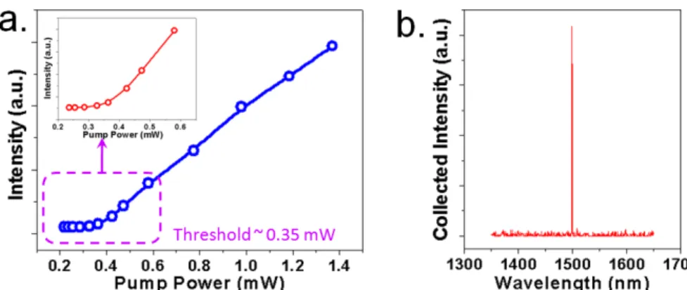
(a) The measured L-L curve of 8-fold QPhC D1 nanocavity. The inset
shows the L-L curve near threshold and indicates its threshold as low as 0.35 mW. (b) The measured lasing spectrum at 1499 nm with SMSR of 25 dB.
Defect modes in normalized frequency of 8-fold QPhC D1 nanocavity as a
function of r/a ratio. The PS denotes the phase-shifting mode [61]. The solid spheres denote the measured data, which match with WG4, 1 mode
quite well.
(a) Scheme of an 8-fold QPhC D1 nanocavity with central disturbance (air
hole inside or nano-post beneath). (b) FDTD simulated WG4, 1 mode profile
in electrical field in x-z and x-y planes in 8-fold QPhC D1 nanocavity.
Lasing spectra in dB scale of 8-fold QPhC D1 nanocavities (a) without and
(b) with a central air-hole. The side mode is greatly reduced by inserting the central air hole. The SEM pictures of measured devices are also shown in the insets. The inserted air hole radius is 0.24a.
Threshold variation of WG4, 1 mode lasing as a function of different central
air hole sizes.
27 28 28 29 30 30 31 32 33
Fig. 3-10: Fig. 3-11: Fig. 3-12: Fig. 3-13: Fig. 3-14: Fig. 3-15: Fig. 3-16: Fig. 3-17:
Plot of WG4, 1 mode lasing threshold versus number of cladding lattice
periods. There is only 36 % increase in threshold of 8-fold QPhC D1
nanocavity when the number of lattice periods is reduced from eight to four, which is much smaller than the 130 % of triangular lattice PC D2
micro-cavity. The inset shows the SEM image of the 8-fold QPhC D1
nanocavity with four lattice periods and very condensed size of 3.5 × 3.5 μm2
.
Scheme of the ACR surrounded by (a) air trenches (DBRs) and (b) the CPhC lattice composed by the air holes.
Scheme of sunflower type CPhC lattice structure and the FDTD simulation setup of transmission spectrum.
(a) 3D FDTD simulated transmission spectra of CPhC lattice structure. The spectrum indicates the PBG region for normalized frequency from 0.29 to 0.354. (b) By rotating the whole CPhC lattice, the variations of PBG width and upper and lower gap boundaries are calculated, which are 6.7, 7.9, and 4.5 %, respectively, compared to PBG width at θ = 0.
Scheme and lattice parameters in simulations of CPhC C2 microcavity.
(a) Simulated WG modes in normalized frequency with different r/a ratios of CPhC C2 microcavity by 3D FDTD simulations. The measured results
denoted by open circles indicate that the lasing mode is WG6, 1 mode. The
FDTD simulated (b) Q factors and (c) mode profiles in electrical field of WG modes in CPhC C2 microcavity.
Tilted-view SEM picture of CPhC C2 microcavity array. Top-view image is
also shown in the inset.
(a) L-L curve and spectra of (b) near and (c) above threshold of WG6, 1
mode lasing action at 1520 nm for a typical CPhC C2 microcavity. Its
threshold and Q factor are estimated as 0.13 mW and 9,500 from the L-L curve and the spectrum near threshold.
34 36 37 38 39 39 40 40
Chapter 4
Fig. 4-1: (a) Lattice structure of 12-fold QPhCs. (b) 3D FDTD simulated transmission spectrum of 12-fold QPhC on a 220 nm dielectric slab. Two neighboring low-transmission region indicate the PBG region.
Fig. 4-2: Fig. 4-3: Fig. 4-4: Fig. 4-5: Fig. 4-6: Fig. 4-7: Fig. 4-8: Fig. 4-9: Fig. 4-10:
Scheme of 12-fold QPhC D2 microcavity. The right insets show the
microcavity geometry and the sustained high Q WG6, 1 mode profile in
electric field, respectively.
(a) The plot of simulated defect mode frequency versus QPhC r/a ratio. (b) The FDTD simulated Q factor of each defect mode. The highest Q factor of 38,000 from WG6, 1 mode is obtained. (c) The FDTD simulated mode
profiles in magnetic fields of each defect mode.
Top- and tilted-view SEM pictures of fabricated 12-fold QPhC D2
microcavity. The fabricated r/a ratio is 0.37.
(a) Typical L-L curves of 12-fold QPhC D2 and triangular PhC D2
microcavity lasers. Their thresholds are estimated as 0.15 mW and 0.6 mW at similar lasing wavelengths, respectively. (b) Typical lasing spectrum of 12-fold QPhC D2 microcavity laser. The lasing wavelength is 1572 nm and
the line width near transparency pump level is estimated as 0.15 nm by Loretzian fitting.
(a) Scheme of two variation regions, the twelve nearest air-holes (denoted by red circles, region-A) and the outer air-holes (denoted by blue circles, region-B) in 12-fold QPhC D2 microcavity. (b) The FDTD simulated WG6, 1
mode profiles in magnetic field of region-A case with lattice variation degree from 0 to 5 %. Significant mode distortions are observed when variation degree is larger than 3 %.
Measured lasing spectra of devices with different variation degrees from 0 to 7 % in (a) region-A and (b) -B. Lasing wavelength variations for the region-A and -B cases are 20 nm and 2.5 nm.
(a) Scheme of 12-fold QPhC twin D2 microcavity and (b) the FDTD
simulated bonding (B-) and anti-bonding (A-) mode profiles in magnetic fields in it.
SEM pictures of fabricated 12-fold QPhC (a) twin and (b) triple D2
microcavities.
(a) Lasing spectrum of bonding and anti-bonding modes. (b) The plot of simulated bonding and anti-bonding modes frequency versus QPhC r/a ratio. The purple and blue solid spheres denote the measured bonding and anti-bonding modes, respectively, which match with the simulated results quite well. 44 44 45 46 47 48 50 50 50
Fig. 4-11: Fig. 4-12: Fig. 4-13: Fig. 4-14: Fig. 4-15: Fig. 4-16: Fig. 4-17: Fig. 4-18:
(a) Scheme of 12-fold QPhC triple D2 microcavity and (b) the PM mode
catalog in it.
(a) Lasing spectrum of AA-, AB-, and BB-modes. (b) The plot of simulated AA-, AB-, and BB-modes frequency versus QPhC r/a ratio. The solid spheres denote the measured results, which match with the simulated results quite well.
Scheme of CROW device based on a series of 12-fold QPhC D2
microcavities.
Scheme of 12-fold QPhC D2 microcavity with a nano-post beneath. This
nano-post can be served as the current injection pathway and heat sinker at the same time.
(a) The relationship between the nano-post diameter and Q factor and wavelength of WG6, 1 mode. The Q factor dramatically degrades when the
nano-post size is larger than 1.6a in diameter. The insets indicate the energy flows in x-y plane. (b) Fourier-transformed electric fields in x-z plane when the nano-post sizes are 0.8a and 2.4a, which show the extra leaky components induced by larger nano-post.
(a) The scheme of the 12-fold QPC D2 microcavity in FEM simulation. (b)
The simulated temperature distributions of microcavities without and with nano-post sizes of 440, 660, and 880 nm in diameter. The temperature decreases when nano-post size increases. (c) The simulated temperature distributions of microcavity with nano-post size of 880 nm in diameter when the time is 30, 50, 120, and 200 ns.
Top-, tilted-, and cross sectional-view SEM pictures of fabricated 12-fold QPhC D2 microcavity with central nano-post beneath are shown from left to
right. The nano-post beneath the microcavity can be easily identified and observed. The fabricated r/a ratio is 0.34. (Courtesy of Wei-De Ho, Department of Photonics, National Chiao Tung University)
L-L curves of 12-fold QPC D2 microcavities without and with nano-posts
when D = 420 and 900 nm. The thresholds are estimated to be 0.35, 0.35, and 1.2 mW, respectively. Tilted-view SEM pictures of microcavities with nano-post D = 420 and 900 nm are also shown.
51 52 52 53 54 56 57 59
Fig. 4-19:
Fig. 4-20:
Fig. 4-21:
(a) Lasing spectra above thresholds of mmicrocavity without and with nano-post D =420 nm. (b) Spectra below (~ 0.8 times) thresholds of microcavity with different nano-posts. The measured Q factor decreases from 10,000 to 5,800 when D increases from 0 to 900 nm. (c) The angular plots show the measured WG6, 1 mode polarizations before (left) and after
(right) inserting the nano-post with low polarized ratios of 2.2 and 1.5. (a) L-L curves of microcavity with nano-post size D = 830 nm under substrate temperatures of 20, 35, 50, 60, and 70 °C, respectively. (b) The lasing wavelength variation plot when the substrate temperature is varied from 20 to 70 °C. The red-shift rate is about 0.050 nm / °C, which is smaller than that (0.086 nm / °C) of microcavity without nano-post beneath. (a) L-L curves of microcavity with nano-post beneath under different pump duty cycles from 0.5 to 16.0 %. (b) The relationships of the pump duty cycle versus the spectral line width and the threshold. Both spectral line width and threshold increase with the increasing pump duty cycle.
59 61 63
Chapter 5
Fig. 5-1: Fig. 5-2: Fig. 5-3: Fig. 5-4:Scheme and cavity design of PhC D2 microcavity. The microcavity is
modified from PhC D2 to CD2 microcavity by shifting the twelve nearest air
holes inward or outward to make the spacing between air holes equal to one lattice constant.
Fig. 5-2: 3D FDTD simulations of WG6, 1 mode in PhC D2 microcavity.
Electric-field distribution in (a) x-z and (b) x-y planes. (c) Magnetic-field distribution in the x-z plane. (d) WG6, 1 mode electric-field distribution in
k-space by Fourier transformation.
(a) Plot of normalized frequency versus PhC r/a ratio of the resonance modes in PhC CD2 microcavity by 3D FDTD simulations. The hollow
circles, squares, and triangles denote the measured lasing actions from devices with lattice constants from 490 to 510 nm. (b) The measured resonance spectrum from well-fabricated device with lattice constant and r/a ratio of 500 nm and 0.33, respectively. The gain region of MQWs is indicated by the shadow region.
(a) Top- and (b) tilted-view SEM pictures of fabricated PhC CD2
microcavity lasers. The fabricated lattice constant and r/a ratio are 500 nm and 0.33, respectively.
66
67
68
Fig. 5-5: Fig. 5-6: Fig. 5-7: Fig. 5-8: Fig. 5-9: Fig. 5-10: Fig. 5-11: Fig. 5-12: Fig. 5-13: Fig. 5-14:
(a) Typical L-L curve and (b) lasing spectrum at 1536 nm of PhC CD2
microcavity laser. The threshold can be estimated as 0.24 mW from the L-L curve. The measured Q factor can be estimated as 10,000 from the line width of 0.15 nm in (c) the spectrum near threshold. The SMSR is also estimated as 18 dB from (d) the lasing spectrum in dB scale.
FDTD simulated WG6, 1 mode profile reveals that the evanescent field of
each lobe propagates along twelve different directions from the microcavity.
(a) Scheme of waveguide-cavity-waveguide coupling system based on PhC CD2 microcavity with different waveguide geometries. (Different output
ports, numbered as port 1 - 10) (b) Propagating field distribution and (c) transmission spectrum of A6 type coupler with r/a ratio of 0.36. (d)
Optimization of transmission versus r/a ratio. The maximum transmission appears when r/a ratio = 0.30 - 0.32.
(a) Scheme of A4-8 coupler with power splitting function and (b) its
propagating field distribution. The output powers of port 4 and port 8 are almost the same with 42 % transmission.
(a)-(c) SEM pictures and measured lasing spectra near threshold of PhC CD2 microcavities with three inserted waveguide geometries. From left to
right, the Lorentzian fit line widths degrade to 0.220, 0.225, and 0.215 nm, respectively.
Scheme of DL PhC CD2 microcavity design. The microcavity design and
the simulated WG6, 1 mode profile in electric-field are shown in the right
inset-A and -B.
The simulated mode profiles in electric-field in x-z plane of (a) bonding and (b) anti-bonding modes. (c) The simulated wavelengths of bonding and anti-bonding modes versus the air-gap distance d.
The simulated Qbonding (open circle) for air-gap distance d varied from 165
to 660 nm. High Qbonding ~ 110,000 is obtained when d = 550 nm. The
wavelength shift rate W (open square) under different d is also presented, which decreases when the two membranes become far apart. The original Q factor (~36,000) of WG6, 1 mode in single-membrane PhC CD2 microcavity
is also denoted by the red horizontal dash-line.
Scheme of DL PhC microcavity in BwWs geometry. The applied stress and PhC patterns are located in bridge and wing regions, respectively.
The FEM simulated (a) air-gap displacement Δd and (b) torsion distribution of the InGaAsP BwWs geometry when F = 50 nN. The PhC pattern is also denoted by the white dash-line enclosed region. The torsion-free regions appear on the wings.
69 71 72 73 74 77 77 79 80 81
Fig. 5-15: Fig. 5-16: Fig. 5-17: Fig. 5-18: Fig. 5-19: Fig. 5-20: Fig. 5-21:
(a) The simulated relationship between the applied stress and air-gap displacement Δd. The relationships of BwWs geometry for silicon and InGaAsP materials are presented. (b) The calculated minimum detectable stress variation δF for the BwWs geometry under different air-gap distance d.
(a) PWE simulated band diagram of square lattice PhCs with r/a ratio = 0.38. (b) The PBG mapping under different lattice orientation with r/a ratio = 0.30 – 0.40.
Scheme of square PhC (a) single defect and (b) points-shifted D0
naocavities.
(a) The plot of simulated defect mode frequency versus r’/a ratio in square PhC D0 nanocavity. (b) FDTD simulated WG2, 1, dipole, and monopole
mode profiles in electric-fields.
(a) The simulated Q factor (open circles), mode volume (open squares), and (b) Purcell factor of WG2, 1 mode in D0 nanocavity under different r’/a
ratios.
(a) The relationships between nano-post size and Q factor and wavelength of WG2, 1 mode. The Q factor degrades to be smaller than 10,000 when the
nano-post size is larger than 0.6a in diameter. (b) Fourier-transformed electric fields in x-y plane when the nano-post sizes are 0.4a and 0.8a, which show the extra leaky components induced by larger nano-post. (c) The simulated WG2, 1 mode volume and Purcell factor under different
nano-post sizes. The Purcell factor degrades to be smaller than 1,000 when the nano-post size > 0.6a in diameter.
(a) Top-, tilted-view and zoom-in SEM picture of fabricated square lattice PhC D0 nanocavity. (b) Typical lasing spectrum form D0 nanocavity with
r’/a = 0.29. 82 84 84 85 86 87 88
Chapter 1
Introduction
1-1 Micro-Photonics
Over last several decades, the silicon based VLSI technologies have made the microprocessors possible and lead to great success in high-speed electrical information processing. However, when the gate line-width further decreases, the performances toward high-speed processing will be limited to the resistance of the very tiny metal inside the microprocessors or systems and lead to large RC constant, high power and poor thermal dissipations, signal distortion and degradation, and cross talk between channels.
To overcome these problems, the researchers began to develop the optical communication and information processing systems in recent decades, that is, to replace electrons by photons. The wavelength division multiplexing (WDM) system [1] based on optical fibers has shown the potentials in high-speed processing since 1980’s due to the low interactions between photons. Over 40 Gb / s communication rate has been achieved in recent years [2].
Due to the great success in WDM systems, researchers impatiently to promote them to be system-on-chip and make lots of efforts in recent decades in realizing the photonic integrated circuits (PICs) [3] with versatile functionalities, which are usually composed by optical waveguides and cavities in micrometer scale. Generally, optical waves in these devices are optically confined or guided by total-internal-reflection (TIR) effect.
Unfortunately, when researchers further promote the component size to the order of single wavelength, serious optical losses due to the limitation of ray optics greatly degrade their abilities in photon guiding and controlling. The concept of photonic crystal (PhC) with
photonic band gap (PBG) effect proposed by E. Yablonovitch and S. John in 1987 [4, 5] overcome the limitation and show another chance to realize the PICs in wavelength scale.
1-2 Photonic Crystal
In a narrow sense, the PhCs [6] can be regarded as the dielectric materials with periodic index arrangement on the order of an optical wavelength, which can be classified into one-, two-, and three-dimensional (1-, 2-, and 3-D) PhCs according to their periodic dimensions. Actually, the 1D PhC has been widely applied in various optical device known as Bragg distributed reflector, which is a steak of two dielectric materials with different refractive indices and can be fabricated by various thin film fabrication processes. Due to large design flexibility and easy to fabricate, 2D PhCs are the most widely used in various optical applications among these three kinds of PhCs. On the other hand, up to date, due to the complicated periodic structures of 3D PhCs, most researchers make their efforts on the fabrication methods and technologies instead of applications. In this dissertation, we will focus our researches on the 2D PhCs.
The photon behaviors in such dielectric periodic structures can be illustrated and understood by solving Maxwell’s equations. The equations in MKS unit are listed as below:
0 = • ∇ Br (1-1) ρ = • ∇ Dr (1-2) t B E ∂ ∂ − = × ∇ r r (1-3) t D J H ∂ ∂ + = × ∇ r r r (1-4)
where the terms of B, D, E, H, J, and ρ are magnetic induction field, displacement, macroscopic electric and magnetic fields, currents, and free charges in space, respectively.
There are some assumptions to simplify the following calculations: 1). The dielectric material is isotropic and leads to the relationship of D(r, ω) = ε(r, ω)E(r, ω), where the term of ε(r, ω) is determined by the given dielectric periodic structure, that is, the given PhC. 2). The frequency dependence of the dielectric material can be ignored, that is, D(r) = ε(r)E(r). 3). The dielectric material is loss-less, that is, ε(r) will be a real value. 4). The dielectric material is non-magnetic, that is, B(r)~H(r). 5). No free charge exists in the space, that is, J and ρ are
both equal to zero. Under these assumptions, equations (1.1) - (1.4) become the following equations: 0 ) , ( = ⋅ ∇ Hr r t (1-5) 0 ) , ( ) ( = ⋅ ∇ ε r Er r t (1-6) t t r H E ∂ ∂ − = × ∇ ( , ) r r (1-7) t t r E r H ∂ ∂ = × ∇ ( ) ( , ) r r ε (1-8)
The electric- and magnetic-field terms can be expressed as the harmonic modes, which are products of terms with spatial and time function separately. The terms of E(r, t) and H(r, t) become as the following:
t i e r H t r Hr( , )= r( ) ω (1-9) t i e r E t r Er( , )= r( ) ω (1-10)
Thus, substituting equations (1-9) and (1-10), equations (1.5) - (1.8) further become the following equations: 0 ) ( = • ∇ Hr r (1-11)
0 ) ( ) ( = • ∇ ε r Er r (1-12) 0 ) ( ) ( − = × ∇ Er r iωHr r (1-13) ∇×Hr −iωε(r)Er(r)=0 (1-14)
And then we can obtain the master equation for magnetic field as the following:
) ( )) ( ) ( 1 ( 2 2 r H c r H r r r ω ε ∇× = × ∇ (1-15)
For a given PhC lattice structure, that is, a given ε(r) denotes the dielectric constant variation function in space, we can solve the master equation to find the modes H(r) for a given frequency, which is an eigen-value problem. And then the corresponding E(r) term can be obtained by substituting H(r) term into equation (1-14). From the solved eigen-values, we can construct the relationship between wave-vector and permitted optical wave frequencies of a given PhC, that is, the band diagram of PhC.
In specific frequency range, we will find the solved H(r) terms in some or all wave vectors will be with an exponential decay term, that is, the optical wave propagation in this frequency range is forbidden. Actually, this unique PBG effect is very similar to the electrical band-gap in crystalline solid materials illustrated by Shördinger’s equation. In crystalline solid materials, in specific energy range, the electron existence possibility will become zero due to the potential function provided by the periodic atom arrangement and form the electrical band gap. Interestingly, the electron and periodic atom arrangement in
Fig. 1-1: Schemes of (a) line-defect for waveguide and (b) point-defect for cavity based on 2D triangular PhC lattice structure.
crystalline solid material can be analog to the photon and periodic index arrangement in PhC, respectively, and leads to the similar band gap effect.
Most importantly, the PBG effect provides researchers the abilities of controlling photon flows on the order of an optical wavelength by inducing defects in PhCs, for example, PhC waveguides and cavities, as shown in Fig. 1-1(a) and (b) based on 2D triangular PhC lattice. Due to the strong optical confinements in wavelength scale provided by PBG effect, various PhC-based optical devices have been proposed and demonstrated like raging fires in the past couple decades.
1-3 Photonic Crystal Micro- and Nano-Cavities
In micro-photonics researches, due to the ability of confining photon flow with specific frequency, optical microcavities [7] have long been the key components in active and passive optical micro-systems, for example, micro laser sources, optical filters, micro-sensors and detectors, micro-polarizers, optical buffers, and so on. Various TIR-confined microcavities, for example, micro-disks, micro-rings, and micro-toroids [7], have shown the excellent performances in above applications. However, most device sizes are quite large (> 100 μm) and not compact enough to realized PICs operating in wavelength scale. Although the device size can be down to several micrometers, the
Fig. 1-2: Scheme of 2D PhC nanocavity firstly demonstrated by O. Painter et al. [8]
performances will degrade with the decreased device size.
On the other hand, in PhCs, researchers can easily create a point-defect region as shown in Fig. 1-1(b) and form a micro- or nano-cavity on the order of wavelength. Due to the PBG effect, the photon flow will not suffer serious bend losses due to TIR effect and can be well-confined in these wavelength-scale PhC micro- or nano-cavities. The scheme of firstly demonstrated 2D PhC nanocavity laser by O. Painter et al. [8] is shown in Fig. 1-2. The PhC lattices are composed by air holes on a suspended thin dielectric slab (with quantum wells) in the air. The nanocavity region is form by a missing air hole. Light will be confined inside the nanocavity by in-plane and vertical optical confinement provided by PBG and waveguide TIR effect, respectively. The slab thickness is designed to be half of one wavelength to support transverse-electrical fundamental mode in the vertical planar waveguide (air-slab-air) structure.
In very recent years, various active and passive 2D PhC micro- and nano-cavity design and applications has been proposed and demonstrated. Researchers have made efforts on several issues of basic optical properties of micro- and nano-cavities, including high quality (Q) factor, ultra-small mode volume (V), large spontaneous emission (β) factor, and so on. Recently, high theoretical and measured Q factors of 5×10⁹ and 3×10⁶ in passive nanocavities
have been achieved by Prof. M. Notomi’s group [9] and Prof. S. Noda’s [10] group, respectively. On the other hand, Prof. T. Baba’s group [11, 12] and Prof. Y. H. Lee’s group [13] also propose and demonstrated ultra-small mode volume close to (λ/2n)3 from PhC nanocavities by shifting the lattice locally. Due to the high Q factor and small mode volume V, the resulted ultra-high Q/V value are very suitable for observing quantum electro-dynamics phenomenon, for example, vacuum Rabi splitting [14], and opto-mechanical energy transformation [15, 16]. On the other hand, PhC micro- and nano-cavities have also been regarded as a potential laser source with high β factor [17] for optical communication system and efficient single photon source [18]. Besides, due to the high Q factor and condensed device size, PhC micro- and nano-cavities are also expected for various highly sensitive micro-sensors or micro-sensor array, including index-sensing [19, 20, 21, 22], virus detection [23], stress sensing [24, 25], photo-detectors [26], and so on.
In constructing PICs, PhC cavities also play the key roles. There have been various ultra-high Q micro- and nano-cavities integrated with PhC waveguides to lead-in or lead-out the light with resonance frequency of nanocavity from or to the waveguides. In this manner, the nanocavity acts like an optical transistor. This integration on the order of wavelength can be used in add/drop filters [27, 28], optical bi-stable switches [29, 30], WDM PICs [31], slow-light devices for optical buffer [32, 33, 34], all-optical memory devices [35], and so on, which are all the key components in constructing PICs with versatile functionalities.
1-4 Motivations and Dissertation Overview
For serving as an active source, although various PhC micro- and nano-cavities with excellent properties have been reported and demonstrated as we mentioned in Chapter 1-3, most of them are under optical excitation and lack of proper electrically-driven structure. One promising and efficient approach is injecting current by a post structure like the approach of
micro-disk [36]. Undoubtedly, the whispering-gallery (WG) mode with large central field node will be the best mode candidate. However, the WG modes are rarely sustained in PhC-based micro- and nano-cavities [37, 38]. Besides, the multi-directional mode profile would also be beneficial and increase the design flexibility when applied in PICs. Thus, we will focus our researches on designing various quasi-PhC and PhC micro- and nano-cavities sustaining high Q WG modes and their optical properties. And this dissertation structure is illustrated as the following.
In Chapter 2, at first, we will introduce the essential research resources in designing, fabricating, and characterizing PhC micro- and nano-cavity laser devices, including numerical method in simulations, standard nano-fabrication processes on InP-based semiconductor material, and near-infrared micro-photoluminescence system with various accessories.
In Chapter 3, 8-fold QPhC and circular-PhC lattice structure with PBG effects will be introduced and applied in designing D1 nanocavity and D2 microcavity sustaining high Q WG
modes, which are demonstrated and confirmed both in FDTD simulations and experiments. Except for the basic WG mode lasing actions, modal properties including side-mode reducing mechanism, compact device size, and isotropic PBG effect are also investigated by different experiments or simulations.
And then the 12-fold QPhC D2 microcavity design sustaining high Q WG mode is
investigated in Chapter 4 both in simulations and experiments. To examine the possibility of electrically-driven QPhC microcavity laser under continuous-wave operation, by fabricating various nano-posts beneath the microcavity, the influences on optical losses and thermal properties improvement of WG mode are investigated by a series of simulations and experiments.
In Chapter 5, for the purpose of easy to integrate in PhC-based PICs, we design a PhC CD2 microcavity based on cavity geometry in 12-fodl QPhC D2 microcavity in Chapter 4. The
integrating with different waveguides are investigated in experiments and simulations. Base on above CD2 microcavity design, we propose an idea of microcavities on a double-layered
structure to act like a highly sensitive optical stress sensor. Design rule and simulated results are analyzed and discussed. We also propose a D0 nanocavity design based on square PhC
lattice. The sustained lowest order WG mode with ultra-small mode volume is investigated in simulations.
In Chapter 6, we summarize our works on PhC-based micro- and nano-cavities sustaining high Q WG modes.
Chapter 2
Modeling, Fabricating, and Characterizing Photonic Crystal Micro- and
Nano-Cavity Lasers
In this chapter, we introduce our developed research resources for designing, fabricating, and characterizing photonic crystal (PhC) based light emitting devices, including numerical method in simulations, standard nano-fabrication processes on InP-based semiconductor material, and near-infrared (NIR) micro-photoluminescence (micro-PL) system with various accessories for different measurement purposes.
2-1 Numerical Methods
In designing PhC devices, the plane-wave expansion (PWE) and finite-difference time-domain (FDTD) methods are widely used to calculate the band diagrams of given PhC and light wave behaviors in various PhC devices. Due to wide developments in electro-magnetic wave applications, for researchers, commercial software and tools based on these methods have been available in recent years, for example, R-Soft [39], Photon Design [40], and so on. For briefly illustrating the algorism of PWE and FDTD method, several important equations in Chapter 1 are listed here again, including (1-5) - (1-8), and (1-15).
Maxwell’s equations: 0 ) , ( = ⋅ ∇ Hr r t (2-1) 0 ) , ( ) ( = ⋅ ∇ ε r Er r t (2-2)
t t r H E ∂ ∂ − = × ∇ ( , ) r r (2-3) t t r E r H ∂ ∂ = × ∇ ( ) ( , ) r r ε (2-4) Master equation: ) ( )) ( ) ( 1 ( 2 2 r H c r H r r r ω ε ∇× = × ∇ (2-5)
2-1-1 Plane-Wave Expansion Method
As we mentioned before, we can obtain the dispersion curve of a given PhC by solving the master equation (2-5) from Maxwell’s equations by formulating an eigen-value problem out of it. And the PWE method provides a computational technique in this task. Because the master equation is time-independent, the solution is the stationary state of the given PhCs. And the algorism is illustrated briefly as the following.
In a given crystalline solid material, when we calculate the electronic band by Shördinger equation, the potential function provided by the atom periodic arrangement can be expressed by Fourier expansion. And one can suppose the electronic wave function is in the form of Bloch wave. Thus, we can obtain the allowed eigen-energy states as a function of its kinetic momentum, that is, the electronic band structure. Due to the electronic wave function is expressed as a superposition of plane waves, this method is named as plane-wave expansion.
As we mentioned before, PhC and its photonic bands can be regarded as the optical analog of solid crystalline material and its electronic bands. Thus, the same derivation can be applied to PhCs. The potential function in solid crystalline is replaced by the periodic dielectric index constant expressed as:
r iG m n m e K r ∞ ⋅ −∞ =
∑
= εε
( ) , (2-6)where G is the reciprocal lattice vector of the given PhC lattice and the Fourier series coefficient being the K numbers subscripted by m. However, due to the symmetries of PhC in space, including translational, rotational, and mirror symmetries [6], we can define the smallest repeat region of the PhC, that is, the unit cell, to describe the entire lattice structure and shorten the time consumption in calculation. Thus, the equation (2-6) becomes:
r iG G Ge r =
∑
ε ⋅ ε( ) , where =∫
− ⋅ cell unit r iG C G r e V _ ( ) 1 ε ε (2-7)where VC is the volume of the unit cell. And the magnetic field H(r) can be expressed in the
form of Bloch wave as the following:
∑
+ ⋅ = G r k G i k G e h r H( ) ( ) ( ) (2-8)The term of Hk(r) will be the solution of master equation if the vector amplitude hk(G) of the
plane wave (k+G) can be determined. Usually, thousands of plane waves will be applied in algorism to obtain sufficient accuracy. Thus, the master equation (2-5) become as the following by substituting (2-7) and (2-8):
) ' ( ) ( ) ' ( ) ' ( ) ( 2 ' 1 ' , h G c G h G k G k k k G G G ω ε + =− +
∑
− (2-9)where ε-1G, G’ is the Fourier coefficients of ε(r) and ε-1(r) on the plane wave with wave vector
(G’-G). By standard matrix diagonalization method, we can solve equation (2-9) and obtain the photonic band diagram.
2-1-2 Finite-Difference Time-Domain Method
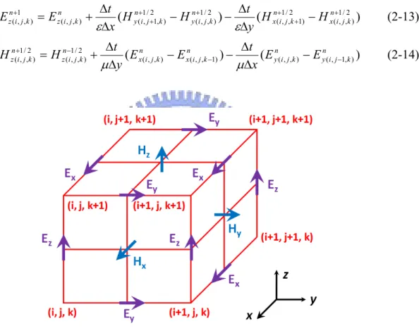
Since 1990’s, FDTD techniques have emerged as primary means to computationally model scientific and engineering problems dealing with electromagnetic wave interactions in various materials and structures, including PhCs. Comparing with PWE method, FDTD method is used to directly solve the time-dependent Maxwell's equations, the equations (2-3) and (2-4) in partial differential form. In Cartesian coordinates, these two equations can be derived as six scalar equations in (2-10), (2-11), and (2-12) [41]. The equations will be discretized using central-difference approximations to the space and time partial derivatives to obtain the dynamic behaviors of photon flow in PhC devices.
) ( 1 z H y H t Ex z y ∂ ∂ − ∂ ∂ = ∂ ∂ ε , ( ) 1 z E y E t Hx z y ∂ ∂ − ∂ ∂ = ∂ ∂ ε (2-10) ) ( 1 x H z H t Ey x z ∂ ∂ − ∂ ∂ = ∂ ∂ ε , ( ) 1 x E z E t Hy x z ∂ ∂ − ∂ ∂ = ∂ ∂ ε (2-11) ) ( 1 y H x H t Ez y x ∂ ∂ − ∂ ∂ = ∂ ∂ ε , ( ) 1 y E x E t Hz y x ∂ ∂ − ∂ ∂ = ∂ ∂ ε (2-12)
The basic FDTD space grid and time-stepping algorithm are proposed by Kane Yee in IEEE Transactions on Antennas and Propagation in 1966 [42]. In spatial domain, he proposed the vector components of the E- and H-field stagger spatially in rectangular unit cells of a Cartesian computational grid, which is named as “Yee cell” and shown in Fig. 2-1. In Yee cell, each E-field vector component is located midway between a pair of H-field vector components, and conversely.
On the other hand, in equation (2-4), the change in the E-field in time is dependent on the change in the H-field across space. Thus, in the simulation domain, the updated value of the E-field in time is dependent on the stored value of the E-field and the numerical curl of the local distribution of the H-field in space. The H-field is also in the similar time-stepping manner. Iterating the E- and H-field updates results in a marching-in-time process wherein
sampled-data analogs of the continuous electromagnetic waves under consideration propagate in a numerical grid stored in the computer memory. K. Yee proposed a leapfrog scheme for above marching-in-time progress as shown in Fig. 2-2. In Fig. 2-2, the E- and H-field updates are staggered in time domain sequentially. As a result, the E-field updates will be conducted midway during each time-step between successive H-field updates, and conversely. This process can be expressed as the following equations:
) ( ) ( 1/2 ) , , ( 2 / 1 ) 1 , , ( 2 / 1 ) , , ( 2 / 1 ) , 1 , ( ) , , ( 1 ) , , (+ + + + Δ + + − + Δ − − Δ Δ + = n k j i x n k j i x n k j i y n k j i y n k j i z n k j i z H H y t H H x t E E ε ε (2-13) ) ( ) ( (, , ) (, , 1) (, , ) (, 1, ) 2 / 1 ) , , ( 2 / 1 ) , , ( zni jk xni jk xni jk yni jk yni j k n k j i z E E x t E E y t H H + − − − − Δ Δ − − Δ Δ + = μ μ (2-14)
Fig. 2-2: Scheme of leapfrog time-stepping in FDTD algorism.
Another key issue in FDTD algorism is the boundary condition. To approximate an infinite domain to be a finite computational domain and save the computation time and computer memory, various boundary conditions are proposed, including Mur’s Boundary, perfectly matched layer, and absorbing boundary condition, which all eliminate the reflections when the wave impinge the boundary of the computational domain.
In summary, the resulting finite-difference equations are solved in a grid deviation in spatial domain and leapfrog manner in time domain. In the computations, the E-field components inside the Yee cell in space will be manipulated at a given instant in time domain. And then the H-field components in the same cell will be manipulated at the next instant in time domain. The process will be repeated until the desired electro-magnetic field behavior is fully evolved. Since it is a time-domain method, solutions can cover a wide frequency range with a single simulation run. In this dissertation, we will simulate and design the PhC-based devices based on above two methods by commercial software [39].
2-1-3 Simulation of Photonic Crystal Device
Based on above numerical methods, in this section, we calculate the photonic band diagram and the PBG effect of two-dimensional (2D) triangular PhC lattice shown in Fig.
Fig. 2-3: (a) Scheme of 2D triangular PhC lattice and (b) the corresponding PWE and FDTD simulated PBG effect.
2-3(a), which is composed by air holes on dielectric slab with infinite thickness. The indices of dielectric material and air hole are set to be 2.7 and 1.0. The lattice constant (a) and air hole radius (r) are set to be 500 and 150 nm, respectively. The calculated band diagram for transverse-electrical (TE) polarization is shown in Fig. 2-3(b). We can observe a large PBG region between the first (dielectric-band) and second (air-band) allowed photonic band. Besides, we can also directly simulate the optical wave (usually a plane wave or Gaussian dipole source in simulation) transmission through the PhC by FDTD method to locate the PBG region. The simulated transmission spectrum is shown in Fig. 2-3(b). In Fig. 2-3(b), the low transmission region indicates the PBG effect, which agrees with that performed by PWE method quite well. Although the FDTD method is much time-consumed than PWE method, this approach will be very promising in calculating PhC lattice structures cannot define the unit cell or be with very large unit cell, for example, the quasi-PhCs.
On the other hand, to investigate the designed PhC micro- and nano-cavities, the FDTD simulation will be applied very often to obtain the resonance spectrum, quality (Q) factor, effective mode volume, and so on. The Q factor is a very important parameter to evaluate the optical confinement ability of a microcavity. In FDTD simulations, there are two main approaches to evaluate the Q factors of resonance modes. The first one is directly recording
the energy decay rate of the resonance mode to evaluate the optical loss and calculate the Q factor by the following equation:
) 2 exp( ) ( Q t U t U o πω − = (2-15)
where ω denotes the resonance frequency. Obviously, for microcavity with ultra-high Q factor, the evaluation process needs great amount of time steps in FDTD simulation to obtain sufficient accuracy in exponential fitting, which is usually time-consuming and executed by cluster computations. The other approach evaluates Q factor by the resonance line width in frequency domain base on Padé approximation [43] and Fourier harmonic analysis, which provide a fast and better frequency resolution can be obtained without using longer simulation times.
Besides, the effective mode volume can be evaluated by the following equation [8]:
] ) ( ) ( max[ ) ( ) ( 2 3 2 r E r r d r E r V V eff ε ε
∫
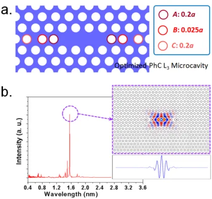
= (2-16)Here, we take optimized high Q PhC L3 microcavity [44] proposed by Prof. S. Noda’s
group for example, to verify the accuracy of the simulation tools we use. The scheme of optimized L3 microcavity design by three missing air holes is shown in Fig. 2-4(a). The
microcavity is optimized by shifting lattices A, B, and C with 0.2a, 0.025a, and 0.2a outward, respectively, as shown in Fig. 2-4(a). The lattice constant, r/a ratio, slab thickness and index are set to be 420 nm, 0.29, 240 nm, and 3.4, respectively, according to reference [44]. The simulated resonance spectrum and the main resonance mode profile in electrical field are shown in Fig. 2-4(b), which agree with the results in reference [44]. The Q factor and effective mode volume are calculated to be 2.3×10⁵ and 0.079 μm3, which also agree with
Fig. 2-4: (a) Scheme of optimized high Q PhC L3 microcavity. (b) 3D FDTD simulated
resonance spectrum and main resonance mode profile in electric field.
2.6×10⁵ and 0.071 μm3 in reference [44] quite well and verify the accuracy of the used simulation tools.
2-2 Nano-Fabrication of Two-Dimensional Photonic Crystal Cavities
The epitaxial structure of InGaAsP multi-quantum-wells (MQWs) for membrane structure is shown in Fig. 2-5. The epitaxial wafer consists of four 10 nm 0.85 % compressively-strained InGaAsP quantum wells which are separated by three 20 nm unstrained InGaAsP barrier layers. The summated thickness of MQWs is 220 nm, which is design for supporting single TE fundamental mode near wavelength of 1550 nm. It has been confirmed that the PL spectrum of the MQWs is centered at 1500 nm with 200 nm gain spectrum at room temperature, as shown in Fig. 2-5. The 60 nm InP capping layer is used to protect the MQWs during a series of dry etching processes.
Fig. 2-5: Designed epitaxial structure of InGaAsP MQWs, which is grown by Union Optronics Corporation, Taiwan. The PL spectrum centered near 1550 nm with 200 nm spectral span is also confirmed.
The nano-fabrication process of 2D PhC microcavity is illustrated as the following. First, the 140 nm silicon-nitride (Si3N4) layer served as hard mask for latter dry etching process is
deposited by plasma-enhanced chemical vapor deposition (PECVD) process. Then a 240 nm polymerthylmethacrylat (PMMA) layer is spin-coated on the Si3N4 layer. The PhC pattern is
defined on the PMMA layer by electron beam lithography technology (JSM-6500F, JEOL). After a series of development and fixation processes, the first mask for PhC pattern is prepared. The PhC pattern can be observed in scanning electron microscopy (SEM) picture shown in the inset A in Fig. 2-6. It is also worthy to note that we can gradually tune the PhC lattice cell size, that is, the air hole radius by choosing different point dosages during the electron-beam lithography process [45-47].
Second, for transferring the defined PhC pattern on PMMA mask into Si3N4 and InGaAsP
MQWs, the inductively coupled plasma / reactive ion etching (ICP / RIE) system (Plasmalab-100, Oxford Inc.) is used. The Si3N4 hard mask is etched by CHF3 / O2 mixed gas
in RIE mode, and then CH4 / Cl2 / H2 mixed gas is used to transfer the patterns into MQWs at
150 °C in ICP etching mode. The cross-section SEM pictures of etched PhC lattice on Si3N4
Fig. 2-6: The overview of the fabrication process of 2D PhC microcavity. The insets A to D show the SEM pictures of each PhC pattern transferring step during the fabrication process.
Third, to form the suspended slab structure, the InP substrate beneath the MQWs should be removed. The undercut can be achieved by using a mixture of HCl : H2O = 4 : 1 at 2 °C.
This process also removes the Si3N4 residue and the 60 nm InP capping layer and smoothes
the surface and the sidewall of the air holes. This process could be also regarded as a gentle wet etching process to reduce the scattering, i.e. optical loss, caused by the surface roughness [48]. The wet etching process is anisotropic. The wet etching stops at 95° and 40° from <-1, 0, 0> direction in the (0, -1, -1) and (0, 1, -1) planes, respectively [49]. The undercut trench under the PhC pattern can be formed for the larger air holes. For smaller air holes, the wet etching results in a small wedge-shape undercut in each air hole. The small wedges under every air hole have no chance to meet each other. As a result, no undercut trench can be formed. Thus, a window opening surrounds the device is applied to prevent the wet etching of the air holes from stopping. Then a 2D PhC suspended slab structure is completed, as shown in the inset D in Fig. 2-6.
2-3 Measurement Setup
2-3-1 Near-Infrared Micro-Photoluminescence System
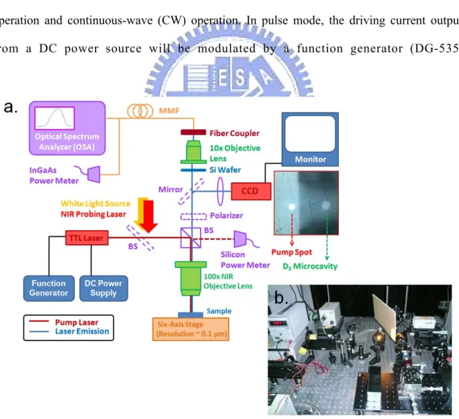
To characterize the epitaxial materials and various fabricated PhC micro- and nanocavities, a NIR confocal micro-PL system with sub-micrometer-scale resolution in microscope and sub-nanometer-scale resolution in spectrum is setup. The system configuration and photo of the micro-PL system are illustrated and shown in Fig. 2-7(a) and (b).
In this system, an 845 nm transistor-transistor logic (TTL) laser (APMT-60 ,Power Technology Inc.) is used as the pump source. This TTL laser can be operated both under pulse operation and continuous-wave (CW) operation. In pulse mode, the driving current output from a DC power source will be modulated by a function generator (DG-535,
Stanford Inc.), and then the laser light output will be under pulse operation. The pulse signal is generated by time-differential between two logic gate outputs and the pulse width of 200 fs can be achieved. However, the smallest achievable pulse width is limited to the summation of rise and fall time of the laser diode in TTL laser, which is about 19 ns. In CW operation case, the function generator is turned off and the internal circuit is short. In this case, the driving current will not be modulated and the laser output is in CW wave. Besides, the TTL laser output profile and beam divergence are shaped to a circle and collimated by its internal shaping module and mounted output collimator, respectively. These will be beneficial for the optical path alignment when setting up the system.
The TTL laser pump beam is split into two beams by a 50 / 50 beam splitter with 10 μm thickness (BP-150, Throlab. Inc.). One beam will be feed into a 100x long working distance NIR objective lens (M-Plan APO NIR series, Mitsutoyo Corp.) with numerical aperture of 0.42 mounted on a 3-axis stage. And then the pump beam is focused to a spot with 3 to 2.5 μm in diameter on the measured sample by the objective lens. The incident laser power on the sample will be estimated by detecting the other beam by a silicon power meter (1815-C, Newport Inc.), as shown in Fig. 2-7.
The simple microscopic function is also setup in this micro-PL system. By using a co-axial white light source and a charge-coupled device (CCD) camera, the sample mounted on a high resolution 3-axis stage can be observed from the monitor. A typical PhC D3
microcavity (formed by removing 19 missing air holes, cavity size ~ 2.6 μm in diameter) image captured by CCD camera is shown in the inset photo in Fig. 2-7(a). In this photo, the PhC microcavity laser can be observed clearly. One can see the positions of the microcavities and the 845 nm pump spot with 2.5 to 3 μm in diameter can be determined by comparing with the microcavity. By the 3-axis stage (561-series, Newport Inc.) with high resolution of 0.1 μm, the pump spot can be moved to the region we want to excite.
Fig. 2-8: The measured resonance spectrum from PhC D3 microcavity laser. The SEM picture
of Ph D3 microcavity is also shown in the inset.
of the sample. A silicon wafer is put after the beam splitter in order to block the reflected pump laser light. We use a 10x objective lens to feed the output signal into a FC / FC multimode fiber (MMF), and then detecting the signal by an optical spectrum analyzer (OSA) (AQ-6315A ,Ando Inc.) and an InGaAs power meter (Q8221, Advantest Inc.), respectively. The spectral resolution of the OSA is 0.05 nm and detection responsibility is from 350 to 1700 nm. By this NIR micro-PL system, the PL spectrum of the InGaAsP MQWs can be obtained, as shown in Fig. 2-5. Besides, we also measure a typical PhC D3 microcavity [50,
51] to verify the system setup. The measure resonance spectrum is shown in Fig. 2-8. The lasing peak is at 1595 nm and not shown in Fig. 2-8. The measured resonance peaks agree with the simulated mode in PhC D3 microcavity [50] quite well.
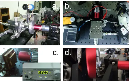
2-3-2 Systematic Accessories
For different purposes of measurement, we setup different system and sample stage accessories including substrate temperature controlling system for thermal behaviors investigation, current injection platform for electrically-driven devices, in-plane laser emission collection stage for waveguide-type laser devices, NIR tuning probe system for
Fig 2-9: Various sample stage accessories of NIR con-focal micro-PL system, including (a) gas detection chamber, (b) current injection platform, (c) substrate temperature controlling system, and (d) in-plane laser emission collection stage.
reconfigurable laser investigations, gas detection chamber for sensor device measurements, and so on. The photos of these accessories are shown in Fig. 2-9(a)-(d).
Among these accessories, the substrate temperature controlling system will be applied in Chapter 4 in this dissertation and the setup is illustrated as the following. We design a substrate temperature controlling system by clapping a thermo-electric cooler (TEC) between two copper slabs. The sample will be fixed on the top copper slab. Thus, we can control the sample substrate temperature by controlling the top copper slab temperature. In this system, a 10 kΩ thermistor with ± 0.01 °C accuracy is used to monitor the temperature of the top copper slab. The thermistor feedbacks data to the temperature controller (325-B, Newport Inc.) to decide the TEC driving current. A stable temperature will be achieved in 10 seconds.
2-4 Summary
In this chapter, at first, we introduce the theories of numerical methods for designing PhC devices, including PWE and FDTD methods. And then we illustrate our developed
nano-fabrication processes for fabricating PhC micro- and nano-cavity devices on InP-based semiconductor materials, which are composed by e-beam lithography technology, a series of dry- and wet-etching processes. We also setup a NIR con-focal micro-PL system with high spectral resolution and sensitivity to characterize the fabricated devices. And various systematic accessories for different measurements are also setup.
Chapter 3
8-Fold Quasi-Photonic Crystal Nanocavity & Circular Photonic Crystal
Microcavity with Whispering-Gallery Modes
In this chapter, at first, we briefly introduce the lattice structures and photonic band gap (PBG) effects of quasi-photonic crystals (QPhCs). And then we propose a D1 nanocavity
design with well-confined whispering-gallery (WG) mode based on 8-fold QPhCs under proper cavity modification. In experiments and simulations, including WG modal lasing actions, side mode reducing mechanism, and compact device size are investigated. In additions, we also investigate a novel circular-PhC (CPhC) lattice structure with isotropic PBG effect and apply it to construct a microcavity sustaining high quality (Q) WG mode.
3-1 Quasi-Photonic Crystals
Since the PhC nanocavity laser was firstly demonstrated by O. Painter et al. in 1999 [8], various attractive designs have been widely investigated as we mentioned in Chapter 1. With the PBG effect, well-controlled photon flows in PhC micro- and nano-cavities are extremely potential for quantum-electron dynamics (QED) devices and photonic integrated circuits (PICs) applications due to its ultra-high Q factor and ultra-low threshold. However, the anisotropy of PBG caused by the low-level symmetry in wave-vector (k) space has been found and investigated [52, 53]. Actually, higher-level symmetry can be obtained by the idea of quasi-periodic lattice comes from the solid-state physics and the anisotropy of PBG can be reduced. According to different symmetry level, various QPhC lattice structures have been proposed and demonstrated, for example, penrose (5-fold) [54], octagonal (8-fold) [55],
Fig. 3-1: Lattice structures of (a) penrose (5-fold), (b) octagonal (8-fold), and (c) dodecagonal (12-fold) QPhCs.
dodecagonal (12-fold) [56], and so on, as shown in Fig. 3-1. These lattice structures in spatial coordinates can be obtained by transforming specific periodic wave-vector arrangements in Fourier space [56].
In serving as the mirror of microcavity, the QPhCs would provide more efficient and uniform in-plane confinement in all directions due to the isotropic PBG effects [54, 56], which will be beneficial for achieving lasing properties with low threshold and high Q factor. Most importantly, various WG modes with high Q factors can be easily sustained in 2D micro- and nano-cavities based on different QPhCs. Very recently, various QPhC micro- and nano-cavity lasers have been investigated in theory and demonstrated in experiments by several groups [57-59].
3-2 8-Fold Quasi-Photonic Crystal Single-Defect Nanocavity
3-2-1 Cavity Design, Simulated, and Measured Modal Properties
In the beginning, we design a single defect nanocavity by removing a central air hole (named D1 nanocavity) based on 8-fold QPhC lattice as shown in Fig. 3-2(a). Then we
investigate the sustained defect modes in this nanocavity by three-dimensional (3D) finite-difference time-domain (FDTD) method. In the simulation setup, the slab thickness is 220 nm and the designed air-hole radius (r) over lattice constant (a) ratio is 0.3. From
![Fig. 1-2: Scheme of 2D PhC nanocavity firstly demonstrated by O. Painter et al. [8]](https://thumb-ap.123doks.com/thumbv2/9libinfo/8228797.170831/23.892.273.664.120.359/fig-scheme-d-phc-nanocavity-firstly-demonstrated-painter.webp)