國立交通大學
光電工程學系 顯示科技研究所
碩士論文
Ambipolar Phototransistors and Complementary-like
Inverters Based on Photosensitive Composite Films
利用複合半導體層製作雙極性感光電晶體
與類互補式反向器
研究生:鄭太獅
指導教授:陳方中 博士
利用複合半導體層製作雙極性感光電晶體
與類互補式反向器
Ambipolar Phototransistors and Complementary-like
inverters Based on Photosensitive Composite Films
研 究 生:鄭太獅 Student:Tai-Shih Cheng
指導教授:陳方中 博士 Advisor:Dr. Fang - Chung Chen
國 立 交 通 大 學
電機學院顯示科技研究所碩士班
碩 士 論 文
A Thesis
Submitted to Display Institute
College of Electrical and Computer Engineering
National Chiao Tung University
In Partial Fulfillment of the Requirements
For the Degree of Master
in
Display Institute
July 2008
Hsinchu, Taiwan, Republic of China
中華民國九十七年七月
利用複合半導體層製作雙極性感光電晶體
與類互補式反向器
碩士研究生:鄭太獅
指導教授:陳方中
國立交通大學顯示科技研究所碩士班
中文摘要
我們將 rr-P3HT 及 PCBM 以不同重量濃度比例混合於化學溶劑,並使用溶劑退火 方式塗佈形成電晶體之雙極性薄膜有機半導體層。觀察到當兩種材料在主動層中之比 例發生變化之同時,雙極性有機電晶體電性將同步展現電子及電動遷移率之消長變 化。此外,在實驗上進一步驗證各種接觸金屬與增添超薄金屬氧化層緩衝層對元件表 現之比較。本論文另一重點為發現研製之光電晶體在光照環境下將展現不同之電性調 變。最後,由於本實驗之半導體層乃 P 型及 N 型之混合層,實驗結果上發現較單一 P 型或 N 型半導體有較高之臨界電壓,是以固定 P3HT 並改以 PTCDI-C8 置換 PCBM 作上下 雙層結構,明顯的發現利用雙層結構能提升 P 型電子遷移率及顯著降低操作臨界電壓 同時也獲得較佳之 N 型特性。本研究乃詳盡地研究出以 P3HT 及 PCBM 之雙極性電晶體 特性並製作出基本反向邏輯電路,發現其光調變特性並對其光調變成因進行探討。半 導體材料物性則以原子力顯微鏡、X 光繞射儀、X 光光電子光譜儀及吸收光譜儀作輔助 分析。Ambipolar Phototransistor and Complementary-like
inverters Based on Photosensitive Composite Films
Student : Tai-Shih Cheng Advisor : Dr. Fang-Chung Chen
Department of Photonic and Display Institude
National Chiao Tung University
ABSTRACT
Various organic-semiconductor-based ambipolar transistors operated both in positive and negative gate voltage are recently key components in the field of organic complementary-like circuit development. Besides, it will be more potential by adopting solution-processed method or inject-printing methods. In the thesis, two famous organic conducting materials rr-P3HT and PCBM were introduced in developing photosensitive ambipolar field-effect transistors. Herein, we successfully make inverter circuit and let the characteristics discussed in this article. Besides, the variation of hole and electron mobilities are observed and got statistics according to different composite films of P3HT / PCBM ratio. Furthermore, we experimentally introduce different metal electrodes and ultra thin metal oxide layer for comparison to study the performances . In the thesis, another investigation is to fabricate phototransistor with variable characteristics under illumination and these characteristics may be the basis for developing phototransistor and the design of sensor circuit. To decrease the higher threshold voltage both in p-channel and n-channel, bi-layer structure and PTCDI-C8 were introduced to arrive the aim. After studying the characteristics of phototransistor based on the different composite films, we try to explain the mechanism of photoconductivity and photovoltaic effect under illumination. Finally, the semiconductor materials are analysed by AFM, XRD, XPS and UV-visible.
誌 謝
在這兩年的碩士研究生涯中,有幸接受陳方中及朱治偉兩位博士交叉指導, 無論是研究內容或是生活態度上的建議,都令我不斷省思且腦力激盪,僅以此文 獻給我由衷感謝的人。 首先,我要感謝指導教授陳方中博士。在研究生涯當中,您給了我珍貴的機 會到一流研究機構做研究,很遺憾自己剛開始自己花了很多時間摸索才上軌道, 感謝您在兩年中不斷導正學生實驗方向並給予明燈。此外,中央研究院朱治偉博 士親自指導我實驗中的技巧,使我得以突破研究上的困境,感謝朱老師提供我一 個相當優質的研究空間。 而兩位老師在對我做事情態度上的叮嚀更是深刻的教誨,讓我做實驗的時候 能夠事半功倍,相信我在這點滴過程中學到的歷練會成為將來我的生活中不可或 缺的一部分。 感謝川毅、孝慶、義凱學長在這兩年中將經驗及技巧毫不保留地傳授教導, 以及呈祥、昱仁、曉芬、家銘、淑萍、忠佑和俊威給予的相互思辨,每每都讓我 開拓了視界,改進再改進。另外特別要感謝應科所行政室怡君小姐在對我在實驗 設備上的培訓。 接著要感謝映頻學姐當初細心帶領,讓我能在短時間內掌握實驗室的狀況。 無論是實驗設備的完善或是人際關係間的和諧,讓我能夠喜歡這間充滿親切氣氛 的實驗室。 陪伴我兩年的所有伙伴,感謝大家在實驗上的配合、努力,以及相互間的扶 持協助,讓每個人都得以順利完成自己的研究生涯。還有大家在實驗問題上熱烈 的討論、遇到挫折時的勉勵、實驗成功時喜悅的分享,這些所有的點點滴滴都將 成為深刻的回憶。 實驗室的學弟妹,有你們的加入,才能使得實驗室有所傳承,感謝你們處理 實驗室的大小事務,讓我能心無旁騖地專心於自己的實驗上頭。特別是威寬及麗 芬在量測上的幫忙,誠摯地感謝你們的辛勞。Contents
中文摘要 ... i Abstract ... ii 誌謝... iii Contents ... iv List of Tables ... viFigure Captions... vii
Chapter 1 Introduction ...…1
1.1 Overview Organic Electronics...1
1.2 Overview Organic Ambipoalr Field-effect Transistors...3
1.3 Basic information about P3HT ... 4
1.4 Basic information about PCBM ... 6
1.5 Top Contact Structure of Field-Effect -Transistor... 7
1.6 Motivations ... 7
1.7 Thesis Organization ... 8
Chapter 2 Mechanism and Operation ... 9
2.1 The Charge Carrier Transportation in Organic Semiconductors ... 9
2.2 Hopping Model ... 10
2.3 Multiple Trapping and Release ( MTR )... 10
2.4 The Operation of Organic Field Effect Transistor... 11
2.5 The Parameters Extraction of Organic Thin Film Transistors ... 12
2.6 The Principle for the Operation of Complementary-like Inverter ... 14
Chapter 3 Experiment... 17
3.1 The Materials ... 17
3.2 The Device Fabrication ... 18
3.2.1 Substrates Preparation... 18
3.2.2 The Surface treatment of Gate/Active Layer Interface... 19
3.2.3 Spin Coating of P3HT/PCBM as the Active Layer... 19
3.2.4 Treat with Solvent Annealing and Thermal Annealing ... 19
3.2.5 Ultra Thin Metal Oxide MoO3 and V2O5 Deposited... 19
3.2.6 Evaporation Metal Electrode Onto Semiconductor Layer as the Electrode ... 20
3.3 The Device Measurement... 21
3.3.1 I-V Characteristics Measurement... 21
Chapter 4 Results and Discussion ... 23 4.1 Device Operated In N-Channel, Ambipolar , P-Channel ... 23 4.1.1 Output Characteristic of Ambipolar Field-effect Transistor ... 23 4.1.2 Transfer Characteristic of Ambipolar Field-effect
Transistor ... 24 4.1.3 Voltage Transfer Characteristic of Complementary-like
Inverter... 25 4.1.4 Dependence of Electron / Hole Mobilities on the Ratio of
the Composite Film... 30 4.1.5 Devices With Balanced Threshold Voltage ... 32 4.2 Device with Different Source-Drain Electrodes... 33
4.2.1 Device With Ca, Ag, Al and Au as Electrodes for
Comparison ... 33 4.2.2 Ultra-Thin Nano-Scale Transition Metal Oxide Layer ... 36 4.3 The Photoelectric Effect on the Ambipolar Device ... 40 4.4 The Morphologic Analysis With Different P3HT and PCBM
Composition ... 47 4.5 The GIXRD Diagram of the Different Composite Films... 50 4.6 Bi-layer Ambipolar Field-Effect Transistor Based on
PTCDI-C8 and P3HT... 53 Chapter 5 Conclusions ... 57 References ... 59
List of Tables
Table 2-1 Transistor ”Switch model” ... 16 Table 4-1 The Parameters of Different Concentrations ... 31 Table 4-2 Mobilities and the Factor K of Ambipolar OFETs with Different
Electrode... 33 Table 4-3 The Electrical Parameters of Ambipolar OFETs with Different
Electrode... 36 Table 4-4 The Electrical Parameters of Ambipolar OFETs with Ultra-Thin
Nano-Scale Transition Metal Oxide Layer ... 39 Table 4-5 Shifted Threshold Voltage toward Positive Gate Voltage vs
different ratio P3HT:PCBM under illumination ( AM1.5G ) ... 44 Table 4-6 The Electrical Parameters of Bi-layer Ambipolar Field-effect
Figure Captions
Fig. 1-1 In 1983, the TFTwas made by polyacetylene and polysiloxane[2] 2 Fig. 1-2 The evolution of organic electronics [6] ……….…2 Fig. 1-3 The chemical structure of the P3HT [22] ………. 4 Fig. 1-4 (a) 2D conjugated P3HT lamellae (b) nanowire-like structures
form by self-organization [23]………5 Fig.1-5 Orientations of P3HT on the substrate (a) P3HT lamellae normal to substrate (b) P3HT lamellae parallel to substrate [24]…….…...5 Fig. 1-6 The chemical structure of [6,6]-phenyl-C61-butyric acid methyl
ester[25-26]……….6 Fig. 1-7 Out-of-plane XRD patterns of spin-coated PCBM films. Insets
show AFM images of PCBM films .[27] ………..…….6 Fig. 1-8 The field effect transistor structures Top contact………. ..7 Fig. 2-1 Electron states (a),(b): localized states (c): delocalized states
[28]……… …9 Fig. 2-2 Charge carrier hopping ...……….10
Fig. 2-3 Operation of a)p-type and b)n-type OFET ………11 Fig. 2-4 ID-VD output characteristics plot of the p-type transistor……… 12
Fig. 2-5 ID-VG transfer characteristics plot of the p-type transistor……. 13
Fig. 2-6 ID-VG transfer characteristics plot of the ambipolar transistor…14
Fig. 2-7 Vout-Vin transfer characteristics plot of the ambipolar FET……. 15
Fig. 3-1 The structure of materials that used in experiments……….17 Fig. 3-2 The flow chart of experimental procedure………20 Fig. 3-3 Schematic configuration of the O-CMOS inverter in a) top view
and b) cross section……….. 21 Fig. 3-4 A schematic of an atomic force microscope………22 Fig. 4-1 Output characteristic of ambipolar field-effect transistor in p-type a) and n-type b) conduction……….23 Fig. 4-2 Transfer characteristic of ambipolar field-effect transistor in p-
Fig. 4-3 Structure of Complementary-like ambipolar inverter ……….. 25 Fig. 4-4 Transfer characteristics of complementary-like ambipolar
inverter in the a)first and b)third quadrants with their corresponding gains ………... 26
Fig. 4-5 Voltage Transfer characteristic of Complementary-like
ambipolar inverter operating at voltages of 60–80 V………... 27 Fig. 4-6 Output Gain of Complementary-like ambipolar inverter
operating at voltages of 60–80 V ……….… 27
Fig. 4-7 Hysteresis in Voltage Transfer characteristic of inverter….…. 28 Fig. 4-8 Hysteresis of Transfer characteristic in a) p- and b) n-type
conduction for ambipolar OFET …..……… 29
Fig. 4-9 Dependence of the electron and the hole mobilities on the ratio of the composite film in organic transistors at room temperature ………...30
Fig. 4-10 The threshold voltage of p- and n-channel in ambipolar FETs.32 Fig. 4-11 Energy level diagrams of P3HT and PCBM in contact with Ca, Al, Ag and Au without any applied bias between source, drain and gate contacts ………..33
Fig. 4-12 The relationship between the ratio of ambipolar transport and the work functions of different source and drain electrodes…34 Fig. 4-13 Sputter depth profile of Al/ MoO3 thin film using C60
sputtering ………37
Fig. 4-14 X-ray Photoelectron Spectrometry (XPS) spectra of a) O 1s and b) Mo 3d ………...37
Fig. 4-15 (a) A schematic cross-section configuration of our top-contact layer of OFETs. (b) Energy band diagram in equivalent of
( P3HT+PCBM)/ MoO3/Al and ( P3HT+PCBM)/Al………38
Fig. 4-16 The output a) and transfer b) characteristics of the singleP3HT transistor measured in the dark and under illumination(AM 1.5G) ……….40
Fig. 4-17 The output a) and transfer b) characteristics of the single PCBM transistor measured in the dark and under
illumination(AM 1.5G) ……….….40
Fig. 4-18 The simple physical model for illustration of mobile charges separated in organic films after the absorption of photons. The “-“ and “+” symbols represent mobile electrons and holes, respectively ………..41
Fig. 4-19 The output characteristics of the ambipolar transistors measured in the dark and under illumination……….. .42 Fig. 4-20 The transfer a) and transfer b) characteristics of the ambipolar transistors measured in the dark and under illumination .43
Fig. 4-21 Shifted Threshold Voltage Vs different weight ratio
P3HT:PCBM under illumination AM1.5G ………45
Fig. 4-22 (a)The Normalized UV–Vis absorption spectra for P3HT:PCBM composite films for different amount.(b) reference spectra for AM1.5G(IEC 60904) and Oriel Snlight simulator machine[32] ………46
Fig. 4-23 The Morphologic Analyses with different P3HT and PCBM composition………49 Fig. 4-24 The GIXRD diffraction of the different P3HT and PCBM
composition (a)10:0(b)4:1(c)2:1(d)1:2(e)0:10the intensity is in the logarithmic scale ………52
Fig. 4-25 The output a) and transfer characteristics b) of bbii--llaayyeerr a
ammbbiippoollaarr ffiieelldd--eeffffeecctt ttrraannssiissttoorr bbaasseedd oonn PPTTCCDDII--CC88 ((2200nnmm)) a
annddPP33HHTT((2200nnmm)) ……………………………………………………………………………………………………5544
Fig. 4-26 The output a) and transfer characteristics b) of bbii--llaayyeerr a
ammbbiippoollaarr ffiieelldd--eeffffeecctt ttrraannssiissttoorr bbaasseedd oonn PPTTCCDDII--CC88 ((5500nnmm)) a
Chapter 1
Introduction
1.1 Overview Organic Electronics
The organic electronics have been widely applied to various aspects [1], such as organic light-emitting diodes (OLEDs), organic solar cells, organic thin-film transistors (OTFTs) etc.
The advantages are basically as followings: (1) Solution processibility
(2) Low-temperature processibility (3) Light-weight.
The disadvantages of are basically as followings: (1) Unstable
(2) Lower mobility.
In 1983, F, Ebisawa et al. announced the polyacetylene and polysiloxane to be the active layer and the dielectrics of OTFTs. [2] The electrical transfer characteristics is shown in Fig.1-1 .The field-effect mobility was on the order of 10-5 cm2/Vs. Later, new materials like polythiophene were discovered. [3] However, the mobility was still low. Then the poly(3-hexylthiophene) was used to be the active layer in TFT by A. Assadi et al. in 1988. [4] The pentacene devices has been reported in 1992. [5] The mobility is about 2x10⁻³ cm2/Vs. Recently, the most popular organic materials used in OTFTs is pentacene.Fig.1-2 shows the evolution of organic thin-film transistors. In 2000, the mobility of pentacene has surpassed that of the amorphous silicon.
Fig. 1-1 In 1983, the TFT was made by polyacetylene and polysiloxane [2]
1.2 Overview Organic Ambipoalr Field-effect Transistors
“Plastic transistors” open the future of flexible displays, smart cards, radio frequency identification tags, Progress in this field has been made improving the material properties and the process techniques rapidly.
Recently, organic field-effect transistors (OFETs) has been extensively studied for their use in large-area and low cost applications, such as displays, smart cards and radio frequency identification tags [7-10]. Inverters are the basic elements for complex integrated circuits. OFETs with ambipolar transport are desirable for complementary technology because of their ease in fabrication and circuit design. There are several configurations to achieve ambipolar OFETs such as bilayers [11-13], bulk heterojunction [14-15]and single-component materials [16-20]. In particular, bulk heterojuction configuration which blends p- and n-type organic semicondutors to form the active layer simplified the fabrication process, while maintaining the attractiveness of easy solution process.
Herein, the ambipolar OFETs based on composite films of regioregular poly(3-hexylthiophene) (rr-P3HT) and [6,6]-phenyl-C61-butyric methyl ester (PCBM) were
1.3 Basic information about P3HT
Poly(3-hexylthiophene), P3HT, is a conjugate polymer and is used as the active layer of organic thin-film transistors. Four carbon atoms and one sulfur atom compose a thiophene. The thiophene is the main chain structure of the P3HT. The side chain of P3HT is a hexyl group. Depending on the position of the alkyl chain to the main chain, there are two different regioregularities: head-to-tail and head-to-head, respectively. Fig. 1-3 shows the chemical structure of the P3HT and the different structure between the head-to-tail and the head-to-head.
Fig. 1-3 The chemical structure of the P3HT [22]
According to the research of H. Sirringhaus et al., in solution processes, the self-organization of conjugated polymers forms ordered microstructures, in which these micro-size domains are embedded in an amorphous matrix. In P3HT, the self-organization can result in lamellaes with two-dimensional conjugated sheets formed by interchain stacking as shown in Fig. 1-4 (a) [23]. The two-dimensional conjugated sheets may form a narowire-like structures (Fig. 1-4 (b)) when strong self-organization process occurs. As the P3HT was spin-coated on the substrate, the lamellae of P3HT have two orientations related to the substrate: normal and parallel to the substrate. Fig. 1-5 illustrates the two different orientations of P3HT. [24]
Fig. 1-4 (a) 2D conjugated P3HT lamellae (b) nanowire-like structures form by self-organization [23]
Fig. 1-5 Orientations of P3HT on the substrate (a) P3HT lamellae normal to substrate (b) P3HT lamellae parallel to substrate [24]
The P3HT is a semiconducting material. Because of the overlaps of the electron orbitals, the energies of excitation states and the steady states of π electrons split into the highest occupied molecular orbital (HOMO) and the lowest unoccupied molecular orbital (LUMO). The HOMO and the LUMO are a concept that is similar to the energy band in inorganic semiconductors. However, the HOMO is analog to the valence band and the LUMO is analog to the conduction band. The HOMO of P3HT is between -4.8 and -5.2 eV and the LUMO of P3HT is about from -2.7 to -3.0 eV according to different literature. The band gap of P3HT is about 2.0 eV.
(a) (b)
(a) (b)
1.4 Basic information about PCBM
It have been reported that solution- processed [6,6]-phenyl C61-butyric acid methyl ester (PCBM),shows high field-effect electron mobility 0.004–0.01 cm2/V s. [25-26] And its structure is showed in Fig 1-6. The HOMO of PCBM is about -6.1 eV and the LUMO of PCBM is about -4.2 eV according to different literature. The band gap of PCBM is about 2.0 eV.
Fig. 1-6 The chemical structure of [6,6]-phenyl-C61-butyric acid methyl ester[25-26]
Besides, no diffraction peak was observed in the PCBM film from the XRD measurement in FIG. 1-7. The AFM image of the PCBM film demonstrates a homogeneous morphology without large crystalline domains FIG. 1-7.These results indicate that the PCBM film takes an amorphous-like structure or is composed of homogeneously distributed small nanocrystals. These findings agree with the results of transmission electron microscopy observation and electron diffraction measurement of spin-coated PCBM film reported by Yang et al.[27]
Fig. 1-7 Out-of-plane XRD patterns of spin-coated PCBM films. Insets show AFM images of PCBM films .[27]
1.5 Top Contact Structure of Field-Effect Transistors
According to the position of source-drain electrode, organic field-effect transistors (FET) are divided into two structures: top contact and bottom-contact. In Fig. 1-8, the advantage of top contact structures is that there is a smaller contact resistance between the active layer and electrodes and the performance is better generally. But the channel length defined by the shadow mask can hardly decrease. The FETs with top contact structures has relative high off current because the back channel current flow near the source drain electrode.
Fig. 1-8 The field effect transistor structures Top contact
1.6 Motivations
Polymer field-effect transistors (FETs) show promise as the critical components for low-cost, flexible electronics with various applications. And it is reasonable for us to adopt the organic material P3HT and PCBM which have better solubility for solution-process step.
These applications typically require complementary logic elements, which require both p-type and n-type transistors. However, it is beneficial to utilize “ambipolar” FETs, which
function both as p-channel and n-channel transistors by using the composite film of P3HT and PCBM. Therefore, it is our important aim to practice ambipolar complementary field-effect transistors inverters in this thesis.
blends consisting of P3HT and PCBM by varing the composition ratio. Furthermore, the correlation between the contact metal and work function needed to be realized clearly. Since P3HT and PCBM were studied in detail in organic solarcells, the condition for solvent annealing and proper thermal annealing may exist the condition for optimization and is needed to consider in OFET . Finally, because the FETs based on photosensitive composite films, we want to check how the device can tune its electrical characteristic under illumination. And the mechanism of photoelectric effect are tried to observed and explained.
1.7 Thesis Organization
This thesis is organized as following. In this chapter, the background of this study is described briefly:
Chapter 1 introduces the background knowledge of materials and FFT structures
Chapter 2 explains the mechanism of the charge transportation in organic materials and the method of the parameter extraction in this article.
Chapter 3 describes the experiments and the measurement instruments used in this study.
Chapter 4 describes the results of characteristics from measurement. Finally, chapter 5 gives the conclusions of our experiments.
Chapter 2
Mechanism and Operation
2.1 The Charge Carrier Transportation in Organic Semiconductors
The interaction between molecules in organic materials is van der Waals force. The van der Waals force is relative weaker than the covalent bonding between the atoms in inorganic materials. Hence the charge carrier transportation is quite different between organic and inorganic materials.
The π-bonding electron cloud has two states: localized states and delocalized states. The π-bonding electron is localized if the electron bound to particular atom. The localized π-bonding electron can not contribute to the carrier transportation. Fig. 2-1 shows the π-bonding electron states of benzene.
Fig. 2-1 π electron states (a),(b): localized states (c): delocalized states [28] Generally, there are two models to describe the delocalized electrons transportation in organic materials, hopping model [29] and multiple trapping and release model (MTR) [30]
2.2 Hopping Model
In organic materials, the intermolecular transportation of charge carrier depends on hopping as shown in Fig.2-2. This is the limitation of the charge carrier mobility in organic materials. Because the phonons would assist the hopping of carriers, the mobility increases with the increasing temperature. The relation between the mobility of the hopping and the temperature can be described as the following equation:
1/ 0exp[ ( / ) ]T T0
α
μ μ= −
where the α is ranged from 1 to 4.
Fig.2-2 Charge carrier hopping
2.3 Multiple Trapping and Release (MTR)
The MTR model is widely used in a-Si semiconductors. In MTR model, it assumes that there exist localized levels in the band gap due to defects. These localized levels are like traps for charge carriers. These levels would form a narrow band with high concentration of trap levels. When the charge carriers transport to the levels, the carriers would be trapped with the probability near 100%. On the other hand, the activation energy of the carrier determines the release of the carrier. The released carrier would contribute to the transportation and the drift mobility is given as following:
0 exp( / )
D E kTt
μ =μ α −
where Et is the energy level of the defects, α is the ratio between the density of states
2.4 The Operation of Organic Field Effect Transistor
The organic thin-film transistors are operated in accumulation mode. When the gate biases a negative voltage, the holes would accumulate in the interface between the active layer and the insulator. If there are enough holes to accumulate in the interface, the channel is formed and the transistor is in ON state. When the drain is biased at a negative voltage, the drain current would flow from the source to the drain. The concept is also the same for a n-type OFET while the gate biases a positive voltage, the electrons would accumulate in the interface between the active layer and the insulator.
Fig. 2-3 illustrates the operation of the (a) p-type and (b) n-type organic transistors.
Fig. 2-3 Operation of a)p-type and b)n-type OFET
The transistor is a three-terminal device. There are two transfer characteristics plots. The first plot is ID-VD characteristics as shown in Fig. 2-4. The ID versus VD relation is
measured under several constant VG. The transfer characteristics are separate into two
regimes. The linear regime occurs when VD approaches to zero. The transistor behaves as a
resistance. When VD is increasing, the transistor would be in the saturation regime. In
saturation regime, the ID is governed by VG.. The second plot is ID-VG transfer
characteristics as shown in Fig. 2-5. From the ID-VG plot, many parameters like the mobility
and threshold voltage can be extracted.
2.5 The Parameters Extraction of Organic Thin Film Transistors
Although the transportation mechanism in organic materials is different from that of inorganic materials, the transfer characteristics are similar. The formula derived from the inorganic semiconductors was adopted to calculate the parameters like the field-effect mobility and threshold voltage in this article.
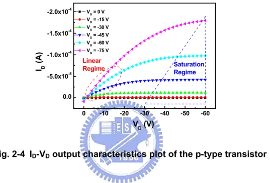
0 -10 -20 -30 -40 -50 -60 0.0 -5.0x10⁻⁵ -1.0x10⁻⁴ -1.5x10⁻⁴ -2.0x10⁻⁴ Saturation Regime I D (A) VD (V) VG = 0 V VG = -15 V VG = -30 V VG = -45 V VG = -60 V VG = -75 V Linear Regime
Fig. 2-4 ID-VD output characteristics plot of the p-type transistor
The typical p-type ID-VD transfer characteristics is shown Fig. 2-4. When the TFT is
operated at linear regime, the drain current is governed by the equation 2-1.
D D T G i D
V
V
V
V
L
WC
I
)
2
(
−
−
=
μ
(2-1)where W is the channel width in cm, L is the channel length in cm, Ci is the
capacitance per unit area in F/cm2, μ is the field-effect mobility in cm2/Vs, the Vt is the
threshold voltage in Volt.
When VD>VG-VT, the TFT is operated at saturation regime. The drain current is given
by the equation 2-2. 2 ) ( 2 G T D V V L WCi I =
μ
− (2-2)μ
L
WC
V
I
i const V G D D2
)
|
|
(
=
∂
∂
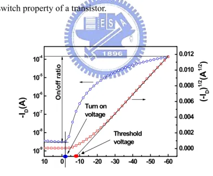
= (2-3)The slope can be obtained from the ID-VG transfer characteristics plot shown in Fig.
2-5. The fitting line of the square root of ID in ID1/2-VG plot in the saturation regime, the
intersect of the line and the x-axis is the VT. The turn on voltage Von and the on/off ratio can
be obtained form the ID-VG transfer characteristics plot.
The subthreshold swing is a parameter to determine the switch speed of a transistor. It can be calculated by equation 2-4.
]
)
|)
log(|
[(
.
1 const V G D DV
I
Min
Swing
S
− =∂
∂
=
(2-4)The dimension of subthreshold swing is V/decade. The subthreshold swing gives the degree of the switch property of a transistor.
10-9 10-8 10-7 10-6 10-5 10-4 10 0 -10 -20 -30 -40 -50 -60 0.000 0.002 0.004 0.006 0.008 0.010 0.012 Turn on voltage On/off ra ti o (-I D ) 1/ 2 (A 1/ 2 ) -I D (A ) Threshold voltage
2.6 The Principle for the Operation of Complementary-like Inverter
Complementary metal–oxide–semiconductor (CMOS) is a major class of integrated circuits used in digital logic circuits and for a wide variety of analog circuits such as image sensors, data converters, and highly integrated transceivers for many types of communication. A CMOS inverter contains a PMOS and a NMOS transistor connected at the drain and gate terminals, a supply voltage VDD at the PMOS source terminal, and a
ground connected at the NMOS source terminal, were VIN is connected to the gate terminals
and VOUT is connected to the drain terminals. It is important to notice that the CMOS does
not contain any resistors. Two important characteristics of CMOS devices are high noise immunity and low static power consumption. Significant power is only drawn when the transistors in the CMOS device are switching between on and off states.
Three potentials in the model would simply be VG, VD, and VS. We use the
source/drain-symmetric model to show that two ambipolar transistors with the same gate voltage connected in parallel, as shown in Fig.2-6 , behave as a NMOS and a PMOS transistor with twice the channel current of either single device for any combination of VG,
VS, and VD. Ambipolar OFET Ambipolar OFET VDD Vss Vout Vin Ambipolar OFET Ambipolar OFET VDD Vss Vout Vin
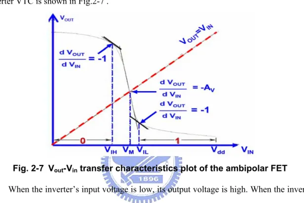
The static characteristics of an inverter are usually described by a voltage transfer characteristic (VTC), which is sometimes also called a DC transfer characteristic. The VTC
is essentially a plot of the inverter’s output voltage as a function of its input voltage. A typical inverter VTC is shown in Fig.2-7 .
Fig. 2-7 Vout-Vin transfer characteristics plot of the ambipolar FET
When the inverter’s input voltage is low, its output voltage is high. When the inverter’s input voltage is high, it’s output voltage is low. For each input voltage, we define an incremental voltage gain of the inverter as the slope of the VTC at that point. The incremental
voltage gain basically tells us by how much the output voltage will change for a given small change in the input voltage at any point along the curve. Note that the VTC has a negative slope everywhere, which implies that the inverter’s output voltage decreases as its input voltage increases and vice versa. The VTC has three distinct regions: two in which the curve is relatively flat and one in which the curve is quite steep. We normally operate the inverter in one of the two flat parts of the curve when we use it as a logic gate.
By keeping the inverter biased in the steep part of the VTC, we can also use it to linearly amplify small signals. The logic high (VIH) and low (VIL) threshold voltages are
considered to be logical 0s and input voltages above VIH are considered to be logical 1s. The
range of input voltages between VIL and VIH is called the transition region. The point in the
transition region where the inverter’s input voltage is equal to its output voltage is called the transition threshold (VM). The incremental gain of the inverter attains its maximum value at
the transition threshold, so we would like to operate the inverter at or near this point when using it as an amplifier.
The general shape of the VTC of the inverter is critical to the reliable operation of digital circuits. Because the magnitude of slope of the VTC is less than unity on the ends of the VTC (i.e., in the logic high and low parts of the curve) and it is larger than unity in the transition region, the inverter has two very important properties that make digital circuits robust.
In essence, an inverter can take a weak 0 and turn it into a strong 1 or it can take a weak 1 and turn it into a strong 0. We simply could not build digital circuits with many stages of processing if it weren’t for this restoring property.
In Table 2-1,the switch model of the traditional MOSFET transistor is defined as follows:
Table 2-1 Transistor "switch model"
MOSFET Condition on MOSFET State of MOSFET
NMOS Vgs<Vtn OFF
NMOS Vgs>Vtn ON
PMOS Vsg<Vtp OFF
PMOS Vsg>Vtp ON
When VIN is low, the NMOS is "off", while the PMOS stays "on": instantly charging V to
logic high. When Vin is high, the NMOS is "on and the PMOS is "on: draining the voltage at V to logic low.
Chapter 3
Experiments
3.1 The Materials
The head-to-tail regioregular poly(3-hexylthiophene) (or as called HT rr-P3HT) bought from Rieke Metals.Inc。and [6,6]-phenyl-C61-butyric methyl ester (PCBM)
which is shown in Fig. 3-1(a) (b) were used in the composite active layer of organic ambipolar field-effect transistors. We dissolved the P3HT and PCBM in the chlorobenzene (CB) . In order to make better ambipolar OFET, PTCDI-C8 is the candidate to replace the PCBM and serves as the role to study the OFET with bi-layer structure. Besides, wafers with 200 nm SiO2 deposited , calcium, aluminum, gold, silver ,Molybdenum oxide
(MoO3 :Sigma-Aldrich, 99.99% purity) are used in experiment.
The chemical structures of materials mentioned are shown in Fig. 3-1.
Fig. 3-1 The structure of materials that used in experiments. (d)
(b)
(c) (a)
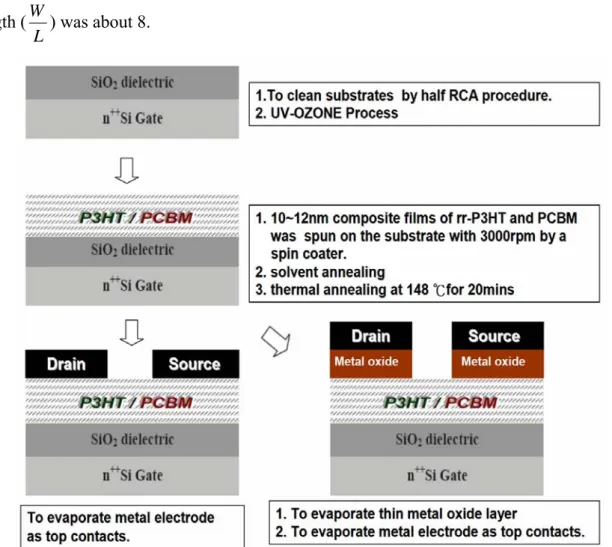
3.2 The Device Fabrication
As the wafers were prepared, fig. 3-2 show the flow chart of experimental procedure and the devices were fabricated in N2-filled environment
by following steps:
1. The surface treatment of the gate/active layer interface. 2. To spin coat the P3HT and PCBM as the active layer. 3. To treat the devices with the solvent annealing. 4. To treat the devices with the thermal annealing.
5. To evaporate wide bandgap material as buffer layer only in special cases . 6. To evaporate metal electrode as the electrode.
3.2.1 Substrates Preparation
The substrates were heavily doped n-type highly silicon wafers and resistance was about 0.001~0.003 ohm-cm. The conductance of the wafers is high enough to serve as the gate electrode. By using thermal growth, about 200 nm SiO2 deposited on the wafers is as
the gate insulator. The measured capacitance per unit area is about 14.1 nF/cm2.Our substrates are rinse with DI (de-ionized) water for 5 minute to remove large particles. And then the substrates are rinsed with the mixture of H2SO4 and H2O2 for 15 minute. The mixed
ratio is H2SO4:H2O2=3:1. H2SO4 and H2O2 are strong oxidant and capable of removing
chemical substances. To remove the residual mixture H2SO4 and H2O2, the wafers are rinsed
with DI water for 5 minute. Finally, the nitrogen gun is uesd to blow our wafers to remove the residual water in sequence. After the first steps of RCA cleaning, the wafers are placed into an hot plate which the temperature is set to 110℃ for over 30 mins to remove the crystal water. After cleaning the substrate, the substrate was also processed with the UV/ozone dry-cleaning technology .
3.2.2 The Surface Treatment of the Gate/Active Layer Interface
Generally , the defects between the interface of inorganic material and the organic material come from the different surface properties. Before the deposition of the active layer, the surface of the wafers are treated with UV-ozone for 15 minute to increase –OH groups on the wafers and the organic material in some cases.
3.2.3 Spin Coating of the P3HT/PCBM As the Active Layer
The rr-P3HT was obtained from the Rieke Metals and the PCBM was obtained from the Rieke Metals, Inc. The composite films of active layer of P3HT and PCBM were spin coated on the surface-treated substrate in the glove box which filled with nitrogen. The spin rate was set to 3000 rpm for 60 seconds to obtain uniform films.
3.2.4 Treat with Solvent Annealing and Thermal Annealing
In spite of high spin rate, there was still some solvent left on the device . To controll the evaporation rate of the residual solvent to be slower than usual . The device is placed in a smaller oven and then the evaporation rate can decrease in saturation solvent vapor pressure .All devices were placed in small Petri dishes until the residual solution dried for 30mins.For our OFETs, the proper annealing temperature is an important factor to optimize The Electrical characterization of ambipolar OFET. After solvent annealing, we placed devices on a 148℃ pre-heated hotplate for 20 minutes. Then all devices were placed in a room temperature environment to cool down.
3.2.5 Ultra Thin Metal oxide MoO3 Deposited
Since the MoO3 are wide band-gap materials . Thus, they can serve as buffer layer
3.2.6 Evaporation Metal Electrode on Semiconductor Layer as the Electrodes After the composite film of P3HT-PCBM employed as the active layer, different metals Ca, Al, Ag and Au should be chosen as the main electrode by thermal evaporation to form the source and drain electrodes called top-contact structure in the N2-filled glove box. It was sublimated by thermal coater under a back pressure below 2×10⁻³ Pa. As for deposition rate, it was controlled at a rate of 2.0~2.5 Å/sec by a quartz oscillator during the electrode formation until the total thickness approached 50 nm. However, the channel length and width of the OFETs used were 25μm and 2mm. The ratio of channel width over channel length (
L W
) was about 8.
3.3 The Device Measurement
3.3.1 I-V Characteristics Measurement
Electrical characterization was both measured in dark and under illumination for comparison. Herein, all the devices were also measured by semiconductor parametric analyzer HP 4156C in the N2-filled glove box. For P3HT-PCBM based devices, a negative bias of gate voltage was applied to accumulate holes in the p-type active layer while a positive bias of gate voltage was applied to accumulate electrons in the n-type active layer. In the ID-VD
measurement of p-channel, the drain bias was swept from +10 to -100 Volts and the gate voltage step were 0, -15, -30, -45, -60, -75, -90 Volts, respectively. In the ID-VG measurement,
the gate bias ranged from 0 to -90 Volts, and the drain voltage step were 0, -15, -30, -45, -60,-75,-90 Volts. On the same way, the measurement for ID-VD and ID-VG in n-channel was
also performed Finally, electrical characterization was measured in under illumination AM 1.5G illumination with intensity of 100 mW/cm2 for comparison.
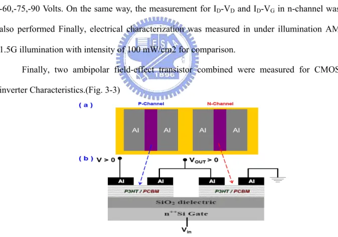
Finally, two ambipolar field-effect transistor combined were measured for CMOS inverter Characteristics.(Fig. 3-3)
Fig. 3-3 Schematic configuration of the O-CMOS inverter in a) top view and b)
cross section. For both p and n channels, the ratio of channel width over
channel length (
L W
3.3.2 Surface Morphology Measurement
We used the tapping-mode atomic force microscope (AFM) to obtain the surface morphology of the active layer. By the interaction of the van der Waals force between the tip of the cantilever and the surface topology of the sample, the cantilever vibrates due to the magnitude of the interaction. Detecting a laser beam reflected by the cantilever can sense the tiny vibration of the cantilever. The computer record these detected signals and construct the surface morphology of samples. Fig. 3-4 illustrates the structure of AFM. From the surface morphology, we have clues to realize the relation between the device performance and the morphology of the active layer.
Fig.3-4 A schematic of an atomic force microscope
While a tapping-mode AFM measuring, the probe oscillates up and down regularly. It prevents the probe to damage the surface of the samples and obtains extra information about the samples. The computer records the feedback amplitude and the phase signals of the cantilever. From the amplitude signals we can obtain the morphology information. The phase signals reveal the different materials or structures of the sample.
Chapter 4
Results and Discussions
4.1 Device Operated in N-Channel , Ambipolar, P-channel
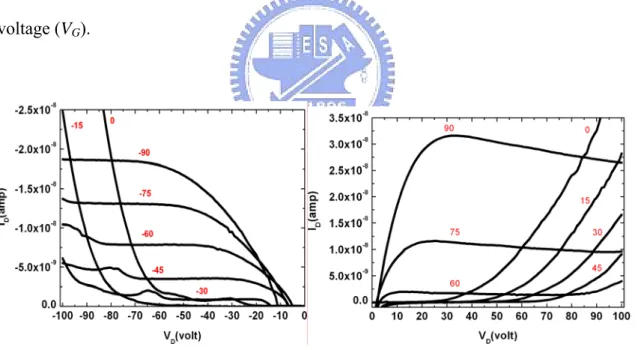
4.1.1 Output Characteristic of Ambipolar Field-Effect Transistor
The drain-source current (IDS) vs. drain-source voltage (VDS) characteristics of an
ambipolar OFET using SiO2 as the dielectric at different gate voltages (VG) are shown. In Fig.
4-1(a)(b), The device showed apparent ambipolar operations. The output characteristics displayed very good, clear saturation currents which behaved as a function of the gate bias voltage (VG).
Fig. 4-1 Output characteristic of ambipolar field-effect transistor in p-type a) and n-type b) conduction. (composition ratio of P3HT:PCBM = 2:1)
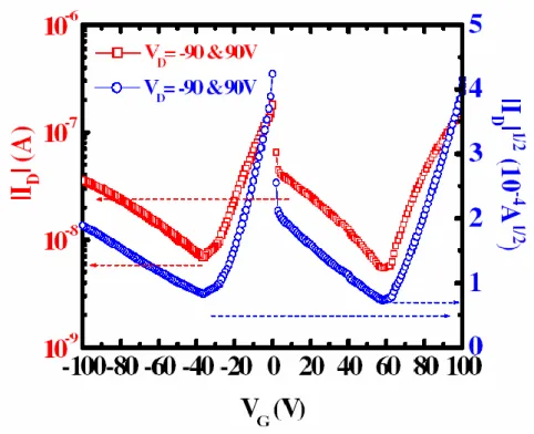
4.1.2 Transfer Characteristic of Ambipolar Field-Effect Transistor
In Fig. 4-2, Strong field-effect modulations of the channel conductance in ambipolar operations were observed, with threshold voltage (VT) of -40 and 58 for p- and n-type
behavior. The mobility of holes and electrons were 7.5×10⁻⁵ and 2.1×10⁻⁴ cm2/V-s, respectively.
Fig. 4-2 Transfer characteristic of ambipolar field-effect transistor in p- and n-type conduction. (composition ratio of P3HT:PCBM = 2:1)
4.1.3 Voltage Transfer Characteristic of Complementary-like Inverter
The gates of the N- and P-channel FETs are connected in fig. 4-3 , and they serve as an input node (Vin). The drains of the two FETs are also connected, and they serve as an output node (Vout). The source of the N-channel FET is grounded, while the source of the P-channel FET is connected to a power supply (VDD > 0), where VDD= 80 V was applied. The
drain currents, IDn and IDp, for the PCBM (N-channel) and P3HT (P-channel) thin-film FETs
were measured as a function of Vout, where the drain-source voltage for the N-channel FET,VDS, and the source-drain voltage of P-channel FET respectively. The plot of Vout-Vin
measured directly in the circuit is shown in Fig 4-4. and the threshold voltage of this circuit, VTIC, is 50 V. Inverter switching characteristics are clearly seen in the range of 60–80 V in fig 4-5 and fig 4-6.
Ambipolar OFET Ambipolar OFET VDD Vss Vout Vin Ambipolar OFET Ambipolar OFET VDD Vss Vout Vin
Fig. 4-3
Structure of Complementary-like ambipolar inverter
We have fabricated a CMOS logic NOT circuit composed of two ambipolar FETs serves as an N-channel FET and a P-channel FET. The structure of CMOS inverter circuit is shown in Fig.4-3 . Transfer curve for three regions ,noise margin and logic swing as following summary from Fig 4.4
(a):1. Low level input voltages region :VIN < 44V.
2. Transition region: 44V< VIN <63V
Noise Margin : NMH= VOH- VIN =(100-60)V=40V NML= VOH- VIN =(45-20)=25V 0 1 0 2 0 3 0 4 0 5 0 6 0 7 0 8 0 9 0 1 0 0 0 1 0 2 0 3 0 4 0 5 0 6 0 7 0 8 0 9 0 2 1 0 -1 -2 -3 -4 -5 -6 -7 -8 V OUT (V) VD D= 8 0 V Gain VIN (V ) G a in = 7 .3 9 -1 0 0 -9 0 -8 0 -7 0 -6 0 -5 0 -4 0 -3 0 -2 0 -1 0 0 -9 0 -8 0 -7 0 -6 0 -5 0 -4 0 -3 0 -2 0 -1 0 0 0 -1 -2 -3 -4 -5 -6 V OU T (V) VD D=-80V Gain VIN (V ) G ain = 5.90
Fig. 4-4 Transfer characteristics of complementary-like ambipolar inverter in the
a) first and b) third quadrants with their corresponding gains. (composition
ratio of P3HT:PCBM = 2:1)
( a )
0 10 20 30 40 50 60 70 80 90 100 0 10 20 30 40 50 60 70 80 V OUT (V ) VIN(V) VD D=80 V VD D=60 V
Fig. 4-5 Voltage Transfer characteristic of Complementary-like ambipolar inverter operating at voltages of 60–80 V
Fig. 4-6 Output Gain of Complementary-like ambipolar inverter operating at voltages of 60–80 V
Since inverter are the basic building block of most of the logic circuits, we fabricated inverters, by integrating two ambipolar transistors. They are capable of operating in first and third quadrants. When the supply voltage (VDD) and input node (VIN) are biased positively, the
inverter works in first quadrant with the maximum voltage gain of 7.39 in Fig.4-4(a) .Meanwhile, when the supply voltage (VDD) and input node (VIN) are biased
negatively, the inverter works in third quadrant with the maximum voltage gain of 5.90 in Fig.4-4(b).Complementary-like inverters connected with two identical ambipolar FETs are able to operate with gains around 6~8 . Therefore, the ambipolar FETs are shown to be promising candidates in organic electronic applications. However, Fig. 4-7 shows that hysteresis in voltage transfer characteristic of inverter measured by retrace mode. This is because the ambipolar transistor has a hysteresis in the current characteristic of ambipolar OFET in fig 4-8 . 0 10 20 30 40 50 60 70 80 90 100 0 10 20 30 40 50 60 70 80 90 -2 -1 0 1 2 3 4 5 6 7 8 9 10 V OUT (V ) VDD = 80 V | Gai n| V IN (V) Gain = 7.39
Fig.4-8 Hysteresis of Transfer characteristic in a) p- and b) n-type conduction for ambipolar OFET
4.1.4 Dependence of Electron / Hole Mobilities on the Ratio of the Composite films
Fig. 4-9 shows the hole and electron mobilties of the ambipolar devices made with different P3HT and PCBM composition. The Table 4-1 also shows that dependence of the electron and the hole mobilities on the ratio (P3HT/ P3HT+PCBM) of the composite film in organic transistors at room temperature in N2-filled environment. The concentration of the P3HT solution was held at 0.5 wt% and PCBM was 0.5 wt%, 0.25 wt%,0.125 wt%, 0.055wt% and 0wt% respectively. Obviously, both hole and electron mobilities were significantly lower than that of the corresponding unipolar devices. Herein, Fig. 4-9 illustrates that the devices can be operated in three different modes: n-channel (region I), ambipolar (region II) and p-channel (region III). The graph also indicate that the hole and electron mobility exist in equal balance at the ratio of P3HT/ P3HT+PCBM about the range between 0.67 ~ 0.75 . Table 4-1 shows the electrical parameters of device with aluminum electrode and different weight ratio.
Fig. 4-9 Dependence of the electron and the hole mobilities on the ratio of the composite film in organic transistors at room temperature .The dash lines are guidances to the eyes. Field-effect mobilities based on single component P3HT (1.0 ) and PCBM (0 ) transistors are also shown in the graph.
Table 4-1 The electrical parameters of different concentrations P3HT:PCBM P3HT concentratio n (wt%) PCBM concentration (wt%) P3HT P3HT+PCBM Hole Mobility (cm2/Vs) Electron Mobility (cm2/Vs) 1:1 0.5 0.5 1.8×10⁻⁵ 2.5×10⁻³ 2:1 0.25 0.67 7.8×10⁻⁵ 2.6×10⁻⁴ 3:1 0.167 0.75 2.2×10⁻⁴ 6.5×10⁻⁵ 4:1 0.125 0.8 2.1×10⁻⁴ 9.3×10⁻⁵ 9:1 0.5 0.055 0.9 2.3×10⁻⁴ 4.9×10⁻⁶ 10:0 0.5 0 1 8.1×10⁻⁴ 0 0:10 0 0.5 0 0 1.1×10⁻³ P3HT:PCBM P-channel On/Off ratio N-channel On/Off ratio P-channel Vth (V) N-channel Vth (V) 1:1 1.1×10² 1.3×10² -41 52 2:1 3.1×10² 2.4×10² -42 55 3:1 3.1×10² 5.1×10² -44 50 4:1 1.0×10² 2.5×10² -43 52 9:1 5 1.7×10³ -30 87
4.1.5 Devices with Balanced Threshold Voltage
In an ambipolar OFETs, it has been found that hole and electron mobilities significantly decrease with the mixing of P3HT and PCBM from those of pure materials. Fig. 4-10 shows the threshold voltages (Vth) of both p- and n-channel in an organic ambipolar FET made at different pre-annealing temperatures. One can found that the Vth strongly depends on the pre-annealing temperature. It can be also noted that the slope of increasing n-channel Vth is close to the one of decreasing p-channel Vth on negative voltage bias. Therefore, the higher pre-annealing temperature, 160 ℃ , can improve p-channel Vth. In contrast, the lower pre-annealing temperature 140℃ is rather suitable for n-channel. However, the difference of |Vth| between p- and n-channel conduction devices is an important factor for complementary-like inverters. Based on the results, the optimized pre-annealing temperature is located at the range between 140 ℃ to 150 ℃ for inverters. Therefore, the pre-annealing temperature 148℃ is chosen as the primary condition for following experiments.
Fig. 4.10 The threshold voltage of p- and n-channel in ambipolar FETs (composition ratio of P3HT:PCBM = 2:1)
4.2 Devices made with different Source-Drain Electrodes
4.2.1 Devices made with Ca, Ag, Al and Au as Electrodes for comparison
In order to further understand the existence of the ambipolar behavior, four different metal electrodes, Ca, Ag, Al, and Au, were used as the S/D contact to vary the barrier height for hole and electron injection into the P3HT and PCBM, respectively. Energy band diagram of P3HT and PCBM and the work functions of different metals are shown in Fig. 4-11.
Fig. 4-11 Energy level diagrams of P3HT and PCBM in contact with Ca, Al, Ag and Au without any applied bias between source, drain and gate contacts.
All these devices showed ambipolar characteristics as well. The summary of ambipolar OFETs with different metals as S/D electrodes is given in Table 4-2 and Table 4-3.
Table 4-2. Mobilities and the factor K of ambipolar OFETs with different electrodes.
The result indicated that the work function of metals has to be considered to match the composite of the active layer. Further, an empirical factor, K, which stands for the ratio of electron mobility and hole mobility, is defined (Fig. 4-12). K decreased increasing work function. In other words, the calcium electrode, which has a lower work function is more suitable for electron injection. On the contrary, the gold electrode, which has a higher work function leads to a balanced mobility as K = 1.3. It is probably due to the fact that PCBM has higher intrinsic mobility. The results here suggest that the source and drain electrodes have profound effect on the performance of ambipolar devices. Table 4-3. shows the electrical parameters of ambipolar OFETs with different electrodes.
Fig. 4-12 The relationship between the ratio of ambipolar transport and the work functions of different source and drain electrodes.
Ca Ag Al Au 1.0 1.5 2.0 2.5 3.0 3.5 4.0 4.5 5.0 5.5 E lect ron M ob ili ty H o le M o b ili ty
Factor k= Electron Mobility Hole Mobility
Table 4-3 The Electrical parameters of ambipolar OFETs with different electrodes. Ambipolar FET Operated in N-channel Electron Mobility (cm2/Vs) P-channel Vth (V) P-channel On/Off ratio Electrode Al P3HT:PCBM=2:1 2.5×10⁻⁴ -45 2.4×10² Electrode Ag P3HT:PCBM=2:1 8.8×10⁻⁴ -42 1.3×10² Electrode Au P3HT:PCBM=2:1 8.2×10⁻⁴ -43 1.8×101 Electrode Ca P3HT:PCBM=2:1 5.6×10⁻⁴ -55 1.3×101 Ambipolar FET Operated in P-channel Hole Mobility (cm2/Vs) N-channel Vth (V) N-channel On/Off ratio Electrode Al P3HT:PCBM=2:1 7.4×10⁻⁵ 55 3.2×10² Electrode Ag P3HT:PCBM=2:1 1.9×10⁻⁴ 56 2.1×10² Electrode Au P3HT:PCBM=2:1 6.3×10⁻⁴ 54 1.0×101 Electrode Ca P3HT:PCBM=2:1 1.1×10⁻⁵ 47 1.1×10²
4.2.2 Ultra-Thin Nano-Scale Transition Metal Oxide Layer Between the Electrode / Organic interface
Bi-layer source-drain S-D electrodes for ambipolar OFETs are demonstrated. The bilayer consists of a transition metal oxide MoO3 layer and a metal layer. The ultra-thin nano-scale layer serves as the charge-injection layer by directly contacting the organic semiconducting layer. Herein, in order to realize the composition of ultrathin nanoscale MoO3 film, X-ray Photoelectron Spectrometry (XPS) is introducing to analyze the chemical composition and elemental state.
As shown in Fig. 4-13, utilizing a combination of C60+ and Ar+ beam sputtering, the mixed sputtering successfully sputter the MoO3 film through the bottom glass substrate.
According to the XPS spectra, the increasing or decreasing tendency of the composition elements can be apparently observed. It is observed that the composition of Al exhibited gradually decreasing and that of Mo and O exhibited abruptly increasing at about 20 min sputtering time in Fig. 4-13. Besides, it is also easy to realize that the film of MoO3 composed
of MoO4 (Mo4+,228ev) and MoO3(Mo6+, 231ev) indicates its doping effect from the binding
energy analysis(Fig.4-14(a)(b)). However, the effect of doping can help the promotion of conduction.
Fig. 4-13 Sputter depth profile of Al/ MoO3 thin film using C60 sputtering.
Fig. 4-14 X-ray Photoelectron Spectrometry (XPS) spectra of a) O 1s and b) Mo 3d. 524 528 532 536 540 5000 10000 15000 20000 25000 30000
(a)
O 1sBinding energy (eV)
In te ns it y ( a .u ) 224 228 232 236 240 0 4000 8000 12000 16000 20000 MoO3 MoO2
(b)
Mo 3d3/2 Mo 3d5/2 Intensity (a.u)Binding energy (eV)
20 40 60 80 0 2000 4000 6000 8000 10000 12000 14000 16000 O 1s A l2p M o3d M o3p3 M o4p M o3s
Intensity (a.u)
In this section, we report an effective way to enhance hole and electron transport in ambipolar field-effect transistors (FETs) by inserting an ultra-thin nano-scale molybdenum oxide (MoO3 ) layer at the electrode/organic interface to form a bi-functional source/drain
(S/D) electrode. It can be observed that the presence of ultra-thin nano-scale molybdenum oxide layer will facilitate the injection of holes from source/drain electrodes to organic semiconductor, resulting in a significant enhancement of the p-channel conduction without seriously sacrificing n-channel conduction. This achievement can be attributed to the discontinuous molybdenum oxide islands in Fig. 4-15(a), which can decrease the energy barrier of source/drain electrode Al for hole injection and permit the underlying metal electrode to contact with organic semiconductor for electron injection in Fig 4-15(b).
Fig. 4-15 (a) A schematic cross-section configuration of our top-contact layer of OFETs. (b) Energy band diagram in equivalent of ( P3HT+PCBM)/ MoO3/Al and
( P3HT+PCBM)/Al.
Utilizing the discontinuous islands as an interlayer is an effective and easy method to fabricate high performance. This results in the formation of two different junctions at metal/organic semiconductor interface, which are (P3HT+PCBM)/ MoO3/Al and
( P3HT+PCBM)/Al. Therefore, the ultra thin MoO3 layer makes better hole injections for the
ambipolar FETs.
Devices with the bilayer S-D electrodes showed enhanced hole-injection and electron-injection compared to those with only metal electrode. High field-effect mobility and
lower threshold voltage were obtained in the case by using the bilayer S-D electrodes at a gate bias of −90 and 90 V in Table 4-4. The improvement is attributed to the reduction in the contact barrier and the prevention of metal diffusion into the organic layer and/or unfavorable chemical reaction between the organic layer and the metal electrode.
Table 4-4. The Electrical parameters of ambipolar OFETs with Ultra-thin
nano-scale transition metal oxide layer
Hole Mobility (cm2/Vs) Electron Mobility (cm2/Vs) P-Channel Switch On Voltage (V) N-Channel Switch On Voltage (V) Electrode Al P3HT:PCBM=2:1 1.32×10⁻⁴ 4.7×10⁻⁴ -38 53 Electrode Al
1nm metal oxide MoO3 P3HT:PCBM=2:1
2.9×10⁻⁴ 4.9×10⁻⁴ -20 57
Based on the discussion above, doped transition metal oxide MoO3 decomposed into
MoO4 ( Mo4+)and MoO3 ( Mo6+) forming the extremely discontinuous nanoscale film.
Reviewing the performance of device, we also found that the doped ultra-thin nano-scale layer coupled between composite film and metal layers played an important role in improving field-effect transistor characteristics of ambipolar OFETs.
4.3 The photoelectric effect on the ambipolar device
Before studying the photoelectric effect on the ambipolar device, it is necessary to understand the output and transfer characteristics of the single P3HT and single PCBM transistors measured in the dark and under illumination in Fig 4-16(a)(b) and Fig4-17(a)(b) .
The curve shifted positively and p-channel threshold voltage decreased 10 V under illumination. In contrast, the threshold voltage shifts only 1V in n-channel is also observed.
0 -20 -40 -60 -80 -100 0.0 1.0x10⁻⁴ 2.0x10⁻⁴ 3.0x10⁻⁴ 4.0x10⁻⁴ 5.0x10⁻⁴ 6.0x10⁻⁴ 7.0x10⁻⁴ 8.0x10⁻⁴ 9.0x10⁻⁴ Shift Vth=10 Vth(in Dark)= -17 Vth(under illumination)= -7 -60 -90 -60 -90 |ID | 1/2 (A 1/ 2 ) VG(Volt)
Fig 4-16 The output a) and transfer b) characteristics of the single P3HT transistor measured in the dark and under 100mW/cm2illumination(AM 1.5G).
0 10 20 30 40 50 60 70 80 0.0 5.0x10⁻⁵ 1.0x10⁻⁴ 1.5x10⁻⁴ 2.0x10⁻⁴ 2.5x10⁻⁴ 3.0x10⁻⁴ 3.5x10⁻⁴ -60 -60 Shift Vth=1 Vth(in Dark)= 18 Vth(under illumination)= 17 |ID | 1/ 2 (10 -3 A 1/ 2 ) VG(volt)
Fig 4-17 The output a) and transfer b) characteristics of the single PCBM transistor measured in the dark and under 100mW/cm2 illumination(AM 1.5G).
The ultrafast photo-induced charge transfer between P3HT and PCBM has been extensively studied and has been applied to fabricate organic solar cells. The enhance photocurrent can be explained as the simple model shown in Figure 4-18.
Fig. 4-18The simple physical model for illustration of mobile charges separated in organic films after the absorption of photons. The “-“ and “+” symbols represent mobile electrons and holes, respectively.
The photoelectric effect on the device is also further studied in the ambipolar devices. The curves of drain-source current (IDS) vs. drain-source voltage (VDS) of ambipolar OFETs at
different gate voltages (VG) in dark and under illumination are shown in Figure 4-19. The IDS
increases both on positive or negative biases. When either P3HT or PCBM absorbs photons, holes and electrons are separated and accumulated between the source and drain electrodes. As a result, the channel opens itself by accumulating the photo-induced electrons and holes without any external applied bias between source, drain and gate electrodes. Therefore, the larger photocurrent can be reasonably observed at the same gate bias.
Fig 4-19 The output characteristics of the ambipolar transistors measured in the dark and under illumination. The composition ratio is P3HT:PCBM = 2:1.
Figure 4-20(a)(b) further shows the transfer characteristics of the ambipolar FET both under illumination and in the dark. The curve shifted positively and p-channel threshold voltage decreased. In contrast, the higher threshold voltage in n-channel is also observed.
-1 0 0 -8 0 -6 0 -4 0 -2 0 0 2 0 4 0 6 0 8 0 1 0 0 1 0-1 1 1 x 1 0-1 0 1 x 1 0-9 1 x 1 0-8 1 x 1 0-7 1 x 1 0-6 1 x 1 0-5 VD= -9 0 & 9 0 V in S u n lig h t VD= -9 0 & 9 0 V log 10 |I D | VG (V )
Fig 4-20The output a) and transfer b) characteristics of the ambipolar
transistors measured in the dark and under illumination. The composition ratio is P3HT:PCBM = 2:1.
(a)
Since p- and n-channels will interfere with each other because of the recombination effect in ambipolar transportation, the experimental formula equation derived can be express as:
p-type: |V
so (100mW/cm 2)
|=| V
so(In Dark)|- |V
SD(additional bias)| (4-1)
n-type: |V
so (100mW/cm2)|= |V
so(In Dark )|
+|V
SD(additional bias)| (4-2)
Herein, the relationship can also be checked from the formula |VDS(sat) |=|VGGS| - |Vth |in S
saturation region(Fig 4-20(a)). It is found that lower VDS(sat) in n-channel and higher VDS(sat) in
p-channel under illumination. Thus, the ambipolar OFETs based on P3HT-PCBM (2:1 ratio) with changeable characteristics under illumination can be regarded as a photoFET component and applied to the design of photodetector circuit.
However, Table 4-5 and Fig 4-21shows the Shifted Threshold Voltage with different weight ratio of P3HT and PCBM under illumination (AM 1.5G) .
Table 4-5 Shifted Threshold Voltage toward positive gate voltage Vs different ratio P3HT:PCBM under 100mW/cm2 illumination ( AM 1.5G )
Weight Ratio of P3HT:PCBM
P-Channel Mode N-Channel Mode
10:0 10 - 9:1 10~11 19~20 4:1 10~11 13 3:1 9~11 9~11 2:1 9~11 9~11 1:1 5~6 4~5 0:10 - 1
Fig 4-21Shifted Threshold Voltage Vs different weight ratio P3HT:PCBM under illumination AM1.5G .
In order to explain the shifted threshold voltage showed in Fig 4-21, we observed that the absorption spectra of thin films obtained by spin-coating a blend of P3HT:PCBM from solution showed a significant blue-shift when the amount of PCBM is 67 wt.% or more (1:2 wt. ratio of P3HT:PCBM), resulting in reduced red part absorption. Chirvase et al. [31] have reported similar trend in the absorption spectra modification and have attributed this change to destruction of ordering in the P3HT chains in the presence of PCBM. From our experiments, we demonstrate that the absorption spectra modification in P3HT:PCBM composite films is due to two possible interactions: first, the destruction of ordering of P3HT chains, as suggested earlier by Chirvase et al. [31], and second, due to a non-photoinduced charge transfer between P3HT and PCBM.
Fig. 4-22 shows the UV–Vis absorption spectra measured for P3HT from film and solution and for P3HT:PCBM films, for different wt. ratios of the two components. The absorption of the films with increasing amount of PCBM reduced significantly in the visible range, specifically between 450 and 600 nm which is the peak absorption wavelength band for P3HT. The peak absorption wavelength and the maximum absorption intensity changed
![Fig. 1-1 In 1983, the TFT was made by polyacetylene and polysiloxane [2]](https://thumb-ap.123doks.com/thumbv2/9libinfo/8252533.171759/13.892.230.692.114.422/fig-tft-polyacetylene-polysiloxane.webp)
![Fig. 1-5 Orientations of P3HT on the substrate (a) P3HT lamellae normal to substrate (b) P3HT lamellae parallel to substrate [24]](https://thumb-ap.123doks.com/thumbv2/9libinfo/8252533.171759/16.892.140.761.382.704/orientations-substrate-lamellae-normal-substrate-lamellae-parallel-substrate.webp)
![Fig. 2-1 π electron states (a),(b): localized states (c): delocalized states [28] Generally, there are two models to describe the delocalized electrons transportation in organic materials, hopping model [29] and multiple trapping and release model (MTR)](https://thumb-ap.123doks.com/thumbv2/9libinfo/8252533.171759/20.892.132.787.524.884/localized-delocalized-generally-delocalized-electrons-transportation-materials-trapping.webp)