Journal of Alloys and Compounds 481 (2009) 270–273
Contents lists available atScienceDirect
Journal of Alloys and Compounds
j o u r n a l h o m e p a g e :w w w . e l s e v i e r . c o m / l o c a t e / j a l l c o mNovel morphology and solidification behavior of eutectic bismuth–tin
(Bi–Sn) nanowires
Shih Hsun Chen
a, Chien Chon Chen
b,∗, Chuen Guang Chao
aaDepartment of Materials Science and Engineering, National Chiao Tung University, Hsinchu 30050, Taiwan bDepartment of Energy and Resources, National United University, 1, Lienda, Miaoli 36003, Taiwan
a r t i c l e i n f o
Article history:Received 14 February 2009
Received in revised form 17 March 2009 Accepted 18 March 2009
Available online 27 March 2009 Keywords: Bi–Sn nanowires Eutectic AAO Stoichiometry Solidification
a b s t r a c t
In the present work we show a simple and robust fabrication process for dense and continuous bismuth–tin (Bi–Sn) eutectic nanowires. The Bi–Sn eutectic nanowires of 200 nm diameter and several tens ofm in length were fabricated by a vacuum hydraulic force method. The alloy melt was injected into an anodic aluminum oxide (AAO) template to form nanowires after melt solidification. For this pro-cess, nanowires were formed from non-atomic deposition with liquid alloy; in this way, the composition of nanowires can be controlled precisely in stoichiometry. The Bi–Sn melt was restricted inside the AAO which has a low thermo-conduction and long period cooling rate around the melt. On the other hand, the heat flow is along the tube Z-axis and the melt is solidified from the AAO bottom to top because of the open pore on the AAO top. The eutectic nanowires were found to be dense and continuous with a uniform diameter throughout the length of the wires and with a lamellar microstructure along the wires’
Z-axis. In addition, the alternative segmental compositions showed that the ratio of tin to bismuth is
approximately 3.3:1.
© 2009 Elsevier B.V. All rights reserved.
1. Introduction
Solid metallic nanowire is a one-dimension material. It has been exploited for a wide range of applications that take advantage of their large aspect ratio (length/diameter). Recently, fabricating nanowires by atomic deposition or non-lithographic methods are emphasized in literature[1–5]. The atomic deposition methods such as, electrodeposition[6], metalorganic vapor-phase epitaxy [7], thermal evaporation[8–10], thermal decomposition[11], phys-ical vapor deposition (PVD)[12], and chemical vapor deposition (CVD)[13]are famous for nanowires fabrication. However, there are some problems with nanowires formed from atomic deposition. For example, the high cost of instrumentation; low efficiency of form-ing nanowires; conditions must be controlled carefully; difficulty in controlling the nanowires’ composition in the stoichiometry; dif-ficulty in making alloy nanowires; and the catalyst always reduces the purity of nanowires. Metal casting has been used in indus-try for several decades, and the casting technics have also been developed well. Therefore, combining the traditional process with nano-technology is helpful for cutting down the cost of nanowire fabrication.
∗ Corresponding author. Tel.: +886 37 381836; fax: +886 37 381237. E-mail address:[email protected](C.C. Chen).
Understanding the solidification behavior and the formation of alloys can help us to recognize the mechanical properties of cast products and to gain the expected properties through particular processes. Since the 1940s, much effort has been con-sistently invested in establishing this fundamental knowledge [14,15]. As the development of industry progressed toward semi-conductors, such basic research was not suspended; on the contrary, it extends even to the solders and the issue of lead toxicity[16–22]. Seeking substitute solders made of various ele-ments for specific purposes continued another research trend [23,24].
Among those substitution materials for Pb-based solders, the eutectic Bi43–Sn57 alloy was regarded as one with high poten-tial for use in fuse products and low temperature applications. Bi43–Sn57 alloy also exhibits some more advantages[25–27]apart from low temperature; therefore, the Bi–Sn system has always been an important topic no matter whether in solid or liquid phase from the 1940s to the present. Reviewing the literature, most investi-gations have referred to its macro-properties or the procedures of bulk Bi–Sn alloy, and only a small number were focused on submicron- or nano-scaled behaviors or theories. Here, we utilized a template-assisted method[28]to fabricate the eutectic Bi43–Sn57 alloy nanowire, which might retain more characteristics of bulk material than those common Bottom-Up processes; as expected an unusual and novel microstructure was observed. This phenomenon differs greatly from bulk eutectic Bi–Sn alloy; thus, a model of the
0925-8388/$ – see front matter © 2009 Elsevier B.V. All rights reserved. doi:10.1016/j.jallcom.2009.03.107
S.H. Chen et al. / Journal of Alloys and Compounds 481 (2009) 270–273 271
Fig. 1. Phase diagram of solidification of an alloy with equilibrium at the liquid–solid
interface[32].
solidification process is cited to explain how the development of the microstructure occurred.
To describe the crystal structure of an alloy, we might look back upon the solidification processes to clarify its causes. The most con-venient approach to the understanding of solidification phenomena is to consider them in terms of the macroscopic properties of mate-rials, such as temperature, latent heat, composition, and surface free energy, and to consider their influences separately[29–31]. Most engineering alloys solidify over a range of temperature rather than at a discrete melting point. Therefore, a uniform liquid alloy under a constant cooling rate could just be thought of as the effect caused by the fractional variation in composition through the entire process of solidification.
Solidification of most substances from their melt is closely approximated by the assumption of equilibrium at the interface during growth. That is, there may be large concentration gradients in the solid and liquid during solidification and the transporting barrier of atoms across the interface must be negligible. When solid-ification is occurring at temperature T, the condition of equilibrium at the interface defines the liquid and solid compositions at the interface CLand CS.Fig. 1shows the phase diagram of solidifica-tion of an alloy with equilibrium at the interface. In addisolidifica-tion, the equilibrium distribution coefficient, K, is defined as[32]:
K = CS CL
(1) In most particular cases, the solute distribution within the solid is assumed and no diffusion occurs. Another critical assumption under a rapid solidification process is that diffusion is limited in the liquid and there is no convection. For these two factors, the composition profile can be redrawn asFig. 2.
Here, we report the fabrication of Sn-Bi alloy nanowire by a die-casting process. Nanowires of alloy were fabricated using a hydraulic force process. The nanowires were formed from melt of alloy, directly. The composition of nanowires is controlled. Addi-tionally, in terms of instrumentation, it is cheaper than atomic deposition. Also, nanowires with well-defined morphology and high surface area were fabricated and the microstructures were discussed.
2. Experimental procedures
The eutectic bismuth–tin (Bi–Sn) nanowires used for this study were synthe-sized by a template-assisted vacuum hydraulic pressure injection process; for more details about that apparatus, refer to the literature from our laboratory[28]. Firstly,
Fig. 2. Composition profile in solidification with no diffusion in the solid and limited
diffusion and no convection in the liquid.
Bi–Sn eutectic bulk alloy was prepared using the vacuum melting method. The anodic aluminum oxide (AAO) with an average pore diameter of 220 nm, which was fabricated by means of anodizing aluminum foil in phosphoric acid, served as the mold for the injection procedure. Then, we removed the ceramic template, and the nano-structured Bi–Sn eutectic alloy was produced.
The characteristics of Bi–Sn nanowires were examined by scanning electron microscopy (SEM, JEOL 6500F FESEM and FEI Quanta 600 FESEM), energy disper-sive spectroscopy (EDS), transmission electron microscopy (TEM, JEOL 2010), and scanning TEM (STEM, FEI Tecnai G2F20). Standards of 6H SiC single-crystal lattice
fringes[33]and a cross-line grating replica were used to calibrate the TEM/STEM images.
3. Results and discussion
A bulk Bi–Sn material of eutectic stoichiometric composition was fabricated by a vacuum smelting process. The examinations revealed its characteristic melting point of 139◦C and the lamel-lar microstructure, as shown inFig. 3. In our tests, we confirmed the properties of the alloy, which include its compositions, melt-ing point and crystalline, then injected it into the AAO template to synthesize nano-scaled Bi–Sn eutectic wires. Through a
dissolu-Fig. 3. Typical OM image of cast bulk Bi–Sn eutectic material with a lamellar
272 S.H. Chen et al. / Journal of Alloys and Compounds 481 (2009) 270–273
Fig. 4. High-resolution back-scattered SEM images of a Bi–Sn eutectic nanowire
bundle.
tion process, the AAO was removed by using a 6 wt% chromic acid solution at 60◦C; after that, the eutectic Bi–Sn nanowires could be obtained. From morphology images of the Bi–Sn nanowire bun-dle, a segmented appearance is observed. InFig. 4, the further high-resolution back-scattered SEM images (BEI) reveal a global segmented structure. A TEM was utilized to analyze what caused this variation. Fig. 5 shows the TEM morphology and mapping images of the nano-wires bundle. According to the mapping infor-mation, the banded appearance resulted from distinct chemical compositions. In addition, the Bi segment occupied a shorter frac-tion and the Sn a relatively longer one. This sequence of eutectic microstructure along its growth direction is different from the typical Bi–Sn eutectic, which is arranged perpendicularly to the liquid–solid interface.
The fact that the interlamellar interface was approximately nor-mal compared to the mean solid–liquid interface could be explained through the solidification behavior of bulk eutectic alloys, which was shown experimentally by Straumanis and Braaks[34,35]and confirmed by Winegard et al. [36]. When the solidification was restricted within nanoscale, solutes would not diffuse to the adja-cent liquid perpendicularly to form lamellar structures as usual. This one-dimension nanostructure restrained the diffusion and forced it to organize along the wire axis; thus, the segmented order was observed as shown inFig. 4.
The solute-ejecting behavior and distribution coefficient, K, can be used to describe further. Tammann[37]reported that while one phase is forming from a eutectic liquid, the adjacent liquid is enriched in the other component and whenever this enrichment reaches a critical value, the other phase forms as a layer over the first one. That is, the two phases of a lamellar eutectic were separated out alternatively, and this phenomenon also was observed in this study. In other words, while the concentration enrichment alter-nated between Bi and Sn, the character of the liquid also switched between hypereutectic and hypoeutectic. ViewingFig. 6, Sn sec-tions are several times longer than Bi ones. In a uniform eutectic system, the critical enrichment values of two specific components could be assumed to be equal. The shorter the time of the forma-tion of the precipitate, the faster critical enrichment was reached. Therefore, the solute-ejecting rate of Sn from the Bi solid is several times faster than that of the opposite solidification process.
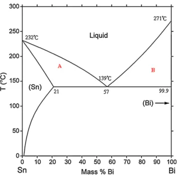
The equilibrium distribution coefficient, the so-called partition coefficient, is the ratio of concentrations of the solid and the liquid in equilibrium, and it is convenient to describe the salient features of these solid–liquid equilibrium relationships. We will take the solidification of the eutectic Bi–Sn composition as an example, as shown at points A and B inFig. 6. Solidification might begin with some phase at a temperature below its melting point and above the eutectic point; thus, we assumed that the starting point is 200◦C, suitable for both cases, and the cooling rate is uniform. If the tem-perature cooled down to 170◦C, the distribution coefficients of Bi and Sn were 0.1 and 0.33 respectively, which indicates once more that under the same solidification conditions Bi phase segregation would consume less of the solute and eject more into the adjacent liquid. That is, the Bi solidification would easily cause enrichment of the adjacent liquid. Because of the alternate enrichments and the difference in distribution coefficient, the variation in segmental lengths was observed.
From the lever rule, the liquid-to-solid ratios of points A and B are 2 and 0.45. While Bi solidified, just one third of the composi-tions were transformed to solid and the rest was ejected into the neighboring liquid. For the same reason, the solidification of tin comparatively utilized an approximate double in solidification.
Fig. 5. STEM image and the element mapping from the framed area of the 220 nm
Bi–Sn eutectic nanowire; (a) the image of a nanowire bundle; (b) the magnified image of framed region; (c) element mapping of Bi; (d) element mapping of Sn.
S.H. Chen et al. / Journal of Alloys and Compounds 481 (2009) 270–273 273
Fig. 6. An example of hypoeutectic (area A), and hypereutectic (area B), composition
points in a binary Bi–Sn phase diagram[38]. 4. Conclusions
A novel segmented appearance was observed in 200 nm eutectic Bi–Sn nanowires which were fabricated by a template-assisted vac-uum hydraulic pressure injection process. That the one-dimension nano-structure of the AAO template limited the banded wire mor-phology to an arrangement along its axis might result from the alternate enrichments between bismuth and tin in the liquid phase. The distribution coefficient and lever rule were utilized to describe the approximately three-fold difference in length. Consequently, when the binary lamellar eutectic was trapped in a nano-scaled structure, the different solidification behavior and the enrichment alternations between hypereutectic and hypoeutectic would bring about this particular appearance.
Acknowledgement
Part of this study was supported by grants from the National Science Council, Taiwan (NSC 97-2218-E-239-005).
References
[1] X.F. Wang, L.D. Zhang, J. Zhang, H.Z. Shi, X.S. Peng, M.J. Zheng, J. Fang, J.L. Chen, B.J. Gao, J. Phys. D 34 (2001) 418–421.
[2] H. Yu, P.C. Gibbons, W.E. Buhro, J. Mater. Chem. 14 (2004) 595–602.
[3] T. Hirata, N. Satake, G.H. Jeong, T. Kato, R. Hatakeyama, K. Motomiya, K. Tohji, Appl. Phys. Lett. 83 (2003) 1119–1121.
[4] Mi. Tian, J. Wang, J. Snyder, J. Kurtz, Y. Liu, P. Schiffer, T.E. Mallouk, M.H.W. Chan, Appl. Phys. Lett. 83 (2003) 1620–1622.
[5] S.H. Jo, J.Y. Lao, Z.F. Ren, R.A. Farrer, T. Baldacchini, J.T. Fourkas, Appl. Phys. Lett. 83 (2003) 4821–4823.
[6] C. Ji, P.C. Season, Appl. Phys. Lett. 81 (2002) 4437–4439.
[7] W.I. Park, D.H. Kim, S.W. Jung, G.C. Yi, Appl. Phys. Lett. 80 (2002) 4232–4234. [8] B.D. Yao, Y.F. Chan, N. Wang, Appl. Phys. Lett. 81 (2002) 757–759.
[9] J.Y. Lao, J.G. Wen, Z.F. Ren, Nano Lett. 2 (2002) 1287–1291.
[10] D. Banerjee, J.Y. Lao, D.Z. Wang, J.Y. Huang, Z.F. Ren, D. Steeves, B. Kimball, M. Sennett, Appl. Phys. Lett. 83 (2003) 2061–2063.
[11] C. Xu, G. Xu, Y. Liu, G. Wang, Solid State Commun. 122 (2002) 175–179. [12] A. Moroz, Phys. Rev. Lett. 83 (1999) 5274–5277.
[13] Z.Q. Liu, Z.W. Pan, L.F. Sun, D.S. Tang, W.Y. Zhou, G. Wang, L.X. Qian, S.S. Xie, J. Phys. Chem. Solids 61 (2000) 1171–1174.
[14] E. Scheil, Z. Metallk 34 (1942) 70–72. [15] W.G. Pfann, Trans. AIME 194 (1952) 747–753.
[16] W. Yang, R.W. Messler, J. Electron. Mater. 23 (1994) 765–772. [17] J. Wanqi, M. Dong, J. Cryst. Growth 156 (1995) 467–472.
[18] C.C. Lee, R.W. Chuang, D.W. Kim, Mater. Sci. Eng. A 374 (2004) 280–284. [19] O.G. Shpyrko, A. Grigoriev, R. Streitel, Phys. Rev. Lett. 95 (2005) 106103. [20] V. Bhattacharya, K. Chattopadhyay, Mater. Sci. Eng. A 449–451 (2007)
1003–1008.
[21] F.Y. Hung, C.J. Wang, S.M. Huang, L.H. Chen, T.S. Lui, J. Alloys Compd. 420 (2006) 193–198.
[22] J. Zhou, Y. Sun, F. Xue, J. Alloys Compd. 397 (2005) 260–264. [23] K. Suganuma, Curr. Opin. Solid State Mater. Sci. 5 (2001) 55–64.
[24] R.A. Islam, B.Y. Wu, M.O. Alam, Y.C. Chen, W. Jillek, J. Alloys Compd. 392 (2005) 149–158.
[25] S.A. Cho, J.L. Ochoa, Metall. Mater. Trans. B 28 (1997) 1081–1087.
[26] C.C. Lee, C.J. Wang, G.S. Matijasevic, IEEE Trans. Components Hybrids Manuf. Technol. 14 (1991) 407–412.
[27] H. Chen, Z. Li, Z. Wu, Z. Zhaung, J. Alloys Compd. 394 (2004) 282–285. [28] C.C. Chen, Y. Bisrat, Z.P. Luo, R.E. Schaak, C.G. Chao, D.C. Lagoudas,
Nanotechnol-ogy 17 (2006) 367–374.
[29] M.C. Flemings:, Solidification Processing, International ed., McGraw-Hill Book Company, Singapore, 1974.
[30] E. Cadirli, H. Kaya, M. Gunduz, J. Alloys Compd. 431 (2007) 171–179. [31] J.M. Song, T.S. Lui, Y.L. Chang, L.H. Chen, J. Alloys Compd. 403 (2005) 191–196. [32] B. Chalmers:, Principles of Solidification, John Wiley & Sons Inc., New York,
1964.
[33] Z.P. Luo, Acta Mater. 54 (2006) 47–58.
[34] M. Straumanis, N. Braaks, Z. Phys. Chem. 29 (1935) 30. [35] M. Straumanis, N. Braaks, Z. Phys. Chem. 37 (1937) 38.
[36] W.D. Winegard, S. Majka, B.M. Thall, B. Chalmers, Can. J. Chem. 29 (1957) 320. [37] G. Tammann, Text Book of Metallography, Chemical Catalogue Co., New York,
1925.
[38] Metallurgy Division, National Institute of Standards and Technology (http://www.metallurgy.nist.gov/phase/solder/bisn.html).