1024 IEEE ELECTRON DEVICE LETTERS, VOL. 33, NO. 7, JULY 2012
A New 4T0.5C AMOLED Pixel Circuit With
Reverse Bias to Alleviate OLED Degradation
Kuei-Yu Lee, Yen-Ping Hsu, and Paul C.-P. Chao, Member, IEEE
Abstract—A new 4T0.5C circuit is proposed to achieve a
high-resolution active-matrix organic light-emitting diode (OLED) dis-play with the capability of alleviating OLED degradation, while the panel nonuniformity is compensated by an already-proposed system. The designed circuit is built on two adjacent pixels with eight transistors and one capacitor, thus equivalently as a 4T0.5C pixel circuit in occupied layout area. In this circuit, a single storage capacitor is shared by the two adjacent pixels to minimize the entire layout area. The minimized pixel size is compatible to a con-ventional 2T1C pixel circuit. Along with this 4T0.5C circuit, a new alternative drive scheme is developed to address the panel. The scheme offers the function of automatic reverse biasing on OLEDs to alleviate degradation. The designed circuit is fabricated, and the performance of OLED degradation is successfully validated.
Index Terms—Active-matrix organic light-emitting diode (AMOLED), degradation, reverse bias.
I. INTRODUCTION
A
CTIVE-MATRIX organic light-emitting diode (OLED) (AMOLED) displays have drawn much attention due to various advantages, such as high brightness, high efficiency, and wide viewing angle. However, they face the serious prob-lems like emission nonuniformity of panel and OLED life-time degradation. Panel nonuniformity is improved with the advances in TFT fabrication processing and developed com-pensation methods [1]–[3]. In [1] and [2], a self-comcom-pensation pixel circuit was designed, but it occupied the layout area of six transistors and one capacitor. Other researchers in [3] proposed the external compensation system to remedy draw-backs of panel nonuniformity without extra TFTs in a pixel circuit, which is the future design trend for high-resolution AMOLED displays. On the other hand, the lifetime degradation in OLED emitted luminance is always another serious problem, which is detrimental as the AMOLED display is expected to replace large-sized and full high-definition LCD televisions. The degradation on OLED lifetime is generally induced by high-density currents under long-time driving [4]. Some com-pensation methods were developed in few past works to solve the problem. Estimating OLED degradation by detecting its cross-voltage in a long-time driving, the study in [5] proposed a current compensation approach, where the current through an OLED component was intentionally adjusted larger to maintainManuscript received February 16, 2012; revised April 6, 2012; accepted April 8, 2012. Date of publication May 21, 2012; date of current version June 22, 2012. This work was supported in part by the Taiwan National Science Council I-RiCE Program under Grant NSC-100-2911-I-009-101. The review of this letter was arranged by O. Manasreh.
The authors are with the National Chiao Tung University, Hsinchu 300, Taiwan (e-mail: [email protected]; [email protected]; pchao@mail. nctu.edu.tw).
Color versions of one or more of the figures in this letter are available online at http://ieeexplore.ieee.org.
Digital Object Identifier 10.1109/LED.2012.2194983
originally designed emitted luminance. However, it often ag-gravates OLED degradation due to larger currents. Some other studies imposed reverse biases on an OLED component in the nonemission period for alleviating OLED lifetime degradation [6], [7]. However, as realizing the designs in [1], [2], and [5], for current compensation and degradation alleviation, more circuit components are required. In this way, the pixel size is increased, then decreasing significantly the resolution of the OLED display.
To maintain OLED display resolution, a new 4T0.5C pixel circuit capable of OLED degradation alleviation is designed in this study. The designed pixel circuit is assumed equipped with an already-proposed external compensation system like in [3] to tackle potential problems of TFT nonuniformity and voltage drop. This designed 4T0.5C pixel consists of four transistors and a storage capacitor shared by two adjacent pixels. The proposed driving algorithm enables the operations of reverse bias to alleviate OLED degradation. Based on a common design rule that the area of a storage capacitor is equivalent to that of three transistors, the area occupied by the 4T0.5C pixel is equivalent to that of 2.5T1C. Since the pixel area of 2.5T1C is close to that of the baseline 2T1C circuit, the desired resolution of the AMOLED display is able to be maintained as the same level of high-resolution display with the function of alleviating OLED degradation. Moreover, the proposed circuit is easy to be combined with an external system to compensate panel nonuni-formity due to TFT threshold drift and voltage drop across the panel, since the operation principle of the pixel circuit is identical with that of the 2T1C pixel circuit. The designed 4T0.5C pixel circuit is fabricated in this study and tested to demonstrate satisfactory performance for OLED degradation alleviation.
II. OPERATION OF THE4T0.5C PIXELCIRCUIT
Fig. 1 shows the designed circuit topology for the proposed 4T0.5C pixel circuit, where the circuits for two 4T0.5C pixels are included. One is denoted as “upper,” while the other is denoted as “lower,” as shaded in different colors in the figures. In Fig. 1, T1, T3, T5, T7, and OLED1constitute the upper pixel, while T2, T4, T6, T8, and OLED2 constitute the lower pixel.
OLED1and OLED2represent the two OLED components in new 4T0.5C pixel circuits. Switches T1and T2are controlled by the scan line signals in a conventional display technique Vscan1 and Vscan2. T3 and T4 are the switches controlling discharge paths. T5 and T6 are two distinct TFTs to drive alternatively
OLED1 and OLED2 for light emission. T7 and T8 are de-signed to realize operation of reverse bias to alleviate OLED degradation. The storage capacitor C is shared by two 4T0.5C pixels in order to save layout area for higher resolution displays.
LEE et al.: NEW 4T0.5C AMOLED PIXEL CIRCUIT WITH REVERSE BIAS TO ALLEVIATE OLED DEGRADATION 1025
Fig. 1. 4T0.5C pixel circuit.
Fig. 2. (a) Timing diagrams of control signals. (b) Voltage levels in the pixel circuit.
Fig. 3. Driving currents.
Fig. 2(a) shows the timing diagrams of control signals. Each frame time for the designed 4T0.5C pixel circuit is divided into two periods that are named upper and lower pixel emissions. To realize alternative-drive and reverse biasing, specific signals
Vs1 and Vs2 are designed to control T4 and T8, and T3 and
T7, respectively. Vg1and Vg2 are the gate voltages for driving
TFTs T5and T6. VOLED1and VOLED2are the anode voltages applied to the OLED components, as shown in Fig. 2(b). Fig. 3 shows the timing diagrams of driving currents to OLED1and
OLED2 in the two 4T0.5C pixels, denoted by IOLED1 and
IOLED2, respectively. The basic drive principle is that the upper pixel emits light when the lower pixel is experiencing current off and operated in reverse bias, as shown in Figs. 2 and 3. On the contrary, the lower pixel emits when the upper pixel is in current-off period and operates in reverse bias period.
During the charge period of upper pixel emission, as shown in Fig. 2(a), Vscan1 is set to a low voltage level, while T1 is turned on. Meanwhile, Vs1is at low voltage, while T4is turned on. Vs2 is set to a high voltage level such that T3 and T7 are turned off. At this moment, the shared storage capacitor C is charged until Vg1reaches Vdatain order to set the emitted gray level by the upper pixel. Meanwhile, Vg2reaches Vdd, causing
Fig. 4. Monte Carlo simulation of average current variations on (a) the conventional 2T1C pixel circuits without compensating [2] and (b) the proposed 4T0.5C pixel circuits using an external compensation system.
the driving TFT T6in the lower pixel to be turned off. T8is then operated to produce a reverse bias between VOLED2and Vssfor alleviating degradation of OLED2. During the period of upper pixel emission, OLED2 is in the status of nonemission and reverse bias. During the charge period of lower pixel emission,
Vscan2is at a low voltage level within the first half of a frame time, while T2 is turned on. Vs2 is also set to a low voltage,
while T3 is turned on and T7 is operated to produce reverse bias between VOLED1and Vss, as shown in Fig. 2(b). Following the operation, OLED1 and OLED2 alternatively either emit programmed luminance or experience reverse bias at any given moment. For the proposed 4T0.5C pixel circuit, the frame time frequency of the panel is also set as 60 Hz, like a conventional pixel circuit. However, the 4T0.5C pixel circuit operates with an interlaced scan (odd rows first and then even rows) rather than the conventional progressive scan. The gray levels of OLED1 and OLED2 are refreshed alternatively in two halves of the frame time, as shown in Fig. 2(a). In the results, the interlaced scan leads to a nonemission period for each pixel within a frame time. The nonemission period is designed for applying reverse bias to alleviate OLED degradation.
In this way, the 4T0.5C circuit has the capability of combin-ing OLED degradation alleviation with an external compensa-tion system to compensate panel nonuniformity. The validated compensation results are based on the Monte Carlo simulations of average driving currents through OLED components. The parameter variations are set following realistic data as given in [2]. The “Vdata’s” of the proposed 4T0.5C pixel circuits using an external compensation method like in [3] are designed to store compensation information, while they are input into pixel circuits for investigating the variations of average driving cur-rents. Fig. 4(a) and (b) shows resulted simulated average OLED currents for both the conventional 2T1C and the proposed 4T0.5C for comparison. The current variation of the proposed circuit is
±1.08%, which is superior to ±19.27% resulted from 2T1C.
III. FABRICATION ANDEXPERIMENTRESULTS
To validate the performance of saving layout area, a trial fabrication process is designed and carried out to show a low level of pixels per inch (ppi). The well-known process of low-temperature polysilicon TFT using the excimer laser annealing is employed. Aspect ratios (W/L) of switching TFTs T1, T2,
T3, T4, T7, and T8are all designed to be 4 μm/4 μm. Aspect ratios of driving TFTs T5 and T6 are both designed to be 4 μm/20 μm. The shared capacitor C is designed to have 0.1 pF. Fig. 5(a) shows a microphotograph of the fabricated pixel, where two squares are assumed for two VIA contact areas to OLEDs in a typical top-emission AMOLED panel. As results,
1026 IEEE ELECTRON DEVICE LETTERS, VOL. 33, NO. 7, JULY 2012
Fig. 5. (a) Microphotograph of the fabricated pixel. (b) Experiment setup to investigate OLED degradation alleviation.
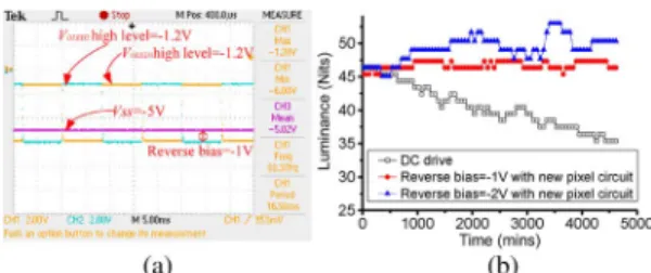
Fig. 6. (a) VOLED1, VOLED2, and Vsssignals while operating with a reverse
bias of−1 V. (b) Measurement on OLED luminance for testing degradation alleviation.
each 4T0.5C pixel circuit occupies 131.25× 43.75 μm2, which is about 200 ppi, commonly regarded as a high resolution [8].
A drive circuit panel containing 100 pixels is fabricated and then wire bonded to a single large OLED die of 0.3× 0.3 cm2. A large size of 0.3× 0.3 cm2 is intended for larger OLED drive currents and easy measurement on emitted light power. Fig. 5(b) shows the experimental setup, in which the OLED die is attached at the bottom to an aluminum board. The temper-ature of the board is controlled at room tempertemper-ature, 23.8◦C, using a commercialized control unit and based on the feedback signals from a thermostat. The achieved constant-temperature environment rules out the temperature effects on OLED emitted luminance. This enables the investigation on the degradation based on measured OLED luminance. For the experiment, Vdd is set to a dc of 8 V and Vss is set to a dc of−5 V as designed previously, while Vdatais set to a dc of 1 V from power supply. As for Vscan’s and Vs’s, they are generated by an FPGA board
and then powered by operational amplifiers that are responsible for level shifting. Scan line signals Vscan1 and Vscan2 are set from−5 to 10 V, while enabling signals of reverse bias Vs1and Vs2are set from −10 to 10 V. Waveforms of Vscan’s and Vs’s
were previously designed, as shown in Fig. 2(a). Fig. 6(a) shows the signals measured from the fabricated pixel circuit, where basic characteristics of these 4T0.5C pixel circuits are presented as expected, including a reverse bias operation. A colorimeter BM-7 is utilized to measure the luminance for extensive time periods. This is intended to validate the effects of degradation alleviation. The measurement for a blue OLED driven by two different levels of reverse bias and a dc is shown in Fig. 6(b). The blue OLED is chosen for discussion since it degrades most
as compared to other OLEDs of different colors. It is seen from Fig. 6(b) that the OLED under dc drive shows serious luminance degradation. The OLEDs under reverse biases in levels of −1 and −2 V provide sustainable and even slightly increased emitted luminance. These luminance increases result from the fact that the electrons are trapped into gate insulators of TFTs for a long time of operation [9]. However, they are confined to ±5% of the originals, which are about in the same level as common TFT nonuniformities due to threshold shifts. Therefore, the performance of degradation alleviation offered by the designed new 4T0.5C pixel circuit is successfully validated.
IV. SUMMARY
A new 4T0.5C pixel circuit with an external compensation system has been designed to implement the function of reverse bias for OLED degradation alleviation. In the pixel layout, each capacitor is shared by two pixels, resulting in a significant reduction in pixel layout area. The resulted pixel resolution reaches as much as 200 ppi. A realistic pixel circuit panel along with OLEDs to drive is fabricated to realize the proposed function of reverse bias on the OLEDs in order to test the performance of degradation alleviation. It is found that the proposed circuit and its driven algorithm are able to sustain emitted luminance level for an extensive period of time, while the OLED driven by a bias dc suffers severe degradation in emitted luminance.
ACKNOWLEDGMENT
The authors would like to thank AU Optronics Corporation, Hsinchu, Taiwan, for their assistance to fabricate the organic light-emitting diode pixel circuit.
REFERENCES
[1] J. H. Lee, J. H. Kim, and M. K. Han, “A new a-Si:H TFT pixel circuit compensating the threshold voltage shift of a-Si:H TFT and OLED for active matrix OLED,” IEEE Electron Device Lett., vol. 26, no. 12, pp. 897– 899, Dec. 2005.
[2] K. Y. Lee and C. P. Chao, “A new AMOLED pixel circuit with pulsed drive and reverse bias to alleviate OLED degradation,” IEEE Trans. Electron
Devices, vol. 59, no. 4, pp. 1123–1130, Apr. 2012.
[3] H. J. In and O. K. Kwon, “External compensation of nonuniform electrical characteristics of thin-film transistors and degradation of OLED devices in AMOLED displays,” IEEE Electron Device Lett., vol. 30, no. 4, pp. 377– 379, Apr. 2009.
[4] J. Shen, D. Wang, E. Langlois, W. A. Borrow, P. J. Green, C. W. Tang, and J. Shi, “Degradation mechanisms in organic light emitting diodes,”
Syn-thetic Metals, vol. 111-112, pp. 233–236, Jun. 2000.
[5] C. L. Lin and Y. C. Chen, “A novel LTPS-TFT pixel circuit compensating for TFT threshold-voltage shift, and OLED degradation for AMOLED,”
IEEE Electron Device Lett., vol. 28, no. 2, pp. 129–131, Feb. 2007.
[6] M. Yahiro, D. Zou, and T. Tsutsui, “Recoverable degradation phenomena of quantum efficiency in organic EL devices,” Synthetic Metals, vol. 111/112, pp. 245–247, Jun. 2000.
[7] Y. J. Si, L. Q. Lang, Y. Zhao, X. F. Chen, and S. Y. Liu, “Improvement of pixel electrode circuit for active-matrix OLED by application of reversed-biased voltage,” IEEE Trans. Circuits Syst. II, Exp. Briefs, vol. 52, no. 12, pp. 856–859, Dec. 2005.
[8] T. Kohno, H. Kageyama, M. Miyamoto, M. Ishii, N. Kasai, N. Nakamura, and H. Akimoto, “High-speed programming architecture and image-sticking cancellation technology for high-resolution low-voltage AMOLEDs,” IEEE Trans. Electron Devices, vol. 58, no. 10, pp. 3444– 3452, Oct. 2011.
[9] M. Matsumura, M. Hatano, T. Shiba, and M. Ohkura, “Degradation char-acteristics of n- and p-channel polycrystalline-silicon TFTs under CMOS inverter operation,” IEEE Trans. Electron Devices, vol. 57, no. 2, pp. 429– 436, Feb. 2010.