IEEE ELECTRON DEVICE LETTERS, VOL. 34, NO. 12, DECEMBER 2013 1551
Novel Cu-to-Cu Bonding With Ti Passivation
at 180 °C in 3-D Integration
Yan-Pin Huang, Yu-San Chien, Ruoh-Ning Tzeng, Ming-Shaw Shy, Teu-Hua Lin, Kou-Hua Chen,
Chi-Tsung Chiu, Jin-Chern Chiou, Member, IEEE, Ching-Te Chuang, Fellow, IEEE,
Wei Hwang, Fellow, IEEE, Ho-Ming Tong, Fellow, IEEE,
and Kuan-Neng Chen, Senior Member, IEEE
Abstract— A novel CMOS-compatible bond structure using Cu-to-Cu bonding with Ti passivation is demonstrated at low temperature and investigated. With the Ti protection of inner Cu, Cu bonding temperature can be reduced to 180 °C. In addition, excellent electrical stability against humidity and temperature cycling is achieved. Diffusion behavior and mechanism of Cu and Ti are also discussed. With excellent bond results and reliability, this bonded scheme has the potential to be applied in 3-D integration.
Index Terms— 3-D integration, Cu bonding, Ti passivation. I. INTRODUCTION
L
ITHOGRAPHY and physical limitation will bring up the bottleneck of developing new semiconductor fabrication in the near future. 3-D integration is one of the most promising candidates for the solution, as well as the realization of heterogeneous integration. 3-D integration has advantages of high function density, small form factor, and high performance [1]–[3]. In 3-D integration bonding technology, one of the key technologies currently uses metals for the stacking medium as the mainstream, especially copper with its outstanding electrical properties. Conventional Cu-Cu bonding can provide excellent resistance toward electromigration, thermal stressing, and mechanical stress. However, the required bonding temper-ature is>300 °C to achieve good results [4]. The high bonding temperature may result in the misalignment, residual thermal stress, high cost, and low throughput [5].In this letter, a novel bond structure using Ti as the pas-sivation layer on Cu surface is proposed and developed at low temperature of 180 °C. With the interdiffusion behavior of copper and titanium during thermal compression process, Cu-to-Cu bonding can be completed and a continuous Cu layer is formed between two Ti layers. With the excellent bond results, it is recommended that Cu-to-Cu bonding with Manuscript received September 25, 2013; accepted October 9, 2013. Date of publication October 30, 2013; date of current version November 20, 2013. This work was supported in part by the Ministry of Education in Taiwan under the ATU Program, in part by the Advanced Semiconductor Engineering Group, and in part by the National Science Council through Grant NSC 101-2628-E-009-005 and Grant NSC 102-2221-E-009-160. The review of this letter was arranged by Editor K. Uchida.
Y.-P. Huang, Y.-S. Chien, R.-N. Tzeng, J.-C. Chiou, C.-T. Chuang, W. Hwang, and K.-N. Chen are with the National Chiao Tung University, Hsinchu 300, Taiwan (e-mail: [email protected]).
M.-S. Shy, T.-H. Lin, K.-H. Chen, C.-T. Chiu, and H.-M. Tong are with the Advanced Semiconductor Engineering Group, 32016 Kaohsiung, Taiwan.
Color versions of one or more of the figures in this letter are available online at http://ieeexplore.ieee.org.
Digital Object Identifier 10.1109/LED.2013.2285702
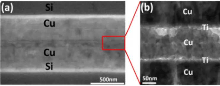
Fig. 1. Cu/Cu with Ti passivation bonded results. (a) SEM. (b) TEM.
Ti passivation can be a promising method for low-temperature bonding technology.
II. EVALUATION OFCu/Ti–Ti/Cu BONDEDSTRUCTURE 300-nm Cu layer followed by 5–10-nm Ti passivation layer on Cu surface was deposited on Si substrate sequentially, under a working pressure of 7× 10⁻³ torr and with a base pressure of 1× 10⁻⁶ torr. There is no surface treatment needed before thermal compression bonding process due to the application of Ti passivation on copper. These samples were bonded face-to-face at 1.91 MPa and 180 °C for 30–50 min. The morphology and element analysis of the bonded structure were analyzed by SEM, TEM, EDX, and AES.
The cross-sectional view of the bonded structure in Fig. 1(a) shows a well-bonded result without voids and cracks. Sur-prisingly, the bonded interface morphology shows the two Ti layers on Cu surface are not at original bonded interface anymore, but a Cu layer between them instead, as shown in Fig. 1(b). Fig. 2(a) and (b) shows TEM image and EDX analysis. As shown in Fig. 2(b), Ti/TiOx moved toward Si substrate, while Cu moved to original bonding interface, further performed Cu-to-Cu bonding at low temperature. This result suggests an interdiffusion behavior was involved during bonding.
To evaluate the interdiffusion behavior, one Cu sam-ple with Ti layer at the surface before and after 400 °C 60-min N2anneal was examined by Auger analysis, as shown in Fig. 3(a) and (b). Since Ti is easily oxidized, a very thin Ti oxide layer (<5 nm) is observed on the surface in Fig. 3(a). No oxygen in the entire copper region indicates that Ti has successfully protected inner Cu from oxidation. After 400 °C 60-min N2 anneal, Fig. 3(b) shows some Cu has diffused out of Ti layer and become surface layer. 0741-3106 © 2013 IEEE
1552 IEEE ELECTRON DEVICE LETTERS, VOL. 34, NO. 12, DECEMBER 2013
Fig. 2. (a) TEM image of the Cu/Cu bonding with Ti passivation and the EDX scanning position. (b) Corresponding EDX composition profile.
Fig. 3. Auger depth profiles of Cu layer with Ti passivation. (a) Before annealing. (b) After annealing at 400 °C for 60 min.
Due to lower activation energy at the surface, Cu has a tendency to diffuse toward surface. In contrast, Ti/TiOX tends to diffuse toward Si substrate [6]–[8]. This phenomenon has been observed in metal films in previous studies as well [8], [9]. Therefore, during bonding process, Cu diffused to surface from two samples can be bonded together without Cu oxides involved.
III. SCHEMATIC OFBONDINGPROCEDURE
Based on previous discussion, Cu/Ti–Ti/Cu bond structure could be a potential option for interconnects in 3-D integration. Fig. 4 shows the schematic diagram of the Cu/Ti–Ti/Cu bonding procedure. At first, Ti on the surface protects inner Cu before bonding. During bonding process, some Cu atoms diffuse toward the bonding interface and form a new surface layer, while Ti/TiOXatoms move toward the substrate. Finally, Cu atoms of new surface layers from the top and bottom samples perform bonding and merge into a continuous layer. Since Ti is a CMOS compatible material, this bond structure can be employed in current semiconductor process with cost benefit.
Fig. 4. Schematic diagram of Cu-to-Cu bonding with Ti passivation.
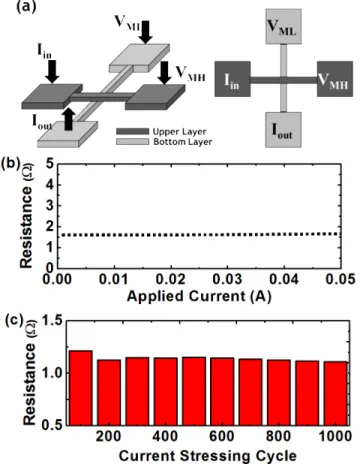
Fig. 5. Contact resistance measurement of the bonded structure. (a) Schematic diagram and top view. (b) Before current cycling. (c) After 1000 current cycling.
IV. ELECTRICALMEASUREMENT AND RELIABILITYINVESTIGATION
Contact resistance of the bonded structure was evaluated by a modified Kelvin structure, which has been used in
HUANG et al.: NOVEL Cu-TO-Cu BONDING WITH Ti PASSIVATION 1553
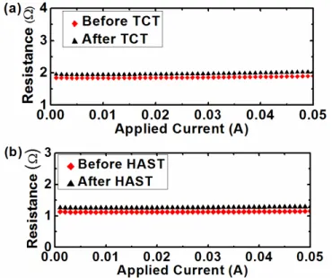
Fig. 6. Contact resistance measurement of the bonded structure. (a) Before and after temperature cycling test. (b) Before and after unbias HAST. 3-D integration [10]–[11]. Fig. 5(a) shows the schematic diagram and top view of this test structure. Fig. 5(b) shows resistance measurement results of one Cu/Ti–Ti/Cu bonded structure under different applied current, demonstrating a good structural and electrical stability after bonding. The measured resistance of bonded structure is compatible to that of current products, demonstrating the feasibility of manufacturing.
In addition, this bonded scheme was investigated again after multiple current stressing, where each stressing was swept from −100 to 100 mA. As shown in Fig. 5(c), even after 1000 multiple current stressing cycles, the resistance of bond structure does not change much and keeps stable, indicating a reliable performance after electrical operation.
Since the reliability is an important concern in 3-D inte-gration, the bonded structure was also evaluated with thermal cycling test (TCT) and unbias highly accelerated stress test (unbias HAST). The resistance measurement result of one bonded structure after TCT treatment is shown in Fig. 6(a). TCT was performed with temperature cycling from −55 °C to 125 °C (JESD22-A104B) to assess thermal reliability. As shown in Fig. 6(a), after 500 thermal cycling loop treat-ments, the resistance of the bonded structure is still stable and even has a slight decrease, which may come from the quality improvement of bonding interface during TCT [12].
The unbias HAST (JESD22A-118) was performed at 85% RH and 130 °C for 96 h. Fig. 6(b) shows the resistance
measurement result of another bonded structure after the unbias HAST. It can be seen that the resistance also stays stable after unbias HAST. The resistance after unbias HAST has also a slight decrease, which is similar to that after TCT treatment. These results suggest that this Cu bond structure with Ti passivation can be effective ability against the corro-sion and degradation caused by environment.
V. CONCLUSION
A novel Cu bond structure utilizing Ti passivation layer has been proposed for low-temperature bonding technology in 3-D integration. Both electrical performances and reliability results demonstrate that this bonded scheme is stable and has high resistance against temperature and humidity degradation, and suitable for low temperature 3-D integration applications.
REFERENCES
[1] D. Sylvester and C. Hu, “Analytical modeling and characterization of deep-submicrometer interconnect,” Proc. IEEE, vol. 89, no. 5, pp. 634–664, May 2001.
[2] A. Rahman and R. Reif, “System-level performance evaluation of three-dimensional integrated circuits,” IEEE Trans. Very Large Scale Integr.
(VLSI) Syst., vol. 8, no. 6, pp. 671–678, Dec. 2000.
[3] V. W. C. Chan, P. C. H. Chan, and M. Chan, “Multiple layers of CMOS integrated circuits using recrystallized silicon film,” IEEE Electron
Device Lett., vol. 22, no. 2, pp. 77–79, Feb. 2001.
[4] K. N. Chen, A. Fan, C. S. Tan, et al., “Bonding parameters of blanket copper wafer bonding,” J. Electron. Mater., vol. 35, no. 2, pp. 230–234, 2006.
[5] K. T. Ko and K. N. Chen, “Low temperature bonding technology for 3D integration,” Microelectron. Rel., vol. 52, pp. 302–311, Feb. 2012. [6] P. A. Korzhavyi, I. A. Abrikosov, B. Johansson, et al., “First-principles
calculations of the vacancy formation energy in transition and noble metals,” Phys. Rev. B, vol. 59, no. 18, pp. 11693–11703, May 1999. [7] E. S. Machlin, An Introduction to Aspects of Thermodynamics and
Kinetics Relevant to Materials Science. Burlington, MA, USA: Elsevier,
2007, pp. 248–252.
[8] S. Tsukimoto, T. Kabe, K. Ito, et al., “Effect of annealing ambient on the self-formation mechanism of diffusion barrier layers used in Cu(Ti) interconnects,” J. Electron. Mater., vol. 36, no. 3, pp. 258–265, 2007.
[9] S. Y. Hsu, H. Y. Chen, and K. N. Chen, “Cosputtered Cu/Ti bonded interconnects with a self-formed adhesion layer for three-dimensional integration applications,” IEEE Electron Device Lett., vol. 33, no. 7, pp. 1048–1050, Jul. 2012.
[10] K. N. Chen, A. Fan, and C. S. Tan, “Contact resistance measure-ment of bonded copper interconnects for three-dimensional integration technology,” IEEE Electron Device Lett., vol. 25, no. 1, pp. 10–12, Jan. 2004.
[11] P. Gueguen, L. Di Cioccio, P. Morfouli, et al., “Copper direct bonding: An innovative 3D interconnect,” in Proc. IEEE Electron. Compon.
Technol. Conf., Jun. 2010, pp. 878–883.
[12] Y. J. Chang, C. T. Ko, and K. N. Chen, “Electrical and reliability investigation of Cu TSVs with low-temperature Cu/Sn and BCB hybrid bond scheme,” IEEE Electron Device Lett., vol. 34, no. 1, pp. 102–104, Jan. 2013.