Hole Schottky barrier height enhancement and its application to
metal–semiconductor–metal photodetectors
S. D. Lin and C. P. Lee
Citation: Journal of Applied Physics 90, 5666 (2001); doi: 10.1063/1.1415060
View online: http://dx.doi.org/10.1063/1.1415060
View Table of Contents: http://scitation.aip.org/content/aip/journal/jap/90/11?ver=pdfcov Published by the AIP Publishing
Articles you may be interested in
Low-temperature grown GaAs heterojunction metal-semiconductor-metal photodetectors improve speed and efficiency
Appl. Phys. Lett. 99, 203502 (2011); 10.1063/1.3662392
Metal-semiconductor-metal photodetectors based on single-walled carbon nanotube film–GaAs Schottky contacts
J. Appl. Phys. 103, 114315 (2008); 10.1063/1.2938037
Mixing characteristics of InGaAs metal–semiconductor–metal photodetectors with Schottky enhancement layers Appl. Phys. Lett. 82, 3814 (2003); 10.1063/1.1579117
Ultrahigh power-bandwidth-product performance of low-temperature-grown-GaAs based metal-semiconductor-metal traveling-wave photodetectors
Appl. Phys. Lett. 80, 4054 (2002); 10.1063/1.1482139
InGaAs metal-semiconductor-metal photodetectors with a hybrid combination of transparent and opaque electrodes
Appl. Phys. Lett. 70, 3026 (1997); 10.1063/1.118738
Hole Schottky barrier height enhancement and its application to
metal–semiconductor–metal photodetectors
S. D. Lin and C. P. Leea)
Department of Electronics Engineering, National Chiao Tung University, 1001 Ta Hsueh Road, Hsinchu, Taiwan, Republic of China
共Received 25 April 2001; accepted for publication 4 September 2001兲
Hole Schottky barrier heights on GaAs have been studied experimentally by using a conventional metal–semiconductor–metal photodetector 共MSMPD兲 structure. The Schottky barrier height for holes was obtained directly by the hole-current dominated dark current measurement of the MSMPD. With a thin, highly doped surface layer, control of the Schottky barrier heights for holes from 0.48 to 0.79 eV was obtained. By using these engineered Schottky contacts in the MSMPDs, over three orders of magnitude reduction in the dark currents of the MSMPDs was achieved. © 2001 American Institute of Physics. 关DOI: 10.1063/1.1415060兴
I. INTRODUCTION
It is well known that the Schottky barrier height in many semiconductors is relatively insensitive to the metal used be-cause of the pinning of the Fermi surface level. This is par-ticularly true for GaAs.1–3The Schottky barrier height is an important parameter for many devices, such as field-effect transistors 共FET兲, high-mobility electron transistors 共HEMT兲, and metal–semiconductor–metal photodetectors 共MSMPDs兲. Adjusting the barrier height to a desirable value can lead to the improvement of device performance. Among various methods to control the Schottky barrier heights,4 –11 using a thin, highly doped interfacial layer is most effective and has been used for a long time. In 1974, Shannon showed that the Schottky barrier heights for electrons and for holes on silicon could be controlled by ion-implanted layers.8 Fol-lowing that work, the method was applied to other semicon-ductors, e.g., GaAs,2,9 InP,10 and InGaAs.11 A thin surface epilayer has also been used to modify the Schottky barrier heights. However, most of these investigations have been focused on the Schottky barrier height for electrons (bn)
only, and the studies of Schottky barrier height for holes (b p) are relatively few. Among the reported results on hole
Schottky barrier heights, the modification was achieved by introducing an additional layer 共e.g., metal, semiconductor, or insulator兲.4 –7The modified hole Schottky barrier heights were measured by using p-type GaAs on a p⫹-GaAs sub-strate. Results showed that the barrier heights can be con-trolled in the range of 0.4 –0.9 eV and the sums of the elec-tron and hole Schottky barrier heights are equal to or less than the GaAs band-gap energy.
In a conventional, unmodified Schottky diode, the sum of the electron and the hole Schottky barrier heights is equal to the energy gap of the semiconductor.3That is,
bn⫹b p⫽Eg. 共1兲
This relation has been proven by experiments on many kinds of semiconductors.1,12From Eq.共1兲 one can easily determine
the hole Schottky barrier height once the electron Schottky barrier height is known. This is why there is no need to study the hole Schottky barrier height directly. However, for the modified Schottky diode with a thin, highly doped layer, the equality may not be correct anymore. In the following, the reason is explained by an example of an n-type Schottky diode with a thin p⫹ layer between the metal and the semi-conductor. Assuming that the doping concentrations of the
n-type semiconductor and the thin p⫹layer are NDand NA, respectively, and d is the thickness of the p⫹layer, according to the depletion model, the enhancement of the electron Schottky barrier height (⌬bn) is
⌬bn⫽ qNA
2s
d2, 共2兲
where q is the unit electron charge, and s is the dielectric
constant of the semiconductor.3,8 On the other hand, the re-duction of the hole Schottky barrier height consists of two major contributions. The first, indicated by⌬b p1, is caused
by image force lowering due to an enhanced electric field at the interface. It can be estimated by the formula below3
⌬b p1⫽ q
s
冑
NAd4. 共3兲
The other one is the enhancement of the tunneling current of holes. By the calculation of Shannon in 1974,8the amount of reduction will be significant if the electric field at the inter-face is larger than about 105 V/cm, i.e., N
Ad⬎1012 cm⫺2.
The quantity of the reduction of the hole Schottky barrier height contributed from the tunneling current depends on the hole’s effective mass and the surface electric field, etc., so the equality in Eq. 共1兲 obviously fails. In general, the sum-mation of the electron and the hole Schottky barrier heights is larger than the energy gap of the semiconductor. That is why the direct measurement of hole Schottky barrier height is necessary in these modified Schottky diodes.
In the present article, we investigated the hole Schottky barrier height on GaAs by using a conventional metal– semiconductor–metal 共MSM兲 photodetector structure. The a兲Electronic mail: [email protected]
5666
0021-8979/2001/90(11)/5666/4/$18.00 © 2001 American Institute of Physics
structure consists of two back-to-back Schottky diodes. Ig-noring the two-dimensional and the image force lowering effects, under the flatband condition, i.e., the semiconductor between two metal contacts totally depleted, the total current
Jtthrough the structure can be describe approximately by the
simple relation:
Jt⫽Jn⫹Jp⫽An*T
2e⫺qbn/kT⫹A p
*T2e⫺qb p/kT, 共4兲 where Jn(Jp) is the electron共hole兲 current injecting from the
cathode共anode兲, and An*(Ap*) is the Richardson’s constant of the electron共hole兲.13For GaAs, the Richardson’s constant of electrons is about an order smaller than that of the holes.3 Therefore the hole current Jp will be dominant if b p is
equal or less thanbn. In this case the hole Schottky barrier
height b p can be obtained from the dark current measure-ment of the MSM photodetector. In addition, we also studied the modified Schottky contacts containing a thin, highly doped GaAs layer by the same structure. For a 15 nm, 2 ⫻1018cm⫺3Si-doped layer, a reduction of over three orders
of magnitude for the dark current for the MSM photodetector was achieved.
II. EXPERIMENT
A. Sample growth and device fabrication
The samples used for this study were grown by molecu-lar beam epitaxy using a Varian GEN II system. The sample structure is schematically shown in Fig. 1. The structure con-sists of, starting from the 共100兲 semi-insulating GaAs sub-strate and the GaAs buffer layer, a 200 nm Al0.35Ga0.65As
layer, a 1m GaAs layer, and a 15 nm GaAs layer. All layers except the top 15 nm of GaAs were undoped. Five samples (N1, N2, N3, P, and U兲 with the same structure were grown to study the doping effect of the top layer. Samples N1, N2, and N3 were Si-doped with concentrations of 5⫻1017, 1⫻1018,
and 2⫻1018 cm⫺3, respectively. Sample P was Be-doped with a concentration of 1⫻1018 cm⫺3, and for comparison sample U had an undoped top layer. In order to minimize the effect of the dopant diffusion during growth, the substrate temperature was decreased from the normal growth tempera-ture of 575 °C to about 540 °C before the top layer growth. In fact, the structure of sample U is exactly the same as a con-ventional MSMPD.14 In the structure, the undoped GaAs layer is the absorption layer, and the AlGaAs layer is the absorption stop layer, to prevent the photogenerated carriers in the substrate from being collected by the electrodes of the
photodetector. Besides, because the characteristics of Schottky contacts are very sensitive to the process proce-dures, a sample with the structure of a conventional Schottky diode was grown on 共100兲 n⫹-GaAs substrate. This sample served to monitor the process conditions of other samples.
All five samples were processed together. The process was basically the same as that of the conventional MSMPDs, i.e., it was composed of three main steps: finger metalliza-tion, dielectric passivation and isolametalliza-tion, and pad formation. Three different devices were fabricated on each sample. They consist of conventional MSMPDs with both electrodes on the top layer, MSMPDs with one electrode on the top layer and the other on the absorption layer, i.e., the surface on which the top layer was etched off, and MSMPDs with both electrodes on the absorption layer. In this study they are called T 共top兲, A 共asymmetry兲, and B 共bottom兲 devices, re-spectively. A schematic of the three devices is shown in Fig. 2. The Schottky metal used was Ti/Pt/Au, with a thickness of 30 nm/30 nm/100 nm. Before the top metal deposition, the samples were treated with an UV/ozone stripper, and then dipped in HCl/H2O共1:1兲 for 30 s to remove surface
contami-nants and native oxide. After both finger electrodes were formed, a surface passivation layer of 150 nm silicon-oxide (SiOx) was deposited using plasma-enhanced chemical
va-por deposition 共PECVD兲. In the finished devices, the finger spacing was 6 m and the active area was 200⫻200m2.
During the device processing, the conventional Schottky diodes were fabricated at the same time. Two diodes were prepared, one with the Schottky metal on the as-grown sur-face 共denoted as ST兲, and the other with the schottky metal on an etched surface 共denoted as SB兲.
B. Result and discussion
The current–voltage characteristics of all devices were measured with a HP4145 semiconductor parameter analyzer
FIG. 1. A schematic diagram of the layer structures of samples N1 共ND
⫽5⫻1017 cm⫺3兲, N
2 共ND⫽1⫻1018 cm⫺3兲, N3 共ND⫽2⫻1018 cm⫺3兲, P共NA⫽1⫻1018cm⫺3兲, and U 共undoped兲 used in the study.
FIG. 2. A schematic diagram of the three kinds of devices: T, B, and A. 5667
J. Appl. Phys., Vol. 90, No. 11, 1 December 2001 S. D. Lin and C. P. Lee
on a probe station. The conventional Schottky diodes STand SB were measured first. The obtained ideality factors and
electron Schottky barrier heights for devices ST(SB) were
1.03 共1.04兲 and 0.85 eV 共0.86 eV兲, respectively. From these results we can conclude that first, the Schottky contacts formed by our process procedure were pretty good, and sec-ond, the Ti/Pt/Au–GaAs Schottky contacts on the as-grown surface and the etched surface had almost the same electrical characteristics.
In the following, the current–voltage characteristics of the MSM devices were measured under the dark condition. For sample U, the I–V curves of the devices T, A, and B were almost the same. This is because the Schottky contacts of both electrodes were formed on the undoped GaAs sur-face. However, for other samples, since the Schottky contacts of devices T, A, and B were formed on the layers with dif-ferent doping, the I–V curves were totally difdif-ferent. For ex-ample, the I–V curves of the various device types of sample N2 were shown in the Fig. 3. Devices T and B had nearly
symmetric I–V curves while device A showed an asymmetric
I–V curve. The cause for such a difference is the location of
the electrodes. For devices T and B, both the anode and the cathode were on the same layer but for device A, one elec-trode was on the n⫹ layer while the other was on the un-doped GaAs layer. It should be noted that under positive bias voltage the electrons injected from the bottom electrode. Comparing the I–V curves of these devices, we found that, for positive bias, the I–V curves of devices A and T are almost the same. On the other and, for negative bias, the I–V curves of devices A and B are almost the same. This result can be understood by the following explanation. The I–V characteristics of MSMPDs can be approximately described by Eq. 共4兲 mentioned before. However, the Schottky barrier heights for electrons and for holes 共bn and b p, respec-tively兲, were modified. Since the top layer of sample N2was n typed, bn was reduced and b p was enhanced. If the
amount of change in bn and b p are ⌬bn and ⌬b p,
respectively, the dark currents of the devices T and B of this sample can be estimated by the following equations
JtT⫽JnT⫹JpT⫽An*T 2e⫺q共bn⫺⌬bn兲/kT ⫹A*pT 2e⫺q共b p⫹⌬b p兲/kT, 共5兲 JtB⫽JnB⫹JpB⫽An*T 2e⫺qbn/kT⫹A p *T2e⫺qb p/kT, 共6兲 and, for device A, due to the asymmetric structure, the dark current of the device under different polarity has to be esti-mated with different equations as shown below
JtA⫹⫽JnA⫹⫹J⫹pA⫽An*T2e⫺qbn/kT ⫹Ap*T 2e⫺q共b p⫹⌬b p兲/kT, 共7兲 JtA⫺⫽JnA⫺⫹JpA⫺⫽An*T2e⫺q共bn⫺⌬bn兲/kT ⫹Ap*T 2e⫺qb p/kT. 共8兲
For unmodified Ti/Pt/Au–GaAs Schottky contacts, the bar-rier height, bn, for electrons was about 0.85 eV, which is
much larger than the hole’s barrier height. So, the contribu-tion of the electron current to the total current is negligible for MSM structures. If we neglect all electron current in the above equations, we can easily see that JtT⫽JtA⫹ and JtB
⫽JtA⫺. So, from the I–V curve in Fig. 3, we can conclude
that the hole current dominants in all devices for sample N2.
Even with the modified Schottky barrier height, the electron barrier height is still larger than the hole barrier height. In fact, for all the samples共N1,N3, and P兲, the total currents of
all devices were dominated by the hole currents, as observed by the equalities of JtT⫽JtA⫹ and JtB⫽JtA⫺ in the measured I–V curves.
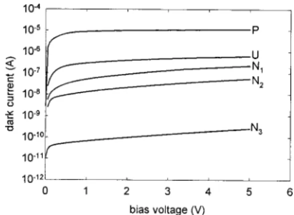
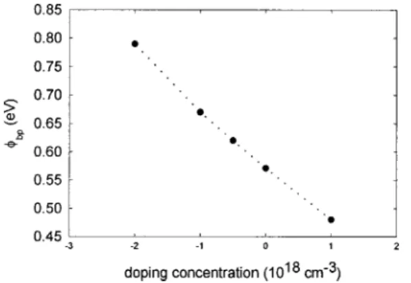
As discussed in the Introduction, if the total current of the MSMPD is dominated by the hole current, we can deter-mine the Schottky barrier height for boles with the total cur-rent easily. The I–V curves of devices T of all five samples are shown in Fig. 4. In the figure we can observe that the current increases slowly with the voltage for all the devices due to the increased image force lowering. From the I–V curves we can extrapolate the total current at zero voltage and then calculate the hole Schottky barrier heights. The Richardson’s constant of holes used in the calculation was 74.4 A/cm2/K2. In Fig. 5 the calculated result is shown. First, it should be noted that the Schottky barrier height for holes of sample U is about 0.57 eV. The summation of this value and the Schottky barrier height for electrons 共0.85 eV兲 is equal to the energy gap of GaAs exactly. This result is not surprising because sample U has an undoped top layer. The Schottky barrier is not modified so the result is consistent
FIG. 3. The measured current–voltage characteristics of the devices T, B, and A of sample N2.
FIG. 4. The measured current–voltage characteristics of the T devices of all the samples: P, U, N1, N2, and N3.
with Eq. 共1兲. This result also indicates the validity of this method for determining the hole Schottky barrier height.
Figure 5 shows that the determined Schottky barrier heights for holes in the range from 0.48 to 0.79 eV were obtained from different samples. Depending on the types of dopants and their doping concentrations, the barrier height can be varied from 0.48 to 0.79 eV. The largest barrier height was obtained when the top layer was n type with a doping concentration of 2⫻1018 cm⫺3. When the top layer was P type with a doping level of 1⫻1018cm⫺3, the barrier height was reduced to 0.48 eV. As shown in the figure, the depen-dence of the barrier height on doping level is nearly linear. The tunable range of the holes Schottky barrier height is comparable to previous reported results and easier to imple-ment due to its good linearity.4 –7 Because the hole barrier height can be greatly increased by the use of a thin n⫹ top layer, the dark current of a MSMPD can be greatly reduced with such a structure. As shown in Fig. 4, the dark current measured from the MSMPD in sample N3 共top layer with a
N-type doping of 2⫻1018 cm⫺3兲 is about three orders of magnitude lower than that measured from the detector on sample U 共the conventional structure兲.
Finally, the responsivities of the devices of all the samples were measured using a commercial 0.85 m laser diode pigtailed with a bare fiber. At an incident power of 25
W, the measured responsivities of all T devices of samples
N1, N2, N3, and U were about 0.12–0.14 A/W under the bias
voltage of 5 V. From this result we can conclude that the
n-type doped top layer, which greatly suppress the dark
cur-rent, does not degrade the responsivity of the devices. The internal quantum efficiencies of the devices were calculated by considering the thickness of the absorption layer, the re-flection from the device surface, and the area of the fingers on the surface. The values were all around 80%.14
III. CONCLUSION
In conclusion we have used the structure of MSMPDs to investigate the modified and unmodified Schottky barrier heights for holes on GaAs. By using a thin and doped top layer, the barrier height can be varied over a wide range. From 1⫻1018 cm⫺3 P-type doping to 2⫻1018cm⫺3n-type
doping the hole barrier height is changed from 0.48 to 0.79 eV. By using the modified barrier height of 0.79 eV we have obtained a reduction in the dark current for over three orders of magnitude for MSM photodetectors.
ACKNOWLEDGMENTS
This work was supported by the National Science Coun-cil under Contract No. NSC 89-2215-E-009-013 and the Lee-MTI Center of National Chiao Tung University.
1C. A. Mead, Solid-State Electron. 9, 1023共1966兲. 2
S. J. Eglash, N. Newman, S. Pan, D. Mo, K. Shenai, W. E. Spicer, F. A. Ponce, and D. M. Collins, J. Appl. Phys. 61, 5159共1987兲.
3S. M. Sze, Physics of Semiconductor Devices, 2nd ed.共Wiley, New York, 1981兲.
4
R. W. Grant and J. R. Waldrop, J. Vac. Sci. Technol. B 5, 1015共1987兲. 5
K. Hirose and E. Foxman, Appl. Phys. Lett. 54, 2347共1989兲.
6K. Hirose, H. Tsuda, and T. Mizutani, Appl. Surf. Sci. 41Õ42, 174 共1989兲. 7S. Fujieda, J. Appl. Phys. 74, 7357共1993兲.
8J. M. Shannon, Solid-State Electron. 19, 537共1975兲. 9
W. E. Stanchina, M. D. Clark, K. V. Vaidyanathan, R. A. Jullens, and C. R. Crowell, J. Electrochem. Soc. 134, 967共1987兲.
10G. P. Schwartz, G. J. Gualtieri, and W. A. Bonner, J. Electrochem. Soc.
133, 1021共1986兲.
11P. Korodosˇ, M. Marso, R. Meyer, and H. Lu¨th, J. Appl. Phys. 72, 2347
共1992兲.
12L. P. Sadwick, C. W. Kim, K. L. Tan, and D. C. Streit, IEEE Electron Device Lett. j12, 626共1991兲.
13S. M. Sze, D. J. Coleman, Jr., and A. Loya, Solid-State Electron. 14, 1209
共1971兲.
14
J. B. D. Soole and H. Schumacher, IEEE J. Quantum Electron. 27, 737
共1991兲.
FIG. 5. The calculated Schottky barrier heights for holes from the result of Fig. 4, where in the axis for doping concentration, the positive side is p type, the negative side is n type, and the zero point is undoped.
5669
J. Appl. Phys., Vol. 90, No. 11, 1 December 2001 S. D. Lin and C. P. Lee