In
fluence of hydrogen plasma treatment on charge storage characteristics in high
density tungsten nanocrystal nonvolatile memory
Shih-Cheng Chen
a, Ting-Chang Chang
b,⁎
, Wei-Ren Chen
c, Yuan-Chun Lo
d, Kai-Ting Wu
d, S.M. Sze
c,
Jason Chen
e, I.H. Liao
e, Fon-Shan Yeh(Huang)
aa
Department of Electrical Engineering & Institute of Electronic Engineering, National Tsing Hua University, Taiwan
b
Department of Physics and Institute of Electro-Optical Engineering, and Center for Nanoscience and Nanotechnology, National Sun Yat-Sen University, Taiwan
c
Institute of Electronics, National Chiao Tung University, Hsin-Chu, Taiwan
d
Institute Photonics of Technologies National Tsing Hua University, Taiwan
eProMOS Technologies, No. 19 Li Hsin Rd., Science-Based Industrial Park, Hsinchu, Taiwan
a b s t r a c t
a r t i c l e i n f o
Article history: Received 14 July 2010
Received in revised form 12 January 2011 Accepted 14 January 2011
Available online 27 January 2011 Keywords:
Hydrogen plasma Tungsten nanocrystals Nonvolatile memory
X-ray photoelectron spectroscopy
This study focuses on the influence of a hydrogen plasma treatment on electrical properties of tungsten nanocrystal nonvolatile memory. The X-ray photon emission spectra show that, after the hydrogen plasma treatment, a change in binding energy occurs such that Six+and Siy+peaks appear at a position that is shifted about 2.3 and 3.3 eV from Si0+in Si 2p spectra. This indicates that Si dangling bonds are passivated to form a Si–H bond structure in the SiO2. Furthermore, the transmission electron microscopy shows cross-sectional and plane-view for the nanocrystal microstructure after the hydrogen plasma treatment. Electrical measurement analyses show improved data retention because the hydrogen plasma treatment enhances the quality of the oxide surrounding the nanocrystals. The endurance and retention properties of the memory device are improved by about 36% and 30%, respectively.
© 2011 Elsevier B.V. All rights reserved.
1. Introduction
Conventional nonvolatile memory (NVM, flash memory) suffers from certain limitations during continual scaling of device structures[1]. Therefore, in recent years nanocrystal (NC) nonvolatile memory devices have been investigated as a method to overcome these drawbacks. Because discrete trap storage nodes act as the charge center of NC nonvolatile memory devices, they can effectively avoid data loss in terms of reliability when scaling down such devices[2].
Among various NC nonvolatile memories [3–5], metal NCs are good candidates for improving the retention property and charge storage ability[6]due to their high work function, which provides a lower potential well compared to the silicon substrate. Tungsten (W) NC was chosen because, besides its high work function (4.9 eV), thermal stability is suitable for the process thermal budget [7–9]. Moreover, for nanoscale devices, the density of nanocrystals is an issue because the memory window is dependent on the NC density. High density is helpful to scale down the device structure. However, if the density of NCs is very high, then the quality of the oxide which surrounds the NCs will be critical because the electrons stored in NCs will escape easily by trap tunneling if the oxide quality is not sufficient. When NCs are very close to each other[10,11], there is a
tradeoff between high NC density and good reliability for nano-NVM application. In order to achieve both high density and good reliability, using high-pressure hydrogen treatment with high temperature annealing (700–900 °C) has proven to be a valid method to improve the oxide surrounding NCs [12,13]. Unfortunately, metal NCs and metal control gates cannot endure this temperature treatment. Hence, a hydrogen plasma treatment is proposed for W NC nonvolatile memory as an alternative method to passivate the defects in the surrounding oxide and improve its quality. The advantages of this method are a simple fabrication process and a low thermal budget. 2. Experiment
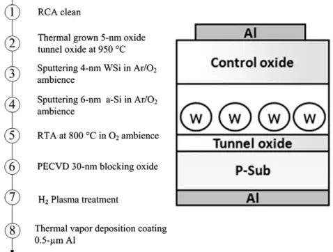
The processflow and the memory structure for this study are shown inFig. 1. The W NC NVM capacitor structure was fabricated on single-crystal 6 in. (100) oriented P-type silicon. After the standard RCA cleaning, wafers went through a thermal oxidative process in an atmospheric pressure chemical vapor deposition furnace to form a 5 nm thick dry SiO2layer that serves as a tunnel oxide. Afterward, a
4 nm thick tungsten silicide (WSi2) thinfilm was deposited onto the
tunnel oxide by sputtering at room temperature with argon plasma 50 sccm (sccm denotes cubic centimeter per minute at standard temperature and pressure) and a DC power of 100 W. Subsequently, a 6 nm thick amorphous silicon (a-Si) layer was deposited by the same system with argon plasma 30 sccm and a RF power of 100 W. After the deposition of this WSi2/a-Si double layer structure, high temperature
Thin Solid Films 519 (2011) 3897–3901
⁎ Corresponding author. Tel.: +886 7 5252000x3708; fax: +886 7 5253709. E-mail address:[email protected](T.-C. Chang).
0040-6090/$– see front matter © 2011 Elsevier B.V. All rights reserved. doi:10.1016/j.tsf.2011.01.259
Contents lists available atScienceDirect
Thin Solid Films
thermal oxidation was performed in the Rapid Thermal Annealing (RTA) system in oxygen ambient. RTA oxidation at 800 °C for 60 s is required to allow the WSi2layer to form W NCs, which then embed
between the tunnel oxide and the control oxide. Afterwards, a 30 nm thick SiO2layer was deposited by a plasma enhanced chemical vapor
deposition system to form a control oxide layer. For comparison, some of the samples were treated with hydrogen plasma for 30 min by high density plasma chemical vapor deposition at 200 W of plasma power and 200 sccm gas flow rate at 300 °C. The standard sample was plasma treated, whereas the control sample was used as reference without treatment, and will be referred to as standard and control samples hereafter. Finally, the top and the bottom Al electrodes were patterned by a shadow mask to form a metal–oxide–insulator–oxide– silicon structure. The aluminum was deposited by a thermal evapo-rator system with a thickness of 500 nm. Transmission electron microscope (TEM) analysis and X-ray photoelectron spectroscopy (XPS) were adopted for the microstructure and the chemical material analyses of nanoparticles. The cross-sectional TEM sample was prepared by focused ion beam process using a SII Nanotechnology Incorporated SMI 3050 system. The plane-view TEM sample was prepared byfirst polishing the sample thickness down to around 100μm with a grinding polishing machine. Then the sample thickness is further reduced to about 10μm by milling with Ar+
ions using a Gatan Model 691 precise ion polishing system. The high-resolution TEM was carried out using a JEOL JEM-2100F system operated at 200 kV. XPS analysis was performed using a VG Scientific Microlab 310F with 300 W Al Kα (1486.6 eV) as the X-ray source and was calibrated by a C 1s peak at 284.5 eV. The functions used for decon-volution are naturally broad and can be approximated with finite Gaussian or Lorentzian shape or a combination by XPSPEAK41 software. The electrical characteristics of capacitance–voltage (C–V) hysteresis were also measured by an HP4284 Precision LCR Meter with a high frequency of 100 kHz.
3. Results and discussion
Fig. 2(a) and (b) shows the TEM image cross-sectional and plane-view for the proposed device. The TEM image analyses show that the
average diameter of nanocrystals is approximately 8 nm and the area density can be estimated to be about 2.5 × 1012cm− 2. After going
through the process indicated above, a high density of NCs was gained appropriate for 32–22 nm device applications.
Fig. 3(a) and (b) shows the Si 2p spectra of the control and standard sample, performed by a monochromatic Al Kα (1486.6 eV) X-ray. InFig. 3(a), the transition region spectra between Si0+and Si4+ are not observed in the SiO2, which had not been exposed to the
hydrogen plasma. Therefore, deconvolution of the spectra was carried out assuming that only Si0+and Si4+peaks exist in the Si 2p spectra for the unexposed SiO2[14–17]. In contrast, the SiO2which had been
exposed to the hydrogen plasma exhibited transition region spectra between Si0+and Si4+in the Si 2p spectra, shown inFig. 3(b). These
transition region spectra could not be deconvoluted as Si3+, Si2+and
Si1+. It has been reported that Six+and Siy+ spectra which have
shifted about 2.3 and 3.3 eV from Si0+will appear in Si 2p spectra if a
Si–H bond structure exists in the SiO2. Therefore, because our results
exhibit just such transition spectra, the sample with hydrogen plasma treatment can be assumed to produce the Si–H bonding and chemical shifts for Si–H bonding configurations, as shown inFig. 3(c). In addi-tion, the shift to lower energy and the increase in the intensity of the Si0+peak and the presence of the Si2+after hydrogen plasma
treat-ment are caused by the Si and Si–Si2O2reduction from weak Si– O4
bonds[18–20]. Moreover, W 4f core-level photoemission spectra of the control and standard samples both consist of the two main peaks of W 4f7/2(31.4 eV) and W 4f5/2(33.5 eV), as shown inFig. 4(a) and
(b). The small peak at a position 35.2 eV is the peak of WO3of W 4f
bonding[21,22]. Some of the W was probably oxidized during the rapid thermal annealing in the oxygen ambient because the solid solubility of O atoms within W material is extremely small[23], and O atoms cannot exist in W nanocrystals except if there is absolute oxidation of tungsten. Therefore, the position of WO3will be on the
surface of the W nanocrystals. The W 4f spectra of the control and standard sample are very similar. In addition, in our experiment, the hydrogen plasma treatment is a post-treatment after the W nanocrystal formation. Therefore, it is unlikely that the W 4f spectra of the control and standard sample would show major differences, as the treatment does not influence the W nanocrystal formation. Fig. 1. Processflow and W nanocrystal NVM structure.
As the C–V hysteresis diagram inFig. 5shows, the memory window is ~8.8 V under ±10 V compared to theflat-band gate voltage operation. This memory window is sufficient to define the digital data information “1” and “0” for low power nano-NVM applications. Moreover, hysteresis loops follow a counterclockwise direction due to the injection of electrons from the inversion state and the discharge of electrons from the accumulation state of the Si substrate. The memory window of the standard sample that had the plasma treatment is slightly larger than the control sample under the same operation voltage. Hence, the charge storage ability of W NC NVMs is not influenced by the post-hydrogen plasma treatment in the standard sample. This shows that, for metallic NCs, most of the efficacious electron store in the W NCs rather than the surrounding oxide defects. In general, the memory window decreases as the trap density is reduced in SONOS-type memory. However, in nanocrystal memory, because charges are mainly stored in nanocrystals,
there is no obvious variation in the memory window as the device is treated by hydrogen plasma treatment. The slight increase of memory window suggests that the improvement of oxide quality surrounding the nanocrystals suppresses de-trapping via traps. In addition, the Si nanocrystals formed during the hydrogen plasma treatment can provide additional storage states.
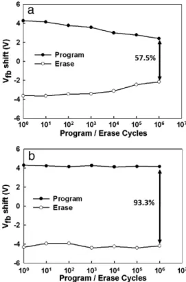
Fig. 6(a) and (b) presents the endurance characteristics of control and standard samples under the pulse condition of VG−Vfb= ±7 V
for 10 ms. Theflat-band voltage (Vfb) shift can be defined by using the
C–V hysteresis under ±7 V gate voltage operation. The memory of control samples can be distinguished after 106program/erase cycles
at room temperature; however, memory is degraded to about 57.5%, as shown inFig. 6(a). This is because during the endurance test, carrier transport between nanocrystals and the substrate can damage the surrounding oxide.
Fig. 3. XPS analysis of the Si 2p core-level spectrum. (a) Control sample, (b) standard sample, and (c) Si–H bond structure in the SiO2and theoretical chemical shifts calculated by the
concept of local electronegativity.
Fig. 2. TEM image of W nanocrystal NVM. (a) Cross-section, and (b) plane-view.
3899 S.-C. Chen et al. / Thin Solid Films 519 (2011) 3897–3901
Fig. 6(b) shows that the variation of the memory window is stable (△VFBof 93.3%) after 106program/erase cycles for devices with the
hydrogen plasma treatment. It is known that the△VFBreduction during
the endurance test is due to the degradation of the gate oxide[24]. The superior endurance characteristics of the sample with hydrogen plasma treatment can be attributed to the improvement of surrounding oxide quality. The surrounding oxide was strengthened by the hydrogen incorporation after the treatment; therefore, the generation rate of traps is reduced, resulting in better endurance properties.
Fig. 7shows the retention characteristics of the W NC nonvolatile memory. The open triangles represent the standard sample, and the solid black circles represent the control sample. We used an extrapolation to give a long-term predictable result (dotted lines) after 1000 s (stable region of retention). The memory window signi-ficantly decays during the first 100 s due to the charge emission from the shallow traps in SiOx matrix to the substrate. However, after 100 s the memory window becomes more stable. A 1.39 V memory window (charge ratio remaining at 69.4%) can be obtained after 104s. As
shown inFig. 6, the retention property of the sample with hydrogen plasma treatment is superior. The better retention characteristics of the sample with the plasma treatment can be attributed to the improvement of surrounding oxide quality.
As the density of NCs increases, the oxide surrounding those NCs becomes very thin. If the surrounding oxide quality is not sufficient, it will be unable to block the lateral electron migration effect, and the electron storage in the NCs will escape, as shown inFig. 8(a). The hydrogen plasma treatment can be used to effectively passivate dangling bonds of the Si/SiO2interface and defects in the surrounding
oxide such that Si–H bonds are formed. Hence, the lateral electron migration will be reduced, as shown inFig. 8(b).
4. Conclusion
This study investigates the influence of hydrogen plasma treatment on the electrical characteristics and the chemical composition of the proposed W nanocrystal nonvolatile memory. After the hydrogen plasma treatment, the XPS results indicate that Si dangling bonds (traps) in SiO2have been repaired by hydrogen passivation and have
Fig. 5. Capacitance–voltage (C–V) hystereses of MOIOS structure with W nanocrystal NVM under ±10 V gate voltage operation.
Fig. 6. Endurance characteristics of (a) control sample and (b) standard sample under the pulse condition of VG−VFB= ± 7 V for 10 ms. Theflat-band voltage can be defined
by using the C–V hysteresis.
Fig. 7. Retention of the nonvolatile W nanocrystal NVM. Fig. 4. XPS analysis of the W 4f core-level spectrum. (a) Control sample, and
formed a H-passivated bonding (Six+and Siy+). In addition, the binding
energy reduction and the increased intensity of the Si0+peak reveal that
Si nanocrystals form due to the Si reduction from weak Si–O bonds during hydrogen plasma treatment. Because Si nanocrystals can provide additional storage centers, the memory window increases slightly, even though traps were passivated. By using the hydrogen plasma treatment, the endurance and retention properties of the memory device can be improved by 36% and 30%, respectively. The reason the reliability improved was that Si dangling bonds were repaired to form Si–H bonds during hydrogen plasma treatment. In addition, the process is compatible with currentflash memory fabrication technology. Acknowledgements
This work was performed at the National Science Council Core Facilities Laboratory for Nano-Science and Nano-Technology in Kaohsiung–Pingtung area and supported by the National Science Council of the Republic of China under Contract Nos. NSC-99-2120-M-110-001 and NSC 97-2112-M-110-009-MY3.
References
[1] H.E. Maes, J. Witter, G. Groeseneken, Proc. 17 European Solid State Devices Res. Conf. Bologna (1998) 157.
[2] S. Tiwari, F. Rana, K. Chan, H. Hanafi, C. Wei, D. Buchanan, IEEE Int. Electron Devices Meet Tech. Dig. (1995) 521.
[3] Chao-Cheng Lin, Ting-Chang Chang, Tu. Chun-Hao, Wei-Ren Chen, Hu. Chih-Wei, Simon M. Sze, Tseung-Yuen Tseng, Sheng-Chi Chen, Jian-Yang Lin, Appl. Phys. Lett. 93 (2008) 222101.
[4] Wei-Ren Chen, Ting-Chang Chang, Jui-Lung Yeh, Chun-Yen Chang, Shih-Ching Chen, Appl. Phys. Lett. 92 (2008) 062112.
[5] Wei-Ren Chen, Ting-Chang Chang, Jui-Lung Yeh, Simon M. Sze, Chun-Yen Chang, Uei-Shin Chen, Appl. Phys. Lett. 91 (2007) 222105.
[6] H.G. Yang, Y. Shi, S.L. Gu, B. Shen, P. Han, R. Zhang, Y.D. Zhang, Microelectron. J. 34 (2003) 71.
[7] C.H. Chen, T.C. Chang, I.H. Liao, P.B. Xi, Joe Hsieh, Chen Jason, Huang Tensor, S.M. Sze, U.S. Chen, J.R. Chen, Appl. Phys. Lett. 92 (2008) 013114.
[8] S.K. Samanta, Zerlinda Y.L. Tan, Won Jong Yoo, Ganesh Samudra, Sungjoo Lee, L.K. Bera, N. Balasubramanian, JVST B 23 (6) (2005) 2278.
[9] Jer-Chyi Wang, Pai-Chi Chou, Chao-Sung Lai, Wen-Hui Lee, Chi-Fong Ai, Microelectron. Reliab. 50 (2010) 639.
[10] M. Houssa, M. Tuominen, M. Naili, V. Afanas'ev, A. Stesmans, S. Haukka, M.M. Heyns, J. Appl. Phys. 87 (2000) 8615.
[11] W.R. Chen, T.C. Chang, P.T. Liu, P.S. Lin, C.H. Tu, C.Y. Chang, Appl. Phys. Lett. 90 (2007) 112108.
[12] G. Taraschi, S. Saini, W.W. Fan, L.C. Kimerling, J. Appl. Phys. 93 (2003) 9988. [13] C.H. Tu, T.C. Chang, P.T. Liu, H.C. Liu, S.M. Sze, C.Y. Chang, Appl. Phys. Lett. 89
(2006) 162105.
[14] T. Suzuki, M. Muto, M. Hara, K. Yamabe, T. Hattori, Jpn. J. Appl. Phys. 25 (1986) 544.
[15] A. Ikeda, T. Sadou, H. Nagashima, K. Kouno, N. Yoshikawa, K. Tshukamoto, Y. Kuroki, Thin Solid Films 345 (1999) 172.
[16] Kazuhisa Sugiyama, Takayuki Igarashi, Kazunori Moriki, Yoshikatsu Nagasawa, Takayuki Aoyama, Rinshi Sugino, Takashi Ito, Takeo Hattori, Jpn. J. Appl. Phys. 29 (1990) L2401.
[17] T. Hattori, T. Igarashi, M. Ohi, H. Yamagishi, Jpn. J. Appl. Phys. 28 (1989) L1436. [18] Yasushi Sawada, Noriyuki Taguchi, Kunihide Tachibana, Jpn. J. Appl. Phys. 38
(1999) 6506.
[19] Chung-Jin Kim, Sung-Jin Choi, Seong-Wan Ryu, Sungho Kim, Jae-Joon Chang, SuHak Bae, Byeong-Hyeok Sohn, Yang-Kyu Choi1, Nanotechnology 21 (2010) 125202.
[20] T.P. Nguyen, S. Lefrant, Phys. Condens. Matter (1989) 5197. [21] L.G. Piper, W.T. Rawlins, J. Chem. Phys. 90 (1986) 320. [22] R. Wolf, K. Wandel, Surf. Coat. Technol. 74 (75) (1995) 522.
[23] O. Kubaschewski, B.E. Hopkins, Oxidation of Metals and Alloys, Butterworths, London, 1953.
[24] P. Pavan, R. Bez, P. Olivo, E. Zanoni, Proc. IEEE 85 (1997) 1248. Fig. 8. (a) Lateral leakage current phenomenon of non-ideal NC structure. (b) NC structure with plasma treatment.
3901 S.-C. Chen et al. / Thin Solid Films 519 (2011) 3897–3901