Interfacial reactions of Pt-based Schottky contacts on InGaP
L. H. Chu, E. Y. Chang, Y. H. Wu, J. C. Huang, Q. Y. Chen, W. K. Chu, H. W. Seo, and C. T. Lee
Citation: Applied Physics Letters 92, 082108 (2008); doi: 10.1063/1.2834849 View online: http://dx.doi.org/10.1063/1.2834849
View Table of Contents: http://scitation.aip.org/content/aip/journal/apl/92/8?ver=pdfcov Published by the AIP Publishing
Articles you may be interested in
Correlating the Schottky barrier height with the interfacial reactions of Ir gates for In Al As In Ga As high electron mobility transistors
Appl. Phys. Lett. 89, 211910 (2006); 10.1063/1.2393005 Schottky barrier characteristics of Pt contacts to n -type InGaN J. Appl. Phys. 99, 073704 (2006); 10.1063/1.2187274
Influence of thermal oxidation on the electronic properties of Pt Schottky contacts on GaN grown by molecular-beam epitaxy
Appl. Phys. Lett. 86, 083507 (2005); 10.1063/1.1868863 Properties of Cu/Au Schottky contacts on InGaP layer J. Appl. Phys. 94, 3805 (2003); 10.1063/1.1602574
Microstructure evolution and failure mechanism for Cu/Au Schottky contacts to InGaP layer J. Appl. Phys. 92, 987 (2002); 10.1063/1.1487439
This article is copyrighted as indicated in the article. Reuse of AIP content is subject to the terms at: http://scitation.aip.org/termsconditions. Downloaded to IP: 140.113.38.11 On: Wed, 30 Apr 2014 23:14:26
Interfacial reactions of Pt-based Schottky contacts on InGaP
L. H. Chu,a兲 E. Y. Chang,b兲 Y. H. Wu, and J. C. Huang
Department of Materials Science and Engineering, National Chiao-Tung University, Hsinchu 30050, Taiwan, Republic of China
Q. Y. Chenc兲 and W. K. Chu
Department of Physics and Texas Center for Superconductivity, University of Houston, Houston, Texas 77204, USA
H. W. Seo
Department of Physics, University of Arkansas, Little Rock, Arkansas 72204, USA
C. T. Lee
Institute of Microelectronics, National Cheng-Kung University, Tainan 70101, Taiwan, Republic of China
共Received 7 March 2007; accepted 3 December 2007; published online 28 February 2008兲 We have investigated the interfacial reaction between platinum and InGaP in a Schottky diode structure. There was a 7.5-nm-thick amorphous layer formed at the interface between Pt and InGaP after metal deposition. After annealing at 325 ° C for 1 min, this amorphous layer increased to 12.8 nm and the reverse leakage current also decreased. The diffusion of Pt atoms and the crystallization of amorphous layer took place after annealing at 325 ° C for 10 min. Prolonging the annealing to 3 h led to formation of Ga2Pt and GaPt3phases in InGaP and Schottky diodes degraded
after these new phases were observed. © 2008 American Institute of Physics. 关DOI:10.1063/1.2834849兴
Aluminum-free InGaP semiconductor on GaAs has re-cently attracted a great deal of attention because of its microwave-device application possibilities.1–5 InGaP has an edge over conventional AlGaAs for its wider band gap, high etching selectivity, low surface recombination velocity, less susceptibility to surface oxidation, and the absence of DX centers.6In the past few years, interfacial reactions of vari-ous Schottky-contact metals, such as Pt/Ti/Pt/Au,5 Ti/Pt/Au,7,8
WSiN,9 and Cu/Au,10–12 with the InGaP have been extensively studied, but none were proven perfect for technological implementations. The Schottky-contact quali-ties of InGaP/Ti/Pt/Au7
and InGaP/WSiN,8 for example, were found to degrade after a 500 ° C heat treatment at
which spurious CuP2 for InGaP/Cu/Au has also been
reported.12
In seeking solutions to surmount such interface-reaction problems, Pt has lately been used as a gate-sinking metal to keep the threshold voltage and leakage current under control for InGaP high electron mobility transistor devices4because of their higher Schottky barrier which could translate directly into reduced leakage current and thus also enhanced device performance.5,13Unfortunately, Nebauer et al.3has observed GaPtx compounds and other multicomponent phases while
Ga2Pt compound has also been detected using x-ray
diffractometry4in the annealed Pt/InGaP junctions. Whether Pt can be an enabling Schottky metal or not would hence depend on how resilient it is to the thermal processing with-out interacting with the semiconductor. Nevertheless, the ex-act nature of this interface reex-action remains unclear. This is possibly due to the difficulty in properly labeling Ga atoms
in the InGaP/GaAs heterostructure and the lack of clear electron diffraction patterns necessary to help determine the zone axis of the InGaP semiconductor layer. There is thus an incentive to continue to better understand the Pt/InGaP in-terface properties to help shed some light on why Pt/Ti/Pt/Au metals fail as a good Schottky contact and whether a solution to can be found to prevent it.
In this work, the material stability and the interfacial reactions between Pt and InGaP were analyzed with high resolution transmission electron microscopy共HRTEM兲 while the current-voltage characteristics of Pt/InGaP Schottky di-odes were also measured to seek correlations between the material structures and device performances. The hetero-structure consists of, from bottom to top, a GaAs buffer layer, a 200 Å thick undoped In0.49Ga0.51P Schottky layer,
and a 750 Å thick heavily doped n+-GaAs cap layer. The
Schottky diode schematics were shown in Fig. 4 and fabri-cated by following steps: firstly, the Ohmic metal-contact metals Au/Ge/Ni/Au were deposited on the cap layer in sequence, and subsequently, the samples were annealed at 350 ° C for 1 min to minimize the contact resistance. The
a兲NSC GSSAP Research Fellow, also with Texas Center for Superconduc-tivity, University of Houston, Houston, Texas, USA.
b兲Electronic mail: [email protected].
c兲Also with Dept of Physics and Center for Nanoscience and Nanotechnol-ogy, National Sun Yat-Sen University, Taiwan.
FIG. 1. 共a兲 The cross-sectional HRTEM image of Pt and InGaP interface after metal deposition.共b兲 The cross-sectional HRTEM image of the Pt and InGaP interface after annealing at 325 ° C for 1 min.
APPLIED PHYSICS LETTERS 92, 082108共2008兲
0003-6951/2008/92共8兲/082108/3/$23.00 92, 082108-1 © 2008 American Institute of Physics
This article is copyrighted as indicated in the article. Reuse of AIP content is subject to the terms at: http://scitation.aip.org/termsconditions. Downloaded to IP: 140.113.38.11 On: Wed, 30 Apr 2014 23:14:26
contact resistance 共Rc兲 was measured via the transmission
line model 共TLM兲 method using 100m 共Wx兲⫻75m
共Wy兲 pads with interedge spacing of the neighboring pads 共L兲 ranging from 36, 20, 10, 5, to 3m sequentially. The total resistance R共L兲=2Rc+ Rs, where Rs is the resistance of the sample of length L, width Wy and thickness t, and RS =sL/tWy. The sample sheet resistance Rsheet=s/t hence
R共L兲=2Rc+ RsheetL/Wy. Hence, one can obtain R共0兲=2Rcby extrapolating the supposedly linear relation to L = 0 to find the intercept of the R axis, while the slope represents
Rsheet/Wy. Meanwhile, from the L-axis intercept R共2Lt兲=0, one obtains Lt= −RcWy/Rsheet. Both Rcand the sample sheet resistance Rsheetof the semiconductor being measured follow
naturally once the two intercepts are known. In the TLM method, all the voltage drops from the pads to the sample are assumed to be across the two neighboring edges of the pads on which the electrodes are placed共thus only Wyis relevant, but not Wx兲. With this in mind, we have Rc= 2.56⍀, Lt=
−1.06m, and Rsheet= 180⍀/䊐 for the InGaP. These give the figure of merit RcWy= 0.19⍀ mm, as compared to the previously reported 0.14⍀ mm in Ref. 4for a device struc-ture of similar materials though somewhat differently config-ured, where the associated numbers are Wy= 75m, Rc = 1.93⍀, Lt= −1.18m, and Rsheet= 123⍀/䊐 for the InGaP.
The Schottky electrode consists of Au 共300 nm兲/Pt 共100 nm兲/Ti 共100 nm兲/Pt 共20 nm兲 stack, placed directly on InGap after the n+GaAs layer was removed by a citric-acid/ H2O/H2O2solution, all by e-beam evaporation. The 300 nm
Au layer serves to lower the overall Schottky-metal resis-tance while the 100 nm Pt layer acts a diffusion barrier to prevent Au from diffusing into the Au/Pt/Ti/Pt/InGaP Schottky diode structure,14largely because of its high melt-ing point and compatibility with the lift-off process. Note that in order to optimize the Schottky barrier height,5placed at the bottom of the metal stack is a 20 nm layer of Pt sepa-rated from the other 100 nm Pt layer by an also 100 nm thick Ti layer. Finally, these Schottky diodes were annealed, for various durations at 325 ° C, which is 25 ° C below Ohmic annealing temperature, avoiding affecting Ohmic contact resistance.
Energy dispersive x-ray 共EDX兲 with electron beam of 2 nm spot size equipped on a HRTEM was performed for composition analysis. The HRTEM image showing the Pt/InGaP interface for an as-deposited sample is presented in Fig.1共a兲. Each layer was identified by the nanobeam EDX analysis. As is obvious, there is a 7.5 nm thick amorphous layer existing at the Pt/InGaP interface and similar results were also found in the as-deposited Pt/GaAs interfaces15 even for samples as-deposited at room temperature. The amorphous phase formation implicates the enormous inher-ent thermodynamic driving forces15that push the Pt atoms to migrate into the InGaP layer. After annealing at 325 ° C for 1 min, the thickness of the amorphous layer increased from 7.5 to 12.8 nm. The diminution of the InGaP layer is due to the fact that more Pt atoms diffused into the pristine InGaP layer after thermal annealing. The diffusion boundary be-tween InGaP and the amorphous layer was nonuniform, which could be caused by the nonuniform thermal process due to the short-time annealing.
Figure 2 共a兲 shows the HRTEM image of the Pt and
InGaP interface reaction, whereas Fig.2共c兲gives the selected area diffraction patterns of the amorphous layer after 325 ° C annealing for 10 min. Nucleation of crystalline phase oc-curred in the amorphous layer after annealing for 10 min at FIG. 2.共a兲 The cross-sectional HRTEM image of the Pt and InGaP interface
after annealing at 325 ° C for 10 min.共b兲 The fast Fourier transform 共FFT兲 lattice image of the amorphous area which was shown in共a兲. The nucleation area was labeled by white square.共c兲 Nanobeam selected area electron dif-fraction pattern of the amorphous area shown in2共a兲.
FIG. 3.共a兲 The cross-sectional HRTEM image of the Pt and InGaP interface after 325 ° C annealing for 3 h and nanobeam selected area diffraction pat-tern showing the Ga2Pt共422兲 phase. 共b兲 The cross-sectional HRTEM image of Pt and InGaP interface after 325 ° C annealing for 3 h and nanobeam selected area diffraction pattern showing the GaPt3共422兲 phase.
082108-2 Chu et al. Appl. Phys. Lett. 92, 082108共2008兲
This article is copyrighted as indicated in the article. Reuse of AIP content is subject to the terms at: http://scitation.aip.org/termsconditions. Downloaded to IP: 140.113.38.11 On: Wed, 30 Apr 2014 23:14:26
325 ° C, as shown in Fig.2共b兲. The HRTEM image of the InGaP/GaAs interface after annealing at 325 °C for 3 h is provided in Fig.3共a兲. The crystalline grains were observed in the amorphous layer near its interface with InGaP and were identified as an orthorhombic Ga2Pt 共422兲 phase, judged
from the nanobeam selected area diffraction patterns. The HRTEM image of the Pt/InGaP interface after annealing at 325 ° C for 3 h is presented in Fig.3共b兲. However, near the interface of the amorphous layer with Pt, a tetragonal GaPt3
共422兲 phase was observed. On the basis of these observa-tions, this thin amorphous layer, it can be concluded, could be a precursory step to forming more stable Ga2Pt共422兲 and
GaPt3共422兲 phases at the later stage of annealing. The new phases of the Ga2Pt共422兲 and GaPt3共422兲 existed in
differ-ent locations of the amorphous layer. The Ga2Pt 共422兲 near
the InGaP layer was a result of the outdiffusion of Ga from InGaP into the amorphous layer, and GaPt3 共422兲 was
present near the alloy-Pt interface.
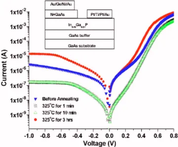
Figure4 shows the I-V characteristics of the diodes be-fore and after annealing, the leakage current decreased after 325 ° C, 1 min annealing, possibly due to Pt diffusion.16 Af-ter 325 ° C annealing for 10 min, the diodes’ performance remained almost unchanged even with the crystalline phase nucleated in the amorphous layer as shown in Fig.2共b兲. In summary, the interfacial reactions between the Pt and the InGaP layer after thermal annealing has been investigated. A 7.5 nm-thick amorphous layer was formed between Pt and InGaP layer after the room-temperature gate-metal deposi-tion. After annealing at 325°C for 10 minutes,
crystalliza-tions took place in the amorphous layer. At this stage, the thickness of amorphous layer remained unchanged; indicat-ing that insertion of the Ti layer was effective as a diffusion barrier at 325°C. After annealing for 3 hours at 325 ° C, however, stable phases of Ga2Pt 共422兲 and GaPt3 共422兲 formed in the InGaP layer, though not in the Schottky metal stack, leading to degradation of the diode performances. However, the Ga2Pt共422兲 phase was observed at the InGaP/ GaAs interface, exhibiting continuing diffusion of Pt atoms beyond the 3-hour annealing. Thus, further study on the Pt diffusion at various annealing temperatures and durations for the contact metal stacks with, for example, thinner bottom Pt layers may be necessary to optimize the Schottky character-istics stabilization.
The authors would like to acknowledge the support from the National Science Council, and the Ministry of Economic Affairs, Taiwan, R.O.C., under the Contracts Nos. NSC 95-2752-E-009-001-PAE and 95-EC-17-A-05-S1-020. The work at Houston was supported in part by the U.S. National Sci-ence Foundation through Grant No. DMR-0404542, the U.S. Department of Energy through Grant No. DE-FG02-05ER46208, the U.S. Air Force Office of Scientific Research through Grant No. FA9550-06-1-0401, and the State of Texas Strategic Partnership for Research in Nanotechnology 共SPRING兲 through the Texas Center for Superconductivity at the University of Houston.
1P. Fay, K. Stevens, J. Elliot, and N. Pan, IEEE Electron Device Lett. 20, 554共1999兲.
2Y. C. Lin, E. Y. Chang, H. M. Lee, and C. Y. Chang, Electron. Lett. 40, 777共2004兲.
3E. Nebauer, M. Mai, J. Wurfl, and W. Osterle, Semicond. Sci. Technol.
15, 818共2000兲.
4L. H. Chu, E. Y. Chang, L. Chang, Y. H. Wu, S. H. Chen, H. T. Hsu, T. L. Lee, Y. C. Lien, and C. Y. Chang, IEEE Electron Device Lett. 28, 82 共2007兲.
5J. R. Lothian, F. Ren, J. M. Kuo, J. S. Weiner, and Y. K. Chen, Solid-State Electron. 41, 673共1997兲.
6M. O. Watanabe and Y. Ohba, J. Appl. Phys. 60, 1032共1986兲. 7C. T. Lee, H. P. Shiao, N. T. Yeh, C. D. Tsai, Y. T. Lyu, and Y. K. Tu,
Solid-State Electron. 41, 1共1997兲.
8C. T. Lee, M. H. Lan, and C. D. Tasi, Solid-State Electron. 41, 1715 共1997兲.
9K. Shiojima, K. Nishimura, and F. Hyuga, J. Vac. Sci. Technol. B 14, 652 共1996兲.
10D. S. Liu, C. T. Lee, and C. W. Wang, J. Appl. Phys. 94, 3805共2003兲. 11D. S. Liu and C. T. Lee, J. Appl. Phys. 91, 1349共2002兲.
12D. S. Liu and C. T. Lee, J. Appl. Phys. 92, 987共2002兲.
13P. Fay, K. Stevens, J. Elliot, and N. Pan, IEEE Electron Device Lett. 20, 554共1999兲.
14G. Stareev, H. Kunzel, and G. Dortmann, J. Appl. Phys. 74, 7344共1993兲. 15C. Fontaine, T. Okumura, and K. N. Tu, J. Appl. Phys. 54, 1404共1983兲. 16S. Kim, I. Adesida, and H. Hwang, Appl. Phys. Lett. 87, 232102共2005兲. FIG. 4.共Color online兲 I-V characteristics of the Schottky diodes before and
after annealing.
082108-3 Chu et al. Appl. Phys. Lett. 92, 082108共2008兲
This article is copyrighted as indicated in the article. Reuse of AIP content is subject to the terms at: http://scitation.aip.org/termsconditions. Downloaded to IP: 140.113.38.11 On: Wed, 30 Apr 2014 23:14:26