Investigation on multilayered chemical vapor deposited Ti/TiN films as the diffusion
barriers in Cu and Al metallization
J. C. Hu, T. C. Chang, L. J. Chen, Y. L. Yang, S. Y. Chen, and C. Y. Chang
Citation: Journal of Vacuum Science & Technology A 17, 2389 (1999); doi: 10.1116/1.581777 View online: http://dx.doi.org/10.1116/1.581777
View Table of Contents: http://scitation.aip.org/content/avs/journal/jvsta/17/4?ver=pdfcov
Published by the AVS: Science & Technology of Materials, Interfaces, and Processing
Articles you may be interested in
The role of barrier layer on Ohmic performance of Ti Al -based contact metallizations on Al Ga N Ga N heterostructures
J. Appl. Phys. 100, 023708 (2006); 10.1063/1.2218766
Strengthening TiN diffusion barriers for Cu metallization by lightly doping Al
Appl. Phys. Lett. 87, 121911 (2005); 10.1063/1.2056583
Optimization of Al interlayer thickness for the multilayer diffusion barrier scheme in Cu metallization
J. Appl. Phys. 92, 1099 (2002); 10.1063/1.1486039
TiSiN films produced by chemical vapor deposition as diffusion barriers for Cu metallization
J. Vac. Sci. Technol. B 20, 1471 (2002); 10.1116/1.1494068
Ti, TiN, and Ti/TiN thin films prepared by ion beam assisted deposition as diffusion barriers between Cu and Si
as the diffusion barriers in Cu and Al metallization
J. C. Hu
Department of Materials Science and Engineering, National Tsing Hua University, Hsinchu, Taiwan, Republic of China
T. C. Changa)
National Nano Device Laboratory, Hsinchu, Taiwan, Republic of China and Department of Physics, National Sun Yat-Sen University, Kaohsiung, Taiwan, Republic of China
L. J. Chen
Department of Materials Science and Engineering, National Tsing Hua University, Hsinchu, Taiwan, Republic of China
Y. L. Yang
National Nano Device Laboratory, Hsinchu, Taiwan, Republic of China
S. Y. Chen
Department of Electrical Engineering, National Tsing Hua University, Hsinchu, Taiwan, Republic of China
C. Y. Chang
Department of Electronics Engineering and Institute of Electronics, National Chiao Tung University, Hsinchu, Taiwan, Republic of China
~Received 13 October 1998; accepted 22 February 1999!
A novel multilayered chemical vapor deposition ~CVD! Ti/TiN structure was found to be a more effective diffusion barrier in Cu metallization than TiN alone. The Ti and TiN films were deposited by plasma enhanced CVD and low pressure CVD, respectively. In order to reduce the concentration of chlorine in the films, NH3plasma posttreatment was applied to multilayered CVD-Ti/TiN films. The resistivity of the film was reduced from 240 to 120mV cm using NH3plasma posttreatment. Cu was electroplated on the multilayered CVD-Ti/TiN films. X-ray diffraction patterns showed a small ~002! peak and strong ~111! peak from the Cu film. The leakage current was kept low during the device application test indicating the Ti/TiN film possessed an enhanced barrier property over the TiN film alone. © 1999 American Vacuum Society.@S0734-2101~99!12004-9#
I. INTRODUCTION
Titanium nitride ~TiN! is a commonly used material in integrated circuit ~IC! technologies because of its refractory nature at elevated temperature, excellent mechanical, chemi-cal, thermal inertness, and good resistance to corrosion.1–3 These properties allow TiN to withstand the repeated thermal cycles used in multilevel metallization of IC devices, and make its continued use in sub-micron device technology highly desirable. However, as the device dimensions scaled down to the sub-micron level, the limitation of films pro-duced by physical vapor deposition ~PVD! has become ap-parent. Low pressure chemical vapor deposition~LPCVD! of TiN films provides excellent step coverage and uniformity,4,5 even for 0.5mm or smaller contact windows due to favorable surface controlled reactions.
In TiCl4/NH3based CVD-TiN process, the incorporation
of chlorine~Cl! in the film is of major concern for long-term reliability of the finished devices. Suzuki et al.6reported that a high deposition temperature (.600 °C! could reduce Cl concentration in conventional thermal CVD-TiN film. Hence, LPCVD TiN film can be used as a barrier layer be-tween Si and Al interconnections. Furthermore, in order to
reduce chlorine content of TiN films, an in situ NH3plasma
posttreatment technique was applied.7As a result, the resis-tivity of TiN film can be reduced to 133 mV cm by in situ NH3 plasma posttreatment. A combination of multilayered
Ti/TiN and plasma posttreatment technique was found to re-duce the resistivity and concentration of chlorine in TiN films.8
The grain structure of TiN film was found to be columnar. When the TiN film was used as a barrier layer, Al and Si would interdiffuse through the grain boundaries of the TiN film after annealing at elevated temperature. The diffusion of Al and Si through the barrier causes junction spiking. If the penetration of the Al is deeper than the junction depth below the contact, the junction will exhibit large leakage current or even become electrically shorted. On the other hand, Cu is poised to take over as the main on-chip conductor for all types of ICs.9 Compared to Al, which is now used almost exclusively as the main interconnect material, Cu has a low resistance (,2 mV cm!. This lower resistance is critically important in high-performance microprocessors and fast static random access memory chips~RAMs!, since it enables signals to move faster by reducing the so-called resistance-capacitance ~RC! time delay. Recently, the electroplating technique was applied in copper metallization for ultralarge
scale integration~ULSI!.10It has advantages of low process-ing cost, short processprocess-ing time, and simple deposition facili-ties.
In the present work, a novel multilayered Ti/TiN structure was found to enhance the barrier property of TiN in Cu met-allization. A multilayered Ti/TiN was grown using the CVD technique. To investigate the barrier property of the multi-layered Ti/TiN films, junction leakage current was measured.
II. EXPERIMENTAL PROCEDURES
Single crystal, 15-25 V cm, 6-in.-diam, p-type ~001! ori-ented silicon wafers were used in this work. The blank wa-fers were first chemically cleaned by a conventional wet cleaning process. After initial cleaning, the wafers were dipped in a dilute HF solution ~HF/H2O, 1:50! immediately
before loading into a deposition chamber. In addition, for the investigation of TiN/TiSi2and Ti/TiN as the diffusion
barri-ers, the n1- p diodes were fabricated on the Si substrate. After standard RCA cleaning, the wafers were thermally oxi-dized to grow a 550-nm-thick SiO2. The contact holes were
defined by photolithographic technique and reactive ion etch-ing ~RIE!. For the n1- p junction, the p-type substrate im-plant was carried out by BF21implantation at 50 keV with a
dose of 2.531015ions/cm2. The junction implant was carried out by As1implantation on p-type substrate at 40 keV with a dose of 531015 ions/cm2. These samples were followed with furnace annealing at 800 °C for 20 min in N2and rapid
thermal annealing~RTA! at 1050 °C for 20 s. Prior to CVD-Ti/TiN deposition, the wafers were dipped in a dilute HF solution ~HF/H2O, 50:1! for 1 min, followed by a 5 min
de-ionized ~DI! water rinse.
The base vacuum level of the CVD chamber was main-tained to be better than 1026Torr. Plasma-enhanced chemi-cal vapor deposition ~PECVD! Ti and LPCVD TiN were deposited on the Si substrate in sequence. Ti films were de-posited by PECVD using TiCl4and H2as reactants and the total pressure was 5 Torr. The rf power was 500 W. On the other hand, TiN films were deposited by LPCVD using TiCl4 and NH3 as reactants and the total pressure was 20 Torr
when LPCVD TiN film was deposited. All the films were deposited by CVD processed in a Materials Research Corpo-ration~MRC! multichamber cluster tool. The substrate tem-perature during both Ti and TiN film growth was maintained at 630 °C. The in situ NH3plasma posttreatment was applied
to as-deposited multilayered Ti/TiN films. The rf power for the NH3plasma posttreatment was 500 W. The TiN/TiSi2/Si
sample was used as a standard. Samples posttreated with ambient NH3 for 30 s were designated as Scientific and
Technical Directorate~STD! samples. In addition, the multi-layered TiN/Ti/TiN/TiSi2/Si, TiN/Ti/TiN/Ti/TiN/TiSi2/Si,
and TiN/Ti/TiN/Ti/TiN/Ti/TiN/TiSi2/Si samples posttreated
with a NH3plasma for 300 s were designated as~I!, ~II! and
~III! samples, respectively. The total thickness of these mul-tilayered Ti/TiN films was the same as the STD samples. Multilayered Ti/TiN films were deposited by PECVD Ti and LPCVD TiN, respectively. The deposition times of PECVD Ti on Si and TiN films were 60 and 20 s, respectively.
A 50-nm-thick sputtered Al film seed layer was laid down before copper was electroplated on multilayered CVD-Ti/ TiN films. The seed layer was then activated with a Pd solution.12 The activation was accomplished by simply im-mersing the samples in the activation solution for a few sec-onds. The samples were then rinsed in DI water before Cu deposition. The electroplating electrolyte was composed of CuSO4.5H2O~150–200 g/l!, H2SO4~60–120 g/l!, HCl ~50–
120 ppm!, and small amounts of addition agents. Addition agents for brightening, hardening, grain refining, surface smoothing, increasing the limiting current density, and re-ducing trees are frequently added to the acid copper sulfate bath. Thiourea ~0.01–0.1 g/l! and molasses ~0.1–0.2 g/l! were used as addition agents and polyethylene glycol~PEG! ~50–100 ppm! as a wetting agent in this study. The values of applied electrical current were 40–100 mA. The Cu films were electroplated at room temperature.
Transmission electron microscopy ~TEM! and X-ray dif-fraction~XRD! were applied to study the microstructure and crystalline orientation of the prepared samples. The morphol-ogy was studied with a field emission scanning electron mi-croscope~FESEM!. Auger electron spectroscopy ~AES! was used to determine the stoichiometry and uniformity along the depth direction. Secondary ion mass spectrometry ~SIMS! was employed to characterize the composition of prepared samples. Four-point probe was used to measure the resistiv-ity of samples. The junction leakage current was measured by a HP-4145 tester.
III. RESULTS AND DISCUSSION
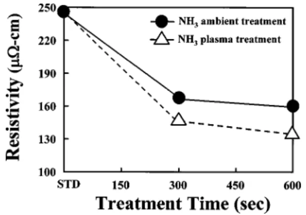
Figure 1 shows the resistivity of these multilayered samples as a function of the time of two different posttreat-ments. The resistivity of these samples decreased with the time of NH3 postannealing and NH3 plasma posttreatment.
The resistivity of these films was reduced from 240 mV cm to 130mV cm after NH3plasma treatment for 600 s. In situ
NH3 plasma posttreatment was found to be effective in
re-ducing the resistivity of TiN films.9 For the investigation of mutilayered CVD-Ti/TiN films, PECVD Ti and multilayered CVD-Ti/TiN were also deposited on the Si substrate in se-quence. The substrate temperature during Ti and TiN film
FIG. 1. Resistivity as a function of the posttreatment time for samples with different treatment methods. Thickness of the samples is 46 nm.
2390 Huet al.: Investigation on multilayered CVD Ti/TiN films 2390
growth was also maintained at 630 °C. A 9.5-nm-thick TiSi2
thin film was formed during the deposition of PECVD Ti on Si. Then a 46-nm-thick mutilayered CVD-Ti/TiN thin film was deposited on TiSi2/Si. Both in situ NH3 postannealing
and in situ NH3plasma posttreatment for 300 s were carried
out to reduce Cl and compensate N concentration in the mul-tilayered CVD-Ti/TiN films. Figure 2 shows the resistivity of these samples as a function of the number of layers. The resistivity of these samples was decreased with the number of Ti/TiN layers. The resistivity of these multilayered CVD-Ti/TiN films can be reduced from 240mV cm ~STD! to 120
mV cm ~III! with NH3plasma treatment for 300 s. Therefore,
increasing the number of multilayered CVDTi/TiN films and the utilization of the plasma post-treatment technique con-tributed to the reduction in the resistivity of TiN films.
The interfaces of TiN/TiSi2/Si structure treated by NH3
plasma for 600 s are seen to be rather smooth in cross-sectional transmission electron microscopy~XTEM! images. The average grain size of TiN film was measured to be about 20 nm. For multilayered CVD-Ti/TiN films, a XTEM image of TiN/Ti/TiN/Ti/TiN/Ti/TiN/TiSi2/Si sample ~sample III!
treated by an in situ NH3 plasma post-treatment for 300 s
shows that the interfaces of Ti/TiN/TiSi2/Si are also rather smooth. An example is shown in Fig. 3. However, the inter-faces of multilayered Ti/TiN in TiN films are not distinct in the XTEM images. It is believed that Ti atoms are distributed fairly uniformly by fast diffusion in TiN films. The average grain size of multilayered CVD-Ti/TiN film was about 20 nm. A plan view micrograph is shown in Fig. 4.
From the AES depth profile, the concentration of Cl in the CVD-TiN/TiSi2/Si sample after NH3 ambient posttreatment
for 30 s was found to be about 3 at. %. Therefore, the STD sample had a high value of resistivity (;240mV cm! which is attributed to the presence of a high density of Ti-Cl bonds in the TiN films. Figure 5 shows the AES depth profile of TiN/Ti/TiN/Ti/TiN/Ti/TiN/TiSi2/Si sample after NH3plasma
posttreatment for 300 s. The concentration of Cl in the sample was found to be about 1.6 at. %, which was lower than that of the STD sample. A previous study showed that chlorine content in excess of 5 at. % would degrade metal reliability and increase the resistivity of the TiN film.9 There-fore, the reduction in Cl content would minimize corrosion of the subsequently deposited Al film. The distribution of Ti1N was found to be fairly uniform in the TiN/Ti/TiN/Ti/ TiN/Ti/TiN/TiSi2/Si samples by AES measurement.
FIG. 3. XTEM image of a multilayered TiN/Ti/TiN/Ti/TiN/Ti/TiN/TiSi2/Si sample treated by in situ NH3plasma posttreatment for 300 s. The rf power of NH3plasma was 500 W. Thickness of the multilayered Ti/TiN sample is 46 nm.
FIG. 4. Plan view image of a multilayered TiN/Ti/TiN/Ti/TiN/Ti/TiN/ TiSi2/Si sample treated by in situ NH3plasma post treatment for 300 s. The rf power of NH3 plasma was 500 W. The thickness of the multilayered Ti/TiN sample is 46 nm.
FIG. 2. Resistivity of various samples with different treatment. Samples were treated by in situ NH3ambient or NH3plasma posttreatment for 300 s. Samples are designated as follows: TiN/TiSi2/Si, as a standard treated by in situ NH3ambient posttreatment for 30 s: STD; TiN/Ti/TiN/TiSi2/Si: ~I!, TiN/Ti/TiN/Ti/TiN/TiSi2/Si: ~II! and TiN/Ti/TiN/Ti/TiN/Ti/TiN/TiSi2/Si: ~III!.
FIG. 5. AES depth profile of a multilayered TiN/Ti/TiN/Ti/TiN/Ti/TiN/ TiSi2/Si sample treated by in situ NH3plasma post treatment for 300 s.
To investigate the distribution of Ti atoms in the multi-layered Ti/TiN films, the 47Ti1N and 51Ti depth profiles were measured by SIMS for the as-deposited multilayered TiN/Ti/TiN/Ti/TiN/Ti/TiN/TiSi2/Si samples. An example is
shown in Fig. 6. It can be seen that the distribution of Ti atoms is fairly uniform in the multilayered Ti/TiN sample. Owing to the TiCl4 etching characteristics, deposition and
etching behavior can occur simultaneously for PECVD Ti deposited on TiN films. As a result, the thickness of PECVD Ti deposited on TiN for 20 s to form multilayered Ti/TiN films is relatively thin. The very thin layer of PECVD Ti deposited on TiN may also fill the grain boundaries of TiN film to improve resistivity.
For Cu electroplating, a 50-nm-thick sputtered Al film was used as a seed layer on the multilayered Ti/TiN films. However, the seed layer cannot be electroplated directly in this study because it will be dissolved in acidic copper elec-troplating solution. Therefore, the seed layer had to be acti-vated by a Pd solution before proceeding to copper electroplating.11The values of applied electrical current were 40-100 mA. A small~002! peak and strong ~111! peak of Cu film are clearly seen in XRD pattern when applied electrical currents were 50, 80 and 100 mA. Examples are shown in Fig. 7. Stronger Cu~111! peak was observed by using higher electrical current. On the other hand, increasing deposition time also leads to stronger Cu~111! when applied electrical
current was fixed, as shown in Fig. 8. The evolution of crys-tal growth orientation of the copper electroplating can be explained by considering surface energy and strain energy of different crystal planes. It is believed that the deposition rate of copper electroplating can be accelerated in the initial stage because the surface of the seed layer is activated by Pd. Therefore, the Cu~002! plane was found to be present owing to the possession of the lowest surface among all crystal planes. As the film thickness and applied electrical current were increased, the strain energy became dominant during grain growth. As a result, stronger Cu~111! was found to be present in samples as the thickness and applied electrical current increased. The electromigration resistance of copper lines was previously reported to be strongly influenced by the copper texture similar to Al lines.12 Stronger Cu ~111! can improve electromigration resistance effectively. Figure 9 reveals the AES depth profile of electroplated Cu/seed layer/ multilayered Ti/TiN sample. The concentration of O in the sample was found to be rather low. Therefore, oxidation of Cu or the seed layer in the samples can be minimized. The seed layer was not dissolved in Cu electroplating solution. However, the surface of as-deposited copper film appeared to be rather rough which resulted in the increase in resistivity to 2.34 mV cm. Bright and smooth copper film surface can be achieved by chemical mechanical polishing ~CMP! technol-ogy.
FIG. 6. SIMS depth profile of a multilayered TiN/Ti/TiN/Ti/TiN/Ti/TiN/ TiSi2/Si sample treated by in situ NH3plasma post treatment for 300 s.
FIG. 7. XRD peaks of electroplated Cu films for which the applied electrical currents are 50, 80 and 100 mA and the deposition time is 3 min.
FIG. 8. XRD peaks of electroplated Cu films for which the deposition times are 1 and 5 min and applied electrical current is 80 mA.
FIG. 9. AES depth profile of an electroplated Cu/seed layer/multilayered Ti/TiN sample. The thickness of the seed layer is 50 nm.
2392 Huet al.: Investigation on multilayered CVD Ti/TiN films 2392
The p-n junctions are basic building blocks of current semiconductor technology, and when they fail to perform properly, production yields suffer. The leakage current of
n1- p junctions is the most sensitive and also the most rel-evant test to ascertain the effectiveness of the diffusion bar-rier. The diffusion of Al and Si through the barrier would gradually cause the decrease of junction depth. Figure 10 shows the leakage currents of the Al/TiN/TiSi2/n1Si~STD!,
Al/TiN/Ti/TiN/TiSi2/n1Si~sample I! and Al/TiN/Ti/TiN/Ti/
TiN/TiSi2/n1Si ~sample II! contact systems that were
an-nealed at 400–600 °C for 30 min in N2 ambient. From Fig.
10, after annealing at 575 °C for 30 min, contact systems using TiN/TiSi2as barrier layer exhibited large leakage
cur-rent which indicated that the diffusion of Al and Si through the barrier occurred. The grains of the TiN films were of columnar structure which facilitates fast diffusion. Figure 11 shows that the leakage current is significantly improved by the multilayered Ti/TiN film with NH3plasma posttreatment after annealing at 585 °C for 30 min compared with a PVD-TiN barrier. As a result, the multilayered CVD-Ti/PVD-TiN struc-ture is effective in enhancing the barrier property because the
very thin layer of PECVD Ti deposited on TiN may stuff the grain boundaries of the TiN film and thus retard Al/Si inter-diffusion.
IV. CONCLUSIONS
The resistivity of the multilayered CVD-Ti/TiN films can be reduced from 240 mV cm ~standard sample! to 120
mV cm with NH3plasma posttreatment for 300 s. Increasing
the number of Ti/TiN layers in the multilayered CVD-Ti/TiN films and use of the plasma posttreatment technique contrib-uted to the reduction in the resistivity of the TiN films. Smooth multilayered Ti/TiN films were observed in XTEM images. The content of chlorine in the multilayered CVD-Ti/ TiN film was 1.6 at. %. The low Cl content can minimize corrosion in subsequent metal film ~Al or Cu!. SIMS depth profiles of the multilayered Ti/TiN sample showed that Ti atom distribution is fairly uniform. Cu film was electroplated on the multilayered CVD-Ti/TiN films. A small ~002! peak and strong ~111! peak of Cu were seen in the XRD pattern. The evolution of crystal growth orientation of the copper electroplating can be explained by considering surface en-ergy and strain enen-ergy of different crystal planes. The leak-age current is significantly improved by the multilayered CVD-Ti/TiN film with NH3 plasma posttreatment after
an-nealing at 585 °C for 30 min compared with a PVD-TiN barrier. Multilayered CVDTi/TiN structure is effective in en-hancing the barrier property since the very thin layer of PECVD Ti deposited on TiN may stuff the grain boundaries of the TiN film to retard metal/Si interdiffusion.
ACKNOWLEDGMENTS
The work was supported by the National Nano Device Laboratory and National Science Council of the Republic of China under Contract Nos. NSC88-2215-E317-009 and NSC87-27212317-200.
1
R. I. Hedge, R. W. Fiordalice, E. O. Travis, and R. J. Tobin, J. Vac. Sci. Technol. B 11, 1287~1993!.
2J. S. Byun, C. R. Kim, K. G. Rha, and J. J. Kim, Jpn. J. Appl. Phys., Part 1 34, 978~1995!.
3C. Faltermeter, C. Goldberg, M. Jones, A. Upham, D. Manger, G. Peter-son, J. Lau, A. E. Laloyeros, B. Arkles, and A. Paranjpe, J. Electrochem. Soc. 144, 1002~1997!.
4J. T. Hillman, Proceedings of the 1995 SEMI Taiwan Technical Confer-ence,~SEMI Taiwan, Taipei, Taiwan, 1995!, p. 8.
5
J. Faguet, C. Arena, E. Guidotti, R. F. Foster, and J. T. Hillman, Ad-vanced Metallization for ULSI Applications in 1995~MRS, Pittsburgh, 1995!, p. 259.
6T. Suzuki, T. Ohba, Y. Furumura, and H. Tsutikawa: Proceedings of the 10th International VLSI Multilevel Interconnection Conference ~IEEE, New York, 1993!, p. 418.
7Y. J. Mei, T. C. Chang, J. C. Hu, L. J. Chen, Y. L. Yang, F. M. Pan, W. F. Wu, A. Ting, and C. Y. Chang, Thin Solid Films 308, 594~1997!. 8J. C. Hu, T. C. Chang, L. J. Chen, Y. L. Yang, and C. Y. Chang, Thin
Solid Films 332, 423~1998!. 9
P. Singer, Semicond. Int. 21, 91~1998!. 10P. Singer, Semicond. Int. 20, 67~1997!.
11C. H. Ting and M. Paunovic, J. Electrochem. Soc. 136, 456~1989!. 12T. Kaizuka, H. Shinriki, N. Takeyasu, and T. Ohta, Jpn. J. Appl. Phys.,
Part 1 33, 470~1994!. FIG. 10. Leakage currents of contact systems in various samples annealed at
400–600 °C for 30 min in N2ambient.
FIG. 11. Leakage currents of contact systems in various samples annealed at 585 °C for 30 min in N2ambient.