Effects of Channel Width and NH
3Plasma Passivation on
Electrical Characteristics of Polysilicon Thin-Film Transistors
by Pattern-Dependent Metal-Induced Lateral Crystallization
Yung-Chun Wu,aTing-Chang Chang,b,d,*
,zCheng-Wei Chou,a Yuan-Chun Wu,a Po-Tsun Liu,cChun-Hao Tu,aWen-Jun Huang,dJen-Chung Lou,aand
Chun-Yen Changa a
Institute of Electronics, National Chiao Tung University, Taiwan b
Department of Physics and Institute of Electro-Optical Engineering, National Sun Yat-Sen University, Taiwan
c
Department of Photonics and Display Institute, National Chiao Tung University, Taiwan d
National Nano Device Laboratory, Taiwan
This work studied the effects of channel width and NH3 plasma passivation on the electrical characteristics of a series of pattern-dependent metal-induced lateral crystallization共PDMILC兲 polysilicon thin-film transistors 共poly-Si TFTs兲. The perfor-mance of PDMILC TFTs improves as each channel width decreasing. Further, PDMILC TFTs with NH3plasma passivation outperforms without such passivation, resulting from the effective hydrogen passivation of the grain-boundary dangling bonds, and the pile-up of nitrogen at the SiO2/poly-Si interface. In particular, the electrical characteristics of a nanoscale TFT with ten 67 nm wide split channels共M10兲 are superior to those of other TFTs. The former includes a higher field effect mobility of 84.63 cm2/V s, a higher ON/OFF current ratio共⬎106兲, a steeper subthreshold slope 共SS兲 of 230 mV/decade, and an absence of drain-induced barrier lowering共DIBL兲. These findings originate from the fact that the active channels of the M10 TFT have exhibit the most poly-Si grain enhanced to reduce the grain boundary defects and the best NH3plasma passivation. Both effects can reduce the number of defects at grain boundaries of poly-Si in active regions for high performances.
© 2005 The Electrochemical Society. 关DOI: 10.1149/1.1931473兴 All rights reserved.
Manuscript submitted November 5, 2004; revised manuscript received February 7, 2005. Available electronically June 7, 2005.
The major attraction of applying polycrystalline silicon thin-film transistors 共poly-Si TFTs兲 in active matrix liquid crystal display
共AMLCDs兲 lies in the greatly improved carrier mobility 共larger than
10 cm2/V s兲 in poly-Si film and the capability of integrating the pixel switching elements, the panel array, and the peripheral driving circuit on the same substrate,1-3 bring the era of system-on-panel
共SOP兲 technology. For making high performance poly-Si thin film
transistors 共TFTs兲, low-temperature technology is required for the realization of commercial flat-panel displays on inexpensive glass substrates, which the maximum process temperature is limited to less than 600°C. There are three major low-temperature amorphous-Si crystallization methods to achieve high performance poly-Si thin film: solid phase crystallization共SPC兲,4excimer laser crystallization 共ELC兲,5 and metal-induced lateral crystallization
共MILC兲.6-10
MILC technology was initially developed as a temperature crystallization technique compared to other low-temperature poly-Si technologies such as ELC or conventional SPC. MILC is superior because, unlike ELC, it is a low-cost batch process and, unlike SPC, a better quality poly-Si thin film can be obtained. In addition, the presence of poly-Si grain boundary defects in the channel region of TFTs drastically affects the electrical characteris-tics, especially when the device dimension is scaled down. There-fore, reducing the number of polysilicon grain boundary defects will improve the performance of poly-Si TFTs. The poly-Si TFTs with several multichannels have been reported to effectively reduce grain boundary defects.11,12Thus, we demonstrate a practicable method to reduce the poly-Si grain boundary defects by using a structure modulation MILC process共i.e., PDMILC兲 to fabricate the high per-formance TFTs. Moreover, NH3plasma passivation13has been re-ported to reduce the number of trap states in poly-Si grain bound-aries, yielding high-performance poly-Si TFTs. Therefore, in this work the effects of channel width and NH3plasma passivation on the electrical characteristics of a series of multichannels with differ-ent widths PDMILC poly-Si TFTs were investigated.
Device Structure and Fabrication
In this work a series of PDMILC TFTs, with a gate length of 5m, consisting of ten strips of multiple 67 nm wire channels
共M10兲 TFT, five strips of multiple 0.18 m channels 共M5兲 TFT, two
strips of 0.5m channels 共M2兲 TFT, and a single-channel structure
共S1兲 with width of 1 m TFT, were fabricated, as listed in Table I.
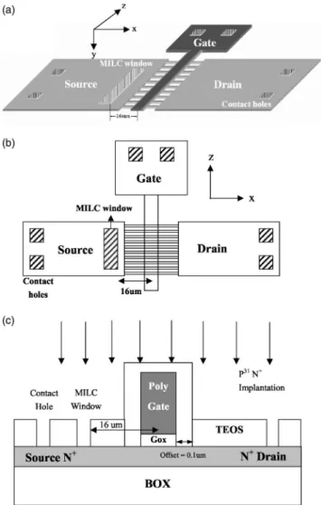
Figure 1a shows a schematic plot and Fig. 1b shows a top view of PDMILC TFT with source, drain, gate, nanowires channels and MILC seeding window. Figure 1c shows the cross-section view of PDM-TFT, which was a conventional top-gate, offset metal-oxide-semiconductor field-effect transistor共MOSFET兲 structure.
The 6 in. p-type single crystal silicon wafers were coated with 400 nm thick SiO2as the starting materials. Undoped 50 nm thick amorphous-Si共a-Si兲 layer were deposited by low-pressure chemical vapor deposition 共LPCVD兲 at 550°C. Then the active islands, in-cluding source, drain, and ten nanowire channels were patterned by electron beam lithography 共EBL兲 and transferred by reactive ion etching共RIE兲. After defining the active region, the 25 nm thick tet-raethylorthosilicate共TEOS兲 SiO2was deposited by LPCVD as gate insulator. Then, 150 nm thick undoped poly-Si films were deposited immediately on the gate oxide by LPCVD. The poly-Si layers were patterned by EBL and transferred by RIE to define the gate elec-trode. After gate formation, a 100 nm thick TEOS-SiO2layer used as a passivation layer was deposited by LPCVD. The poly-Si gate sidewall TEOS-SiO2 formed a self-aligned offset spacer with a width of 0.1m, as shown in Fig. 1c. Then, the MILC seeding window and contact holes were patterned by EBL and transferred by RIE in the same mask process. Then, a thin 10 nm thick nickel共Ni兲 layer was deposited by physical vapor deposition共PVD兲. The MILC crystallization was carried out at 550°C for 48 h in an N2ambient. The average lateral crystallization length was about 30m, as shown in Fig. 2b共inset兲. After annealing for a long time, the unre-acted nickel on passivative TEOS-SiO2were removed by a H2SO4 solution at 120°C within 10 min. Phosphorus ions at a dose of 5
⫻ 1015cm−2were implanted through the passivative TEOS-SiO 2to form the n+ gate, the source/drain regions and the self-aligned offset region were formed in the same process step, as shown in Fig. 1c. Next, the dopants were activated by rapid thermal annealing at 850°C with 30 s. The 300 nm thick aluminum共Al兲 layer was de-*Electrochemical Society Active Member.
posited by PVD and patterned for source, drain, and gate metal pads. Then, the finished devices were sintered at 400°C for 30 min in an N2ambient. Finally, each device was passivated by a NH3plasma treatment for 2 h at 300°C.
Results and Discussion
Figure 2a presents an after etching investigation scanning elec-tron microscope共SEM兲 photograph of the poly-Si active region of the M10 TFT, including the source, the drain, ten multiple nanowire
channels, and the MILC seeding window. The inset plot of Fig. 2a presents a magnified area of the multiple nanowire channels in the M10 TFT, each of which is 67 nm wide. Figure 2b presents a SEM photograph of the MILC poly-Si grains in the active region of the proposed TFTs. The average grain size in the poly-Si channel formed by MILC is approximately 250 nm. The inset optical mi-croscopy photography depicts a MILC length of 30m, which is longer than 16m 共Fig. 1a兲, to ensure that the whole active channel was crystallized by the MILC process.
Figure 3a-d shows that the S1, M2, M5, and M10 PDMILC TFTs transfer characteristics with and without NH3 plasma passivation. These results reveal that device performance was enhanced with a decrease in each channel width. Meanwhile, the device that had undergone NH3plasma passivation outperforms that without NH3 plasma passivation. The former has a higher field effect mobility
共FE兲, a higher ON/OFF ratio, a lower threshold voltage 共Vth兲, a lower subthreshold slope 共SS兲, and a lower drain-induced barrier lowering共DIBL兲. The device parameters vs. multichannels with dif-ferent widths are plotted to elucidate the effect of NH3plasma pas-sivation on each of the dimensions of PDMILC TFTs.
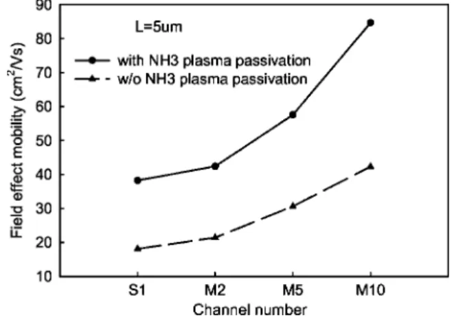
Figure 4 plots theFE of the PDMILC TFTs vs. the multichan-nels with different widths, with and without NH3plasma passiva-tion. TheFE is extracted from the linear region共Vd= 0.1 V兲 of transconductance共gm兲. This curve reveals that FEof PDMILC TFT was enhanced with a decrease of each channel width.共or the number of channels increases兲. The results suggest that during the MILC process, the poly-Si grain lateral length increases as the channel
Table I. Devices dimension of S1, M2, M5, and M10 PDMILC poly-Si TFTs. All devices have the same active channel thickness of 50 nm and gate TEOS-oxide thickness of 25 nm.
Device name Gate length, L 共m兲 Channelnumber Each channel width, W 共m兲 Effective channel width, Weff 共m兲 S1 5 1 1 1 M2 5 2 0.5 1 M5 5 5 0.18 0.9 M10 5 10 0.067 0.67
Figure 1. 共a兲 Schematic plot of PDMILC poly-Si TFT with source, drain,
gate, ten nanowires channels, contact holes and MILC seeding window.共b兲 Top view of PDMILC poly-Si TFT. The key process flows are active region pattering, gate patterning, MILC seeding window and contact holes pattern-ing, and all metal pads pattering. 共c兲 Cross-sectional view of PDMILC poly-Si TFT, which was a conventional MOSFET with offset structure.
Figure 2.共a兲 SEM photography of active pattern with the source, the drain,
ten nanowire channels and MILC seeding window. The inset plot shows the each nanowire width of 67 nm.共b兲 SEM photography of MILC poly-Si grain structure. The average poly-Si lateral grain size is about 250 nm. The inset optical microscopy photography depicts a MILC length of 30m.
width declines. Therefore, the grain boundary defects of ploy-Si will be reduced to increase the mobility. Moreover, NH3plasma passi-vation further improves theFEof a PDMILC TFT, suggesting that the NH3plasma effectively hydrogen passivated the dangling bonds at the grain boundary and the pile up of nitrogen at the SiO2 /poly-Si interface. In particular, the M10 PDMILC TFT has the most improved FE at 84.63 cm2/V s, because it has a split nanowire structure, which can greatly enhance poly-Si gain during the MILC process, and is exposed most effectively to an atmosphere of NH3 plasma. Figure 5 plots the Vthof the PDMILC TFTs vs. the multi-channel with different widths. The Vthis defined by constant current extraction, as the gate voltage required to yield normalized drain current of Id/共W/L兲 = 10−7A at Vd= 5 V. After NH3plasma passi-vation, the Vthof each TFT device was approximately 4 V lower. Because of NH3plasma passivation reduced the barrier height共EB兲 of the poly-Si grain boundary, the electrons can easily overcome EB, producing a high current and allowing the TFT to be easily turned on. Also, the pileup of nitrogen at the SiO2/poly-Si interface will
Figure 3. Device transfer characteristics Id-Vg curve of 共a兲 S1 共W/L = 1 m/5 m兲, 共b兲 M2 共W/L = 0.5 m ⫻ 2/5 m兲, 共c兲 M5 共W/L = 0.18 m ⫻ 5/5 m兲, and 共d兲 M10 共W/L = 67 nm ⫻ 10/5 m兲 PDMILC poly-Si TFT, with 共solid line兲 and without 共dash-line兲 NH3plasma passivation.
Figure 4. FEof PDMILC poly-Si TFTs vs. multichannels with different widths, with and without NH3plasma passivation.
reduce the interface trap density. Such a low value of Vthof the PDMILC TFT is appropriate in low-power AMLCD applications. Figure 6 plots the subthreshold swing共SS兲 of the PDMILC TFTs vs. the multichannels with different widths, with and without NH3 plasma passivation. The parameter SS is directly related to the total trap states density共NT兲 by14
SS =
冉
kTq
冊
ln 10冉
1 + q2tSiNTCox
冊
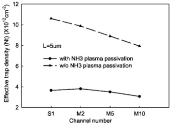
where kT is thermal energy, Coxis the gate oxide capacitance per unit area, and tSiis the poly-Si layer thickness. Before NH3plasma passivation, the results reveal the decline of SS as each channel width decreases from S1, M2, and M5 to M10 TFT, and suggests that increasing the lateral size of the poly-Si grain reduces NT. Moreover, NH3plasma passivation further reduces SS, because of the pileup of nitrogen at the SiO2/poly-Si interface and the hydrogen passivation of the dangling bonds at the grain boundary. The amount of effects of NH3 plasma passivation on PDMILC TFTs poly-Si grain boundaries can be evaluated from the grain boundary defects density共Nt兲.15Figure 7 plots extraction curves of Ntof M10 PD-MILC TFTs, with and without NH3 plasma passivation. Figure 8 plots Nt of PDMILC TFT vs. the multichannels with different widths, with and without NH3plasma passivation. The Ntdecreases gradually from S1, M2, and M5 to the M10 PDMILC TFT with each
channel width of the TFTs decreasing. Moreover, NH3plasma pas-sivation substantially reduces Nt, providing high electrical perfor-mance. In addition, the M10 TFT has the lowest Nt 共3.07
⫻ 1012cm−2兲 and this value is consistent with its best performance. Conclusion
Experimental results indicate that the performance of devices improves as each channel width decreases from the S1, M2, and M5 to the M10 PDMILC TFT. Moreover, the performance of devices further improves with NH3plasma passivation. The defect density
共Nt兲 in the grain boundary reveals a strong consistency between theory and experimental results. Notably, M10 TFT has the best electrical performance. Because the M10 TFT has a split nanowire structure, which can greatly enhance poly-Si gain during the MILC process, and is exposed most effectively to an atmosphere of NH3 plasma than other dimension TFTs. Both effects can reduce the number of defects at poly-Si grain boundaries in the active channel. In summary, we successfully demonstrate a practicable method to fabricate the high performance TFTs by structure modulation MILC process共PDMILC兲. Meanwhile, using NH3plasma passivation, the PDMILC TFTs can further improve the performance. These high performance NH3plasma passivation PDMILC TFTs are compatible with complementary metal-oxide-semiconductor technology, thus highly suitable for use in future SOP applications.
Figure 5. Vth of PDMILC poly-Si TFTs vs. multichannels with different widths, with and without NH3plasma passivation.
Figure 6. SS of PDMILC poly-Si TFTs vs. multichannels with different
widths, with and without NH3plasma passivation.
Figure 7. Extraction of Ntplot of the M10 PDMILC TFTs, with and without NH3plasma passivation.
Figure 8. Nt of PDMILC poly-Si TFTs vs. multichannels with different widths, with and without NH3plasma passivation.
Acknowledgments
The authors would like to acknowledge the National Science Council of the Republic of China, Taiwan for financially supporting this research under contract no. NSC 93-2112-M-110-008. The Na-tional Nano Device Laboratory is appreciated for its technical support.
National Sun Yat-Sen University assisted in meeting the publication costs of this article.
References
1. K. Nakazawa, J. Appl. Phys., 69, 1703共1991兲.
2. T. J. King and K. C. Saraswat, IEEE Electron Device Lett., 13, 309共1992兲. 3. H. Kuriyama, S. Kiyama, S. Noguchi, T. Kuahara, S. Ishida, T. Nohda, K. Sano,
H. Iwata, S. Tsuda, and S. Nakano, Tech. Dig. - Int. Electron Devices Meet., 1991, 563.
4. N. Yamauchi and R. Reif, J. Appl. Phys., 75, 3235共1994兲. 5. H. J. Kim and J. S. Im, Appl. Phys. Lett., 68, 1513共1996兲. 6. S. W. Lee and S. K. Joo, IEEE Electron Device Lett., 17, 160共1996兲. 7. H. Wang, M. Chan, S. Jagar, V. M. C. Poon, M. Qin, Y. Wang, and P. K. Ko, IEEE
Trans. Electron Devices, 47, 1580共2000兲.
8. Z. Meng, M. Wang, and M. Wong, IEEE Trans. Electron Devices, 47, 404共2000兲. 9. V. W. C. Chan and P. C. H. Chan, IEEE Electron Device Lett., 22, 80共2001兲. 10. A. R. Joshi and K. C. Saraswat, J. Electrochem. Soc., 150, G443共2003兲. 11. T. Unagami and O. Kogure, IEEE Trans. Electron Devices, 35, 1986共1988兲. 12. Y. C. Wu, T. C. Chang, C. Y. Chang, C. S. Chen, C. H. Tu, P. T. Liu, H. W. Zan,
and Y. H. Tai, Appl. Phys. Lett., 84, 3822共2004兲.
13. H. C. Cheng, F. S. Wang, and C. Y. Huang, IEEE Trans. Electron Devices, 44, 64
共1997兲.
14. C. A. Dimitriadis, J. Appl. Phys., 88, 3624共2000兲.
15. R. E. Proano, R. S. Misage, and D. G. Ast, IEEE Trans. Electron Devices, 36, 1915共1989兲.