654 IEEE ELECTRON DEVICE LElTERS, VOL. 13, NO. 12, DECEMBER 1992
Gate and Drain Currents in Off-State
Buried-Type p-Channel
LDD MOSFET’s
Ming-Jer Chen,
Member, IEEE,Kum-Chang Chao, Tzuen-Hsi Huang, and Jyh-Min Tsaur
Abstract-The buried-type p-channel LDD MOSFET’s biased at high positive gate voltage exhibit new characteristics: 1) the ratio of the drain to gate currents is about 1 X to 5 X 10 -3; and 2) the gate and drain currents both are functions of
only the gate voltage minus the n-well bias. Such characteristics are addressed based on the formation of the surface n + inver- sion layer due to the punchthrough of the buried channel to the underlying shallow p-n junction. The measured gate current is due to the Fowler-Nordheim tunneling of electrons from this inversion layer surface and the holes generated within the high-field oxide constitute the drain current. The n + inversion
layer surface potential is found to be equal to the n-well bias plus 0.55 V. As a result, not only the oxide field but also the gate and drain currents are independent of drain voltage.
I. INTRODUCTION
ECENTLY, the off-state MOSFET’s or equivalently
R
the gate-controlled reverse-bias diodes have been extensively investigated and the associated phenomena have been newly reported [11-[71. In the work of [11-[71, the gate current is reported to be less than the drain current by several orders of magnitude and/or both are strong functions of drain voltage. Based on the off-state buried-type p-channel LDD-MOSFET’s, however, we have found that not only is the drain current less than the gate current by several orders of magnitude, but also both are independent of drain voltage. In this letter, we will report such new I-V characteristics and the corresponding inter- pretations.Manuscript received July 31, 1992; revised October 12, 1992. This work was supported by the National Science Council under Contract M.-J. Chen, K.-C. Chao, and T.-H. Huang are with the Institute of Electronics, National Chiao-Tung University, Hsin-Chu, Taiwan, Repub- lic of China.
J.-M. Tsaur is with Taiwan Semiconductor Manufacturing Company, Hsin-Chu, Taiwan, Republic of China.
IEEE Log Number 9205343. NSC 81-0404-E-OO9-113.
11. EXPERIMENT
The devices were fabricated by a 0.8-pm twin-well polycide CMOS process. The starting material was p-type (100)-oriented Si wafers with resistivity of 10 R
.
cm. Phosphorus (6.5 X 10l2 cmp2, 80 keV) was implanted to form the n-well region. BF, (2.8 Xlo’,
cm-,, 80 keV) was used as the threshold voltage implant. The gate oxide was grown in dry 0, at 920°C to a thickness of 180A.
After gate poly deposition and phosphorus doping, a layer of WSi, (2500A)
was deposited and annealed at 920°C to form the n + polycide gate. BF, (lOI3 cm-,, 50 keV) was implanted to form the low-doped drain region. After the sidewall spacer (3000A)
was formed, BF, ( 3 X l O I 5 cmp,,
80 keV) was implanted to form the highly doped drain region.With the source floating and the n-well grounded, each structure with the assigned drain terminal condition has been characterized by measuring the gate and drain cur- rents as function of gate voltage ranging from 16 to 21 V. Fig. 1 shows the corresponding measurement results for three drain voltages, 0, -3, -5 V, and also with the drain floating. From Fig. 1 it can be clearly observed that 1) the drain current is less than the gate current with an ID/IG
ratio of about 1 X to 5 X l o p 3 ; 2) both the gate and drain currents are independent of drain voltage; and 3) the gate current is not affected when the drain is floated. Moreover, the characterization has been performed for n-well bias V,, = 0 and 2 V under VD = -3 V and the
corresponding results are shown in Fig. 2. From Fig. 2 we can observe that as the n-well bias changes from 0 to 2 V, not only the gate current versus gate voltage characteris- tics but also the drain current versus gate voltage charac- teristics are shifted right by a value of about 2 V.
111. DISCUSSION
Based on the observations mentioned above, the prob- lem can be simply reduced to the Fowler-Nordheim tun- neling in a single metal-oxide-p-n diode, i.e., as the gate voltage increases positively to deplete the p-channel re- 0741-3106/92$03,00 0 1992 IEEE
~-
_ _ _ _ _ ~ ~ pp
CHEN et al.: GATE AND DRAIN CURRENTS IN BURIED-TYPE P-CHANNEL LDD MOSFET'S 10-4
-
10-54
2
10-68
5
10-7.s
10-82
n
U U 8 10-9 + 10-10 U U2
U5
10-1' al c, 0 io-L2r --
- - - - - - 110-9 V&'ov
-v,
=ov
- - -v,
= -3v . . .v,
= -5v _ . _ . _ . Drain Floating-
Eq.(l) for IG - 10-2 - 10-9 1 I I l U - ' r n - i 3 lo-*: 14 16 I 8 20 22 24" Gate Voltage V, (V)Measured gate and drain currents as function of gate voltage for two n-well biases of 0 and 2 V under the same Fig. 2.
drain voltage of -3 V. Gate width is 100 pm.
656 IEEE ELECTRON DEVICE LETTERS, VOL. 13, NO. 12, DECEMBER 1992
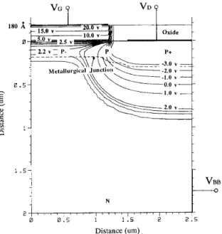
gion under the oxide until the punchthrough to the shal- low p-n junction occurs, the electrons will be injected from the n-well to the surface where an n + inversion layer under the oxide is thus formed. The device simulator PISCES-IIB is used to predict the potential distributions, from which we have concluded that the inversion-layer surface potential is equal to the n-well bias plus 0.55 V and is independent of both gate voltage and drain voltage. Simulation results are shown in Fig. 3 where the potential
contours are plotted for V, = -3 V, V, = 20 V, and
V,, = 2 V. Similar results are obtained with V,, = 0 V. This can be justified by the measurement of changing the n-well bias as shown in Fig. 2.
Therefore, the F-N tunneling of conduction-band elec- trons from the inversion surface dominates the gate cur- rent. To confirm this interpretation, the calculation of the F-N current I, as function of oxide field E,, is per- formed using the following equations 181:
I, = A G . ~ . E , & . e x p ( - p / E , , ) and
where A,( = 150 F m 2 ) is the oxide area, to,( = 180
A)
is the oxide thickness, VF,(=0.44 V as measured by CVmethod) is the flat-band voltage, and q s ( = V,,
+
0.55 V as mentioned above) is the associated surface potential. The values of the preexponential constant CY( = 4.12 Xlo-' A / V 2 ) and the physical constant p(=2.42 X lo8 V/cm) have been obtained by fitting the low-level range of gate current in Fig. 1. These fitting values are close to those of a = 2.3 x A / V 2 and
p
= 2.385 X l o 8 V/cm as cited in [8]. The deviation at the high V, values in Fig. 1 may be due to the enhancement of the local field in the oxide which is caused by the trapped holes 191.One may propose several mechanisms such as band-to- band tunneling [ 11, [2], silicon valence-band electron tun- neling [ lo], and hole generation within the high-field oxide [ l l ] , [12] to account for the observed drain currents. However, the band-to-band tunneling mechanism is not accepted here since it is a strong function of drain voltage [1]-[7]. The ratio of the silicon valence-band electron tunneling to the conduction-band electron tunneling has been estimated to be about [ll], [12]. Thus, the silicon valence-band electron tunneling mechanism can- not account for our measured ratio of 1 x
lo-'
to 5 Xlo-'. According to the work of 1111, not only the holes generated inside the high-field oxide are linked to the conduction-band electron tunneling from the n + inversion layer surface, but also both are function of only the oxide field. Therefore, the collection of the holes generated within the high-field oxide is suggested to be the origin of our measured drain currents.
Note that for the n-channel MOSFET's connected as
180 A
0
l 0 . 5 . Distance 1 . 5 (urn) 1 2 . 5 1
Fig. 3. Simulated potential contours corresponding to V, = -3 V, VG = 20 V, and V,,
7
2 V. The parameter of flat-band voltage V,, = 0 V was used in simulation.the gate-controlled nt-p diodes with the n + inversion layer induced under the oxide, the gate and substrate hole currents have been shown to be due to the silicon conduc- tion-band electron tunneling and the collection of the holes generated inside the oxide, respectively [ 111, [12]. Fig. 4 shows the corresponding gate and hole collection current densities versus oxide field for two oxide thick- nesses of 154 and 200
A
(see [ll, fig. 11). In Fig. 4 we also present the results obtained from Fig. 1 where the drain current represents the hole collection current. Based on Fig. 4, it can be concluded that our I-I/ characteristics measured from the off-state buried-type p-channel LDD MOSFET's are analogous to those from the gate-con- trolled n+-p diodes having the n + inversion layer. The relationships between the two are: 1) the drain hole current in our work corresponds to the substrate hole current in [ll] and [12]; 2) the electrons within the surface n + inversion layer are provided by the injection from the n-well in our work while in [ l l ] and [12] the n + inversion layer beneath the gate oxide is electrically connected to the n' drain region.IV. CONCLUSION
The drain and gate currents measured from the off-state buried-type PMOSFET's have been found to be indepen- dent of drain voltage. The electron F-N tunneling from the n + inversion layer surface and the collection of the holes generated inside the oxide can be applied to reason- ably explain our measured results. The analogies between the off-state buried-type p-channel LDD MOSFET's and
CHEN et al.: GATE AND DRAIN CURRENTS IN BURIED-TYPE P-CHANNEL LDD MOSFET’S 65 7 : Chen, et al.‘s Data [11]
: This work I 10-1 - m -E
2
10-2 - W x . a .- gB
-
: Chen, et al.‘s Data [11] 100 - : This work 10-1 - m -E2
10-2 - W x . a .- gB
g
d
-
-= 10-4-f
-
l o * - I O * - 10-7-
- 10-7 B 10 12 14 - l o * I O * ‘ ’Oxide Field Strength E,, (MV/cm)
-
-= 10-4-g
d
f
-
l o * - I O * -10--
10-7 - 10-7 -z
-
/ B 10 12 14 - l o * I O * ‘ ’Oxide Field Strength E,, (MV/cm)
I U
110-4
.!
I O *
=
Fig. 4. Comparisons of the measured gate and hole collection current densities versus oxide field as cited in [11] and those corresponding to Fig. 1 . Here the drain current in Fig. 1 represents the hole collection current and the substrate hole current in 1111 represents the hole collection current.
the gate-controlled n+-p diodes with the n + inversion 161 J. Chen, T. Y. Chan, P. K. KO, and C. Hu, “Gate current in off-state MOSFET,” IEEE Electron Decice Lett., vol. 10, pp. 203-205, 1989.
layer have also been addressed.
[41
REFERENCES
C. Chang and J. Lien, “Corner-field induced drain leakage in thin oxide MOSFETs,” in IEDM Tech. Dig., 1987, pp. 714-717. T. Y. Chan, J. Chen, P. K. KO, and C. Hu, “The impact of gate-induced drain leakage current on MOSFET scaling,” in IEDM Tech. Dig., 1987, pp. 718-721.
I. C. Chen, D. J. Coleman, and C. W. Teng, “Gate current injection initiated by electron band-to-band tunneling in MOS devices,” IEEE Electron Decice Lett., vol. 10, pp. 297-300, 1989. M. J. Chen, “Effect of back-gate bias on tunneling leakage in a gated p+-n diode,” IEEE Electron Delice Lett., vol. 12, pp. 249-251, 1991.
C. Chang, S. Haddad, B. Swaminathan, and J. Lien, “Drain- avalanche and hole-trapping induced gate leakage in thin oxide MOS devices,” IEEE Electron Decice Lett., vol. 9, pp. 588-590, 1988.
[7] M. J. Chen, “New observation of gate current in off-state MOS- FET,” IEEE Trans. Electron Deuices, vol. 38, pp. 2118-2120, 1991. [8] Z . A. Weinberg, “On tunneling in metal-oxide-silicon structures,” [9] I. C. Chen, S. E. Holland, and C. Hu, “Electrical breakdown in thin gate and tunneling oxides,’’ IEEE J. Solid-state Circuits, vol. B. Eitan and A. Kolodny, “Two components of tunneling current in metal-oxide-semiconductor structures,” Appl. Phys. Lett., vol. [ l l ] I. C. Chen, S. Holland, K. K. Young, C. Chang, and C. Hu, “Substrate hole current and oxide breakdown,” Appl. Phys. Lett.,
[12] Z . A. Weinberg and M. C. Fischetti, “Investigation of the SO,-in- duced substrate current in silicon field-effect transistors,” J. Appl.
J. Appl. Phys., vol. 53, pp. 5052-5056, 1982.
SC-20, pp. 333-342, 1985. [lo]
43, pp. 106-108, 1983.
vol. 49, pp. 669-671, 1986.
![Fig. 4. Comparisons of the measured gate and hole collection current densities versus oxide field as cited in [11] and those corresponding to Fig](https://thumb-ap.123doks.com/thumbv2/9libinfo/7632256.135384/4.919.255.641.101.424/comparisons-measured-collection-current-densities-versus-oxide-corresponding.webp)
