Ge Epitaxial Growth on GaAs Substrates for Application
to Ge-Source/Drain GaAs MOSFETs
Guang-Li Luo,a,zZong-You Han,bChao-Hsin Chien,a,bChih-Hsin Ko,c Clement H. Wann,c Hau-Yu Lin,c Yi-Ling Shen,a Cheng-Ting Chung,b Shih-Chiang Huang,aChao-Ching Cheng,band Chun-Yen Changb
a
National Nano Device Laboratories, Hsinchu 300, Taiwan b
Department and Institute of Electronics Engineering, National Chiao-Tung University, Hsinchu 300, Taiwan
c
Taiwan Semiconductor Manufacturing Company, Limited, Hsinchu 300, Taiwan
Ge films were epitaxially grown on GaAs共100兲 substrates and Ga0.88In0.12As共100兲 virtual substrates using an ultrahigh vacuum/
chemical vapor deposition system. The incubation time of Ge growth depends on Ga共In兲As surfaces that were processed by different wet chemical solutions. Growth behaviors, such as island growth at the initial stages and selective growth into recessed regions of GaAs, were studied by transmission electron microscopy. To test the quality of Ge grown on GaAs, an n+-Ge/p-GaAs
diode was fabricated. We propose that through Ge selective epitaxial growth, Ge can be used as the source–drain of a GaAs metal-oxide-semiconductor field-effect transistor共MOSFET兲 to overcome some intrinsic limitations of this device.
© 2009 The Electrochemical Society. 关DOI: 10.1149/1.3246000兴 All rights reserved.
Manuscript submitted July 15, 2009; revised manuscript received September 8, 2009. Published November 3, 2009.
For the past few decades, advances in Si complementary metal oxide semiconductor共CMOS兲 technology have been driven by de-vice scaling, which has increased performance as well as reduced costs and controlled power consumption. However, as devices are scaled below 100 nm, the performance gain attributable to scaling is diminished. Presently, in industry, device performance is improved by mobility enhancement and achieved by applying strain to con-ventional Si metal-oxide-semiconductor field-effect transistors 共MOSFETs兲 either through process-induced strain1
or through sub-strate engineering.2 However, the mobility benefits that can be achieved by straining Si are limited and are reduced by scaling, and there is a great interest in studying non-Si channel materials that have an even higher mobility enhancement potential. Fortunately, III-Vs promise to increase electron mobility by a factor of 10–30 times, which makes them great candidates for high speed, low power n-channel transistors.3 However, III-Vs cannot make good p-channels, which are also needed for CMOS, because their hole mobilities are relatively low. Nevertheless, a better integration scheme would utilize III-V for the n-type field-effect transistor and Ge for the p-type field-effect transistor due to the higher hole mo-bility of Ge. In addition, some III-Vs such as GaAs are almost lattice-matched to Ge. Integration of GaAs and Ge can be achieved by epitaxial growth of either GaAs on Ge or Ge on GaAs. From the viewpoint of epitaxy, the growth of Ge on GaAs is advantageous over the growth of GaAs on Ge because the former lacks the prob-lem of the antiphase boundary phenomenon, which is usually found with GaAs on Ge.4The growth of Ge on GaAs was investigated by a few groups using molecular beam epitaxy共MBE兲 systems in the early days.5-7Due to its potential applications mentioned above, Ge growth on GaAs has recently become a subject of interest again.8,9 In this study, we grew Ge on GaAs substrates using a SiGe ultrahigh vacuum 共UHV兲/chemical vapor deposition 共CVD兲 system. The GaAs surfaces going through different wet-etching processes can greatly affect the incubation time at the initial stages of Ge growth on GaAs. Finally, a Ge/GaAs diode with good current–voltage共I-V兲 characteristics was fabricated.
Experimental
In this study, GaAs共100兲 wafers and Ga0.88In0.12As virtual sub-strates were used as the subsub-strates for Ge growth. The Ga0.88In0.12As virtual substrates used here were grown by an MBE tool on GaAs共100兲 wafers using a graded buffer layer technique. The Ga1−xInxAs buffer layer was 0.4 m thick, and the In composition
共x兲 varied from 0 to 0.12. Their real structures are shown by the cross-sectional transmission electron microscopy共XTEM兲 image in Fig.1. It reveals that most dislocations caused by the lattice mis-match between the Ga0.88In0.12As layer and the GaAs substrate are confined inside the graded buffer layer, and the top 0.36 m In0.12Ga0.88As layer shows a reduced dislocation density, which means that this In0.12Ga0.88As virtual substrate is good enough for Ge growth study. Before the Ge growth, all GaAs substrates includ-ing Ga0.88In0.12As virtual substrates were first cleaned in acetone for 1 min and then rinsed in deionized water共DI兲 for 5 min. Subse-quently, dilute HCl solution共HCl:DIW = 1:10兲 was used to remove the surface native oxides. After that, some GaAs substrates were separated out for etching by a solution of H2SO4:H2O2:H2O = 6:2:150. Following this etching step, HCl solution was again used to remove the surface native oxides. Summarily, in this work, three types of surfaces were created for the Ge to be grown on GaAs surfaces with only HCl clean共here called GaAs HCl surface兲, GaAs surfaces with HCl clean+H2SO4:H2O2:H2O etching + HCl clean 共here called GaAs H2SO4surface兲, and Ga0.88In0.12As surfaces with only HCl clean共here called GaInAs HCl surface兲.
The growth of Ge was carried out using a UHV/CVD system with a base pressure of less than 2⫻ 10−8 Torr. After GaAs wafers were loaded into the growth chamber, they were first in situ pre-baked at 550°C for 10 min. Then, the Ge layer was grown at the same temperature with a constant GeH4 flow rate of 10 sccm. Throughout the entire growth process, the gas pressure in the growth chamber was kept at 30 mTorr.
For the study of selective epitaxy growth共SEG兲 of Ge on GaAs, the recessed regions in which the Ge was grown were fabricated on GaAs wafers. The fabrication steps were as follows:共i兲 A 400 nm thick SiO2layer was deposited onto a 2 in. GaAs wafer;共ii兲 SiO2 windows were opened by lithography and HF solution wet etching; and 共iii兲 using SiO2 as a mask, the recessed GaAs regions were formed by etching GaAs using a solution of H2SO4:H2O2:H2O = 6:2:150. The detailed etching rates for the different chemical so-lutions are shown in Fig.2.
XTEM was used to characterize the variations in thickness of the deposited Ge films. The transmission electron microscopy 共TEM兲 samples were prepared through mechanical polishing and perfora-tion by Ar-ion milling. TEM images were recorded using an FEI Tecnai F20 microscope operated at 200 kV. The structural composi-tion and the chemical bonding configuracomposi-tion of GaAs surfaces, just after being processed by different wet-etching solutions and before Ge UHV/CVD growth, were examined using X-ray photoelectron spectroscopy共XPS兲 with an Al K␣ radiation source 共1486.6 eV兲. We calibrated the peak position and subtracted the background
sig-z
E-mail: [email protected]
Journal of The Electrochemical Society, 157共1兲 H27-H30 共2010兲
0013-4651/2009/157共1兲/H27/4/$28.00 © The Electrochemical Society H27
) unless CC License in place (see abstract).
ecsdl.org/site/terms_use
address. Redistribution subject to ECS terms of use (see
140.113.38.11
nal by considering the positions of substrate peaks in Ga 3d/As 3d spectra and a Shirley-type background. To extract each chemical component from the photoemission spectra, a rigorous fitting pro-cess was adopted. After the peak positions were ascertained, they were applied to reconstruct the original spectra and then to extract each respective contribution. During the deconvolution of the spec-tra, the peak areas were varied while maintaining the full width at half-maximum and the ratio of the Gaussian to Lorentzian distribu-tion constant. Finally, we studied the bonding configuradistribu-tion on these etched GaAs surfaces by combining the analysis of Ga 3d and As 3d core levels. To test the quality of the Ge layer grown on GaAs, an n+-Ge/p-GaAs heterojunction diode was fabricated. High n-type doping in Ge was formed by phosphorus implantation 共1 ⫻ 1015 cm−2, 30 keV兲, which was followed by dopant activation at 600/700°C for 30 s in N2ambient with the Ge surface being capped by SiO2. Al and AuGe/Ni/Au were used as the top and back-side electrical contacts, respectively. The I-V characteristic for the n+-Ge/p-GaAs heterojunction diode was measured using a Keithley 4200 semiconductor analyzer system.
Results and Discussion
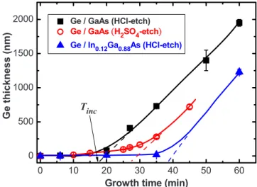
Effects of wet etching of Ga(In)As surfaces on incubation time of Ge growth.— It has been reported9that a specific incubation time is required for Ge growth on GaAs. In our study, this incubation time 共Tinc兲 was still dependent on the type of etched Ga共In兲As surface.
Figure3displays the thickness variation in the grown Ge layers vs growth time共Tg兲 on a GaAs HCl surface, a GaAs H2SO4surface, and a GaInAs HCl surface. For all these surfaces, the Ge growth rate was zero at the beginning, and later, the Ge grew at a very low growth rate. After a critical time, the Ge entered into a steady growth共corresponding to the linear region of plots for Ge thickness vs growth time in Fig.3兲. If the incubation time 共Tinc兲 is defined as the intersection between the line corresponding to the steady growth and the growth time axis, then from Fig.3, Ge growth requires a longer Tinc 共⬃28 min兲 on a GaAs H2SO4surface than on a GaAs HCl surface 共Tinc⬃ 19 min兲, and Ge growth on a Ga0.88In0.12As HCl surface requires the longest Tinc 共⬃37 min兲. Bai et al.9 re-ported that the Ge growth on GaAs was initiated via the formation of a Ge–Ga bond because the Ge–Ga bond has a lower formation energy than the Ge–As bond. A rich arsenic 共As兲 coverage on a GaAs surface could block Ge atoms from bonding with Ga atoms and thus impede Ge adatom attachment, leading to the long incuba-tion time. In other words, a GaAs surface with a higher Ga-to-As ratio facilitates Ge nucleation and epitaxy because there are more available Ga sites for Ge adatoms to bond. Next, we demonstrate, by using XPS, that the Tincis truly related to the amount of As on the GaAs. Figure4apresents the As 3d photoemission spectra for the GaAs HCl surface and the GaAs H2SO4surface. The deconvoluted peaks of the As–As, AsOx, As2O3, and As2O5species appeared in the spectra at binding energies of 0.9, 2, 3.4, and 4.4 eV, respec-tively, above that of the GaAs substrate. Obviously, the amounts of both As–As and As oxides were higher for the GaAs substrate re-ceiving a H2SO4rinse. In this work, the deconvolution process was also performed on the spectra of Ga 3d core level, and we thus evaluated the signal ratios of all chemical species on the etched GaAs substrates, as summarized in Fig.4b. The GaAs HCl surface has an As coverage of 11.8%, and the GaAs H2SO4surface has an As coverage of 21.4%. Correspondingly, the growth of Ge on these two surfaces has an incubation time of 19 and 28 min, respectively, indicating that more As coverages on the GaAs surface lead to a longer incubation time for Ge growth. Regarding the growth of Ge on a GaInAs surface, it is speculated that the In–Ge bond, like the As–Ge bond, also has a higher formation energy than the Ga–Ge
0.2μμm GaAs Ga1-xInxAs graded buffer Ga0.88In0.12As 0.2μμm 0.2μμm GaAs Ga1-xInxAs graded buffer Ga0.88In0.12As
Figure 1. The XTEM image of Ga0.88In0.12As virtual substrates. Most
dislo-cations are confined inside the Ga1−xInxAs-graded buffer layer, and the top 0.3 m Ga0.88In0.12As has a much reduced threading dislocation density.
0 100 200 300 400 500 600 700 800 0 200 400 600 800 1000 H3PO4(aq.) H3PO4(aq.) H2SO4(aq.) H2SO4:H2O2:H2O = 1:8:1000 Rate ~0.53 nm/s H2SO4:H2O2:H2O = 6:2:150 Rate ~1.4 nm/s H3PO4:H2O2:H2O = 6:1:150 Rate ~0.3 nm/s H3PO4:H2O2:H2O = 6:2:150 Rate ~0.785 nm/s E tch in g d ep th ∆∆ H( n m )
Etching time (sec)
H2SO4(aq.)
∆∆H GaAs
SiO2
Figure 2.共Color online兲 GaAs etching depth vs etching time for the different chemical solutions. The inset shows the actual process through which the etching thickness can be easily measured. These data can supply a reference for the recess formation on the GaAs substrate.
0 10 20 30 40 50 60 0 500 1000 1500 2000 Ge / GaAs (HCl-etch) Ge / GaAs(H2SO4-etch) Ge / In0.12Ga0.88As (HCl-etch) G e thi ckness (nm )
Growth time (min)
Tinc
Figure 3.共Color online兲 Ge growth thickness vs growth time on the different Ga共In兲As surfaces. The solid lines are drawn as a guide for the eyes. The incubation times共Tin兲 for Ge grown on GaAs HCl surface, on GaAs H2SO4 surface, and on GaInAs HCl surface are 19, 28, and 37 min, respectively. H28 Journal of The Electrochemical Society, 157共1兲 H27-H30 共2010兲
H28
) unless CC License in place (see abstract).
ecsdl.org/site/terms_use
address. Redistribution subject to ECS terms of use (see
140.113.38.11
bond; thus, In, like As, also tends to impede Ge adatom attachment, so the available Ga sites on the GaInAs surface for Ge adatoms to bond are obviously less than those on GaAs surfaces, resulting in the longest observed incubation time for the growth of Ge on GaInAs.
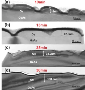
Ge growth behavior on GaAs.— Figure5shows XTEM images of the Ge layer at the initial growth stage. The GaAs substrate here was etched by the chemical solution of H2SO4:H2O2:H2O = 6:2:150 before Ge UHV/CVD growth.
At the first stages, the Ge film grew in island mode. With the continuance of growth, the islands started to merge and then formed a blanket film. When the growth time was long enough, the surface of the Ge layer became flat. Figure5also reveals that, before form-ing a blanket film, the Ge islands grew tall at almost the same height and merged with two-dimensional spreading. For the lattice-mismatch material system, such as Ge/Si and GaInAs/GaAs, the initial growth mode of film also start as islands, and island formation is driven by the lattice-mismatch-induced strain.10However, for Ge on GaAs, there is no lattice-mismatch strain between Ge and GaAs, and so the mechanism of Ge island formation on GaAs must be different from that of Ge/Si or GaInAs/GaAs. Through detailed studies of the surface morphology of Ge films on GaAs共100兲 by using low energy electron diffraction and scanning tunneling mi-croscopy, Wang et al.5reported that the Ge islands on GaAs共100兲 are in Stranski–Krastanov mode; the driving force for the formation of this mode is a reduction in the total surface energy by minimizing substrate-induced electronic effects.
Figure6shows the TEM image of Ge共Tg= 35 min兲 selectively grown in the recessed GaAs regions. A good quality Ge epitaxy without dislocation formation was achieved. No Ge was deposited
onto the SiO2region, which indicates a better selective growth of Ge on GaAs than on SiO2. As mentioned in the introduction section, the III-V materials are being considered as high mobility channels for further high speed and low power metal-oxisemiconductor de-vice applications. However, so far, the drive current of the III-V MOSFET has not outperformed Si at the sub-100 nm channel length. The root cause is related not only to the dielectric–substrate interface quality but also to the lower density of states and the lim-ited dopant level for III-V.11 We thus propose that the structure shown in Fig. 6 could potentially tackle these critical issues and hence boost the current drive capability by using Ge as the hetero-structural source–drain of a GaAs nMOSFET.
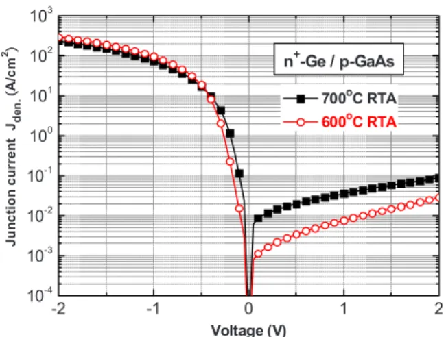
The fabricated n⫹-Ge/p-GaAs diode.— Figure 7 shows the di-ode characteristics of the n+-Ge/p-GaAs heterojunctions undertak-ing dopant activation at 600 and 700°C. Compared to the properties of the 700°C annealed diode, the 600°C annealed sample actually
46 45 44 43 42 41 40 39
Binding energy (eV)
Photoel e c tr on in te nsi ty (arb. u n it s ) As2O5 As2O3 AsOx As-As H2SO4+DIW+HCl+DIW HCl+DIW only GaAs sub. (a) As3d 0 20 40 60 80 100 19.7 8.2 11.8 60.3 GaAs As-As As2Ox Ga2Ox C o mpos itions in G a A s3d co re level (%)
Wet-chemical clean conditions HCl+DIW only H2SO4+DIW+HCl+DIW
21.4
13.4 13.8 51.4
(b)
Figure 4. 共Color online兲 共a兲 The As 3d XPS spectra of the GaAs surfaces subjected to different acid etchants and共b兲 the analysis of composition ratio on the etched GaAs surfaces revealed by XPS.
Figure 5. 共Color online兲 The XTEM images of Ge layer on GaAs substrate at different growth times:共a兲 10, 共b兲 15, 共c兲 25, 共d兲 30, and 共e兲 50 min.
GaAs Ge Ge GaAs p-GaAs sub. Ge drain Ge source Dummy-SiO2 295 nm GaAs Ge Ge GaAs p-GaAs sub. Ge drain Ge source Dummy-SiO2 295 nm
Figure 6.共Color online兲 The XTEM images of Ge layer selectively grown into the recessed region of GaAs substrate. The Ge layer has an excellent SEG on GaAs compared with that on SiO2.
H29
Journal of The Electrochemical Society, 157共1兲 H27-H30 共2010兲 H29
) unless CC License in place (see abstract).
ecsdl.org/site/terms_use
address. Redistribution subject to ECS terms of use (see
140.113.38.11
exhibited a higher forward current共JF兲 along with a lower reverse leakage current共JR兲. The magnitude of the rectifying ratio can be up to 4 orders共in the voltage range of ⫾1 V兲, where the values of JF and JR were 9.5⫻ 101and 7.7⫻ 10−3 A/cm2, respectively. Rais-ing the temperature to 700°C resulted not only in a slight degrada-tion of the JFto 7.2⫻ 101 A/cm2but also in an increase in the JR to 3.6⫻ 10−2 A/cm2. From the J
Rcharacteristics of both 600 and 700°C annealed samples, we also noticed that the JR–VR 共reverse voltage兲 curves slightly deviate from that predicted by the Shockley–Read–Hall theory, where JR has a square root of VR de-pendence, implying the possible onset of the trap-assisted tunneling mechanism in these diodes. Moreover, for the 600°C annealed di-ode, the ideality factor nf of 1.17 and the series resistance Rs of 41.4 ⍀ were extracted from their JFcharacteristics, with values of 1.42 and 48.5 ⍀ for the nf and Rs of the 700°C activated diode, respectively. The corresponding barrier height⌽bwas estimated to be 0.52共⫾0.04兲 eV for the 600°C diode, and it decreased slightly to 0.48共⫾0.04兲 eV for the 700°C diode, where the variation comes from the uncertainty in the Richardson constant Aⴱ. In terms of the
above experimental results, the diode characteristics of these n+-Ge/p-GaAs heterojunctions are acceptable, but still, more opti-mization work is needed.
Conclusions
Ge epitaxial growth on GaAs共100兲 substrates and
Ga0.88In0.12As共100兲 virtual substrates was studied by using a UHV/ CVD system. The incubation time of Ge growth depended on the different Ga共In兲As surfaces going through different wet chemical processes. One explanation considered the dependence on the num-ber of available Ga sites for the bonding of Ge adatoms on different Ga共In兲As surfaces. Fewer Ga sites tended to prolong the incubation time. In this study, Ge was easily grown selectively into GaAs re-cessed regions with good quality. Based on the grown material, an n+-Ge/p-GaAs diode was fabricated. The diode showed a normal rectifying characteristic, with the rectifying ratio being up to 4 or-ders of magnitude. These experimental results imply that Ge growth on GaAs can provide an additional way to integrate Ge and GaAs. For example, Ge can possibly be used as the hetero-source/drain of GaAs nMOSFET to further enhance the device performance.
National Nano Device Laboratories assisted in meeting the publication costs of this article.
References
1. S. E. Thompson, M. Armstrong, C. Auth, S. Cea, R. Chau, G. Glass, T. Hoffman, J. Klaus, M. Zhiyong, B. Mcintyre, et al., IEEE Electron Device Lett., 25, 191 共2004兲.
2. K. Rim, S. Koester, M. Hargrove, J. Chu, P. M. Mooney, J. Ott, T. Kanarsky, P. Ronsheim, M. Leong, A. Grill, and H.-S. P. Wong, Dig. Tech. Pap. - Symp. VLSI Technol., 2001, 59.
3. Y. Sun, E. W. Kiewra, J. P. De Souza, J. J. Bucchignano, K. E. Fogel, D. K. Sadana, and G. G. Shahidi, IEEE Electron Device Lett., 30, 5共2009兲, and references therein.
4. G. L. Luo, Y. C. Hsieh, E. Y. Chang, M. H. Pilkuhn, C. H. Chien, T. H. Yang, C. C. Cheng, and C. Y. Chang, J. Appl. Phys., 101, 084501共2007兲.
5. X. S. Wang, K. W. Self, and W. H. Weinberg, J. Vac. Sci. Technol. A, 12, 1920 共1994兲.
6. J. Falta, M. C. Reuter, and R. M. Tromp, Appl. Phys. Lett., 65, 1680共1994兲. 7. C. B. Ebert, L. A. Eyres, M. M. Fejer, and J. S. Harris, J. Cryst. Growth, 201–202,
187共1999兲.
8. M. Zhu, H. C. Chin, G. S. Samudra, and Y. C. Yeo, J. Electrochem. Soc., 155, H76 共2008兲.
9. Y. Bai, K. E. Lee, C. W. Cheng, M. L. Lee, and E. A. Fitzgerald, J. Appl. Phys.,
104, 084518共2008兲.
10. K. Brunner, Rep. Prog. Phys., 65, 27共2002兲.
11. M. V. Fischetti, L. Wangt, B. Yu, C. Sachs, P. M. Asbeck, Y. Taur, and M. Rodwell, Tech. Dig. - Int. Electron Devices Meet., 2007, 109.
-2 -1 0 1 2 10-4 10-3 10-2 10-1 100 101 102 103 Ju n c ti o n c u rr e n t Jde n. (( A/ c m 2)) Voltage (V) 700oC RTA 600oC RTA n+-Ge / p-GaAs
Figure 7.共Color online兲 The diode characteristics of n+-Ge/p-GaAs
hetero-junction with dopant activation at 600 and 700°C for 30 s, respectively.
H30 Journal of The Electrochemical Society, 157共1兲 H27-H30 共2010兲
H30
) unless CC License in place (see abstract).
ecsdl.org/site/terms_use
address. Redistribution subject to ECS terms of use (see
140.113.38.11